Case Study
Clock Distribution Networks for Three-Dimensional ICs
Abstract
A prototype circuit, the second of the three prototype circuits presented in this book, investigating different global three-dimensional (3-D) clock distribution networks, is described in this chapter. A variety of clock networks such as H-trees, rings, tree-like networks, and trunk-based networks, are explored in terms of clock skew and power consumption to determine an effective clock distribution network for 3-D ICs. The prototype test circuit composed of these networks is manufactured by the 3-D fabrication process developed at MIT Lincoln Laboratories. The design and modeling process and related experimental results are also included in this chapter. Power and clock skew tradeoffs among the different topologies are presented.
Keywords
3-D global clock distribution networks; 3-D H-trees; clock skew modeling
As discussed in the previous chapter, an omnipresent and challenging issue for synchronous digital circuits is the reliable distribution of the clock signal to the many thousands to millions of sequential elements distributed throughout a synchronous circuit [574]. The complexity is further increased in three-dimensional (3-D) ICs as sequential elements belonging to the same clock domain (i.e., synchronized by the same clock signal) can be located on different tiers.
In this chapter, a variety of clock network architectures for 3-D circuits is discussed. These clock topologies have been included on a test circuit for the 3-D technology developed at MIT Lincoln Laboratories (MITLL). This fabrication process is discussed in the following section. The logic circuitry comprising the common load of the 3-D clock distribution networks is described in Section 16.2. The several clock distribution networks employed in this case study are described in Section 16.3. Models used to simulate these clock distribution networks are discussed in Section 16.4. Experimental results and a comparison of the different clock distribution networks are presented in Section 16.5. A short summary is provided in the last section of the chapter.
16.1 MIT Lincoln Laboratories Three-Dimensional IC Fabrication Technology
The MITLL developed a manufacturing process for fully depleted silicon-on-insulator (FDSOI) 3-D circuits with short intertier vias (also called 3-D vias here for simplicity). The usual term through silicon via (TSV) is rather misleading for this process as the silicon substrate is fully removed and only the silicon oxide remains. The most attractive feature of this process is the high density of the 3-D vias as compared to other 3-D technologies currently under development, as reviewed in Chapter 3, Manufacturing Technologies for Three-Dimensional Integrated Circuits. The MITLL process is a wafer level 3-D integration technology with up to three FDSOI wafers bonded to form a 3-D circuit. The diameter of the wafers is 150 mm. The minimum feature size of the devices is 180 nm, with one polysilicon layer and three metal layers interconnecting the devices on each wafer. A backside metal layer also exists on the upper two tiers, providing the starting and landing pads for the 3-D vias, and the I/O, power supply, and ground pads for the entire 3-D circuit. The primary steps of this fabrication process are illustrated in Figs. 16.1 through 16.6 [177,307].


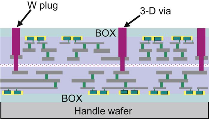

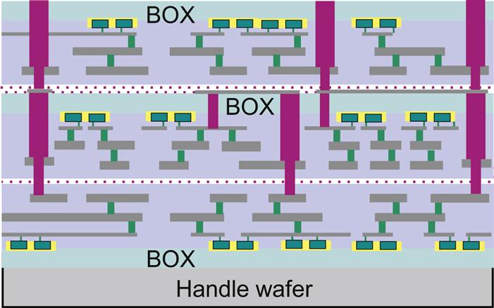

Each of the wafers is manufactured by a mainstream FDSOI process (Fig. 16.1). The second wafer is flipped and face-to-face bonded with the first wafer using oxide bonding (Fig. 16.2). The handle wafer is removed from the second wafer and the 3-D vias are etched through the oxide of both tiers. Tungsten is deposited to fill the 3-D vias, and the surface of the wafer is planarized by chemical mechanical polishing (Fig. 16.3). The backside vias and metallization are formed to provide the pads for the 3-D vias of the third wafer and the interconnection of these vias with the M1 layer of the second wafer (Fig. 16.4). The third wafer is also flipped and face-to-back bonded with the second tier (Fig. 16.5). Another etching step is used to form the 3-D vias of the third tier. The backside vias and interconnections are formed along with the I/O and power pads for the 3-D circuit. A deposited glass coating provides the passivation layer, while the overglass cuts create the necessary pad openings for the off-chip interconnections (Fig. 16.6).
A salient characteristic of this process is the short 3-D vias. As illustrated in Fig. 16.7, the total length of a 3-D via that connects two devices on the first and third tier is approximately 20 μm. In addition, the dimensions of these vias are 1.75 μm×1.75 μm, much smaller than the size of the TSV in many existing 3-D technologies, as discussed in Chapter 3, Manufacturing Technologies for Three-Dimensional Integrated Circuits. The spacing among the 3-D vias depends upon the density of these vias and ranges from 1.75 μm to 8 μm. Note that the 3-D vias connecting the second and third tier can be vertically stacked, resulting in 3-D vias that directly connect devices on the first and third tiers.
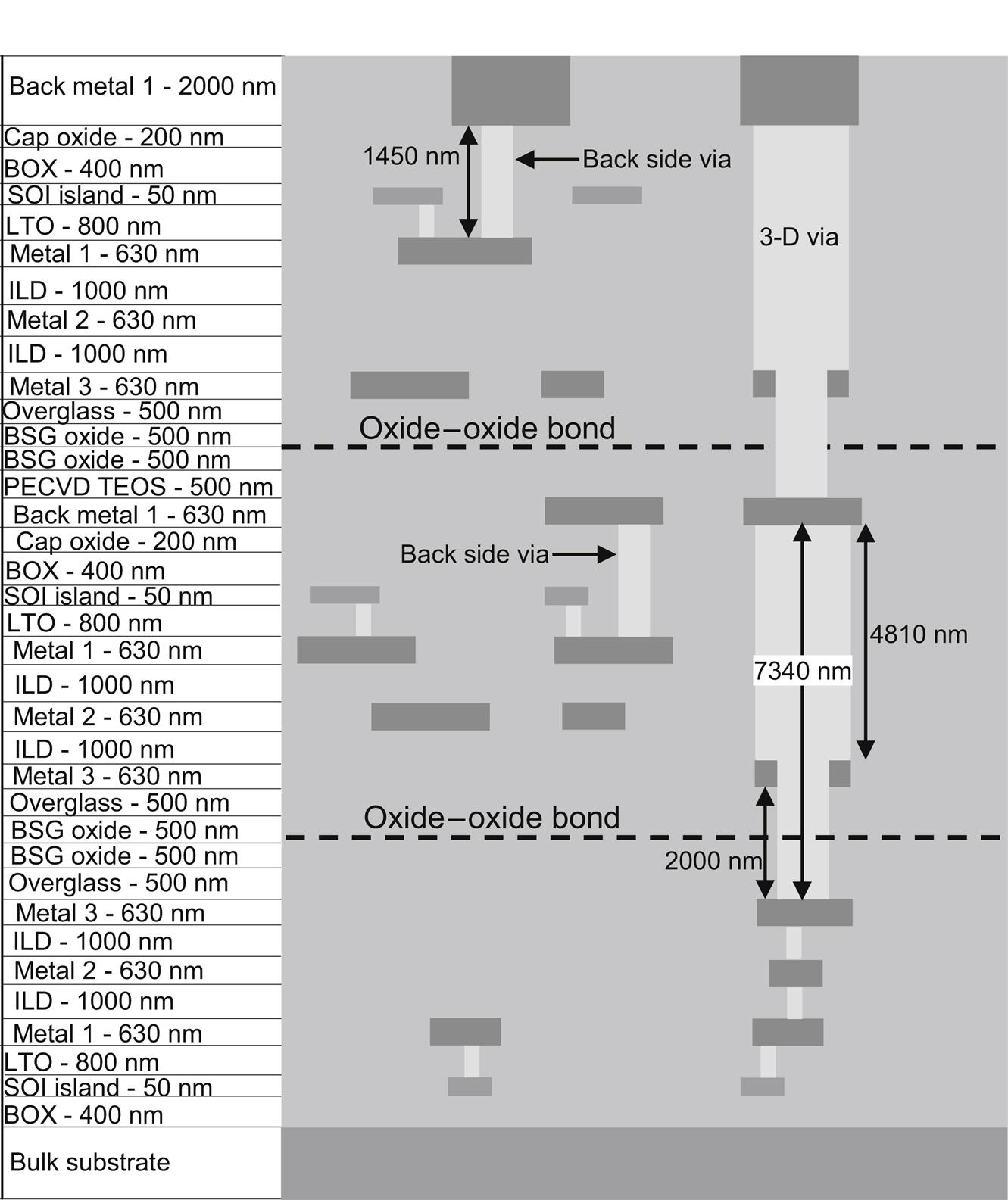
A doughnut shaped structure is required for the 3-D vias in both the second and third tier to provide mechanical support for these vias. As shown in Fig. 16.7, the 3-D vias connect different metal layers in the second and third tier. A 3-D via for the second tier connects the backside metal with the M3 layer of the first tier through the doughnut formed by M3 in the second tier. The backside vias or the M3 layer of the second tier connects the 3-D via with the devices on that tier. Alternatively, a 3-D via for the third tier starts from the backside metal of the third tier and ends on the backside metal of the second tier through a doughnut formed by the M3 layer of the third tier. The backside vias connect this via with the devices on the second tier. The transistors located on the third tier are connected to the 3-D via either through the backside metal layer and backside vias, or through the M3 doughnut that surrounds the 3-D via. Note that the 3-D vias can be placed anywhere within the circuit and not only within certain regions. The minimum distance from the transistors, however, is specified by the design rules and is less than 1.5 μm for the MITLL 3-D process.
The electrical sheet resistance of the metal and diffusion layers is listed in Table 16.1 along with the bulk resistivity. The total resistance of the intratier vias and contacts is listed in Table 16.2. Since the third tier is also intended for RF circuits, a low resistance backside metal is available. In addition to the active devices, passive elements, such as resistors and metal-insulator-metal (MIM) capacitors, are also available. The resistors, however, can only be placed on the third tier where the polysilicon or active layer is utilized to form these resistors.
Table 16.1
Layer Resistances of the 3-D FDSOI Process [307]
| Parameter | Value |
| Bulk resistivity | ~2,000 Ω-cm |
| Silicided n+/p+ active sheet resistance | 15±3 Ω/sq. |
| Silicided n+/p+ polysilicon sheet resistance | 15±3 Ω/sq. |
| Silicided n+/p+ sheet resistance | 15±3 Ω/sq. |
| Lower metal layer sheet resistance | ~0.12 Ω/sq. |
| Top metal layer sheet resistance | ~0.08 Ω/sq. |
| Backside metal sheet resistance | ~0.12 Ω/sq. |
Table 16.2
Contact and Via Resistances of the 3-D FDSOI Process [307]
| Parameter | Value |
| Poly contact (250 nm×250 nm) | 10±2 Ω |
| n+ active contact (250 nm×250 nm) | 10±2 Ω |
| p+ active contact (250 nm×250 nm) | 10±2 Ω |
| Interconnect metal via (300 nm×300 nm) | 4 Ω |
| Backside metal via (500 nm×500 nm) | 2 Ω |
In support of this manufacturing process, design kits for this technology have been developed by academic institutions and supporting CAD companies. The process design kit has been developed for the Cadence Design Framework by faculty from North Carolina State University [421]. This kit includes device models for circuit simulation and a sophisticated layout tool for 3-D circuits. For example, circuits located on a specific tier can be separately visualized or highlighted. In addition, a circuit designed for one tier can be reproduced or transferred to another tier. Complete design rule checking and circuit extraction are also available. Electrical rule checking, however, is not included, meaning that these 3-D circuits cannot be directly checked for shorts between the power and ground lines. However, to mitigate this problem, two pins can be assigned different names on the power and ground lines. Design rule checking reports errors whenever nets with different names are crossed, thereby checking for electrical shorts.
16.2 Three-Dimensional Test Circuit Architecture
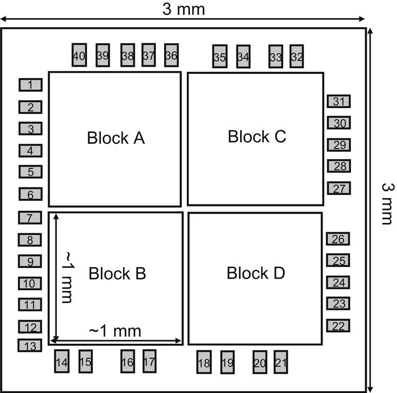
A test circuit exploring a variety of clock network topologies suitable for 3-D ICs has been designed based on the process described in the previous section. A block diagram of the test circuit is depicted in Fig. 16.8. The test circuit consists of four blocks. Each block contains the same logic circuit but implements a different clock distribution network. The total area of the test circuit is 3 mm×3 mm. The logic circuit common to all of these blocks is described in this section, while the different clock network topologies are discussed in Section 16.3.
An overview of the logic circuitry is depicted in Fig. 16.9. The function of this logic is to emulate different switching patterns characterizing the circuit and load conditions for the clock distribution networks under investigation. The logic is repeated in each tier and includes

The pseudorandom generators are based on the technique described in [613], which uses linear feedback shift registers and XOR operations to generate a random 16-bit word every clock cycle after the first few cycles required to initialize the generator. The physical layout of one random number generator is illustrated in Fig. 16.10. There are a total of nine pseudorandom generators in each circuit block, connected by groups of three to the crossbar switch within each tier.

A classic crossbar switch with six input and output ports is included in each tier, where the width of each port is 16 bits. Three of the six inputs of the crossbar switch are connected to the output of the number generators, while the remaining inputs are connected to ground. The physical layout of the crossbar switch is shown in Fig. 16.11. The three output ports of the switch are connected to a group of 4-bit counters, while the remaining outputs drive a small capacitive load. Since each port is 16 bits wide, each port is connected to four 4-bit counters. These counters are, in turn, connected to current loads implemented with cascoded current mirrors. The counters and current loads are distributed across each tier. The control logic consists of an 8-bit counter that controls the connectivity among the input and output ports of the crossbar switch.

The data flow in this circuit can be described as follows. After resetting the circuit, the pseudorandom number generators are initialized, and the control logic connects each input port to the appropriate output port. Since the control logic includes an 8-bit counter, each input port of the crossbar switch is successively connected every 256 clock cycles to each output port.
The output ports of the crossbar switch are connected to the 4-bit counters. Each of these counters is loaded with a 4-bit word, counts upwards, and loaded with a new word every time all of the bits are equal to one. The most significant bit (MSB) of each counter is connected to four current loads that are turned on when the bit is equal to one. Since the counters are loaded with random words from the random generators through the crossbar switch, the current loads draw a variable amount of current during circuit operation. This randomness mimics different switching patterns that can exist within a circuit.
The current loads are cascoded current mirrors, as shown in Fig. 16.12. In the cascoded current mirrors, the output current Iout closely follows Iref as compared to a simple current mirror. The reference current Iref is externally provided to control the amount of current drawn from the circuit. The gate of transistor M5 is connected to the MSB of a 4-bit counter, shown in Fig. 16.12 as the sel signal. This additional device switches the current sinks. The layout of a group of four current loads is illustrated in Fig. 16.13. The width of the devices shown in Fig. 16.12 is
(16.1)


The power supply is 1.5 volts, as set by the MITLL process.
The layout of the test circuit is illustrated in Fig. 16.14, while the connectivity of the pads to the external signals is listed in Table 16.3. Several decoupling capacitors are included in each circuit block and are highlighted in Fig. 16.14. The capacitors serve as extrinsic decoupling capacitance and are MIM capacitors. Note that the number of pads is not limited by the area of the circuit but, rather, by the maximum number of connections permitted by the probe card. The backside metal layer of the third tier is utilized for the pads. Each of the circuit blocks is supplied by separate power and ground pads, while only a pair of power and ground pads is connected to the pad ring to provide protection from electrostatic discharge.
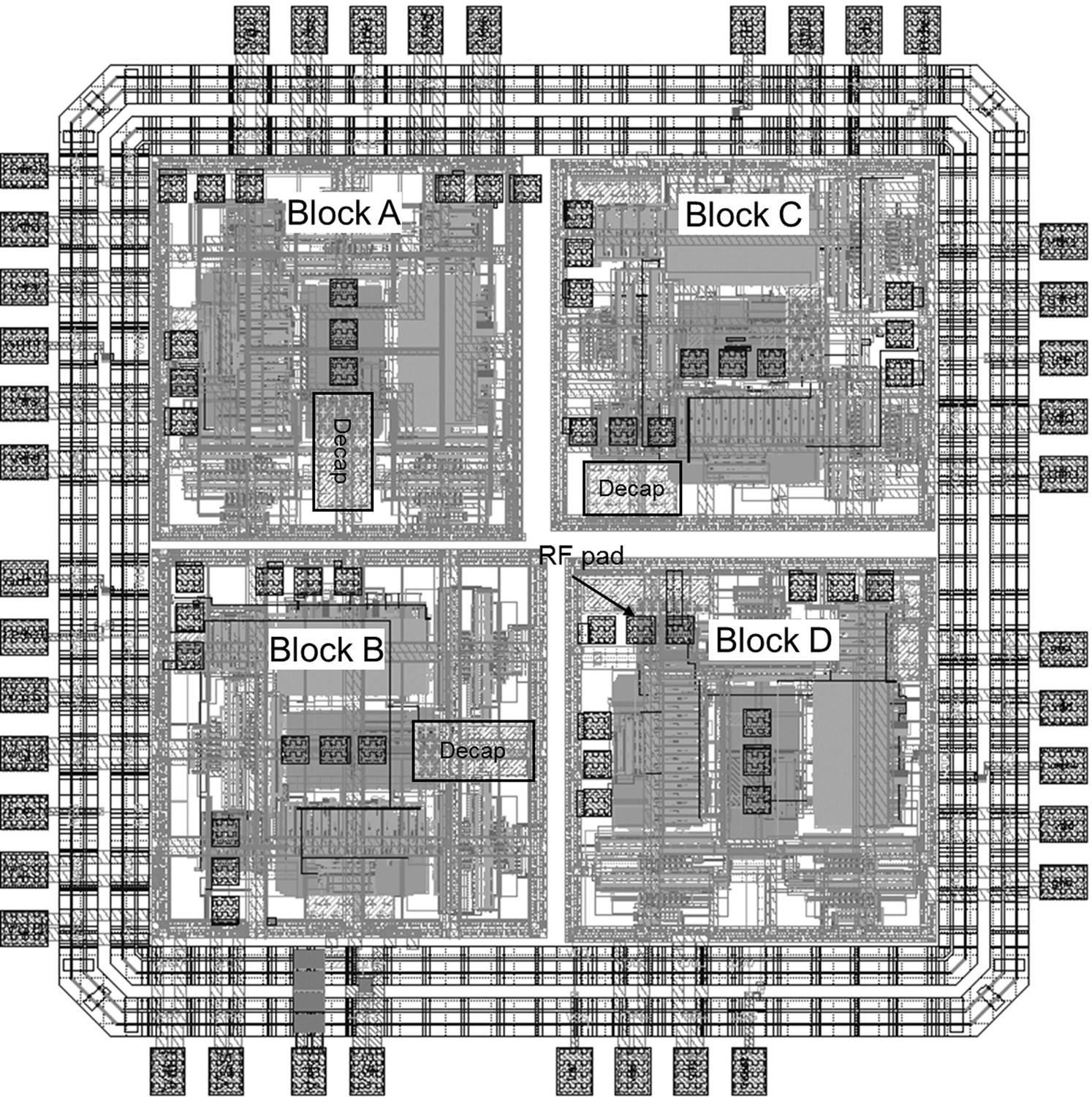
Table 16.3
Pad Connectivity of the 3-D Test Circuit (Pad Index Shown in Fig. 16.8)
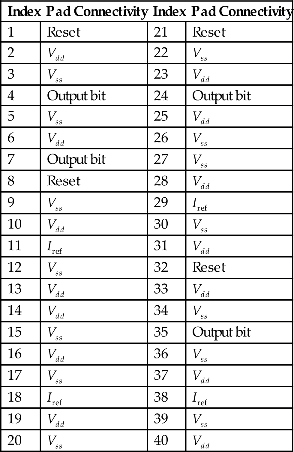
| Index | Pad Connectivity | Index | Pad Connectivity |
| 1 | Reset | 21 | Reset |
| 2 | Vdd | 22 | Vss |
| 3 | Vss | 23 | Vdd |
| 4 | Output bit | 24 | Output bit |
| 5 | Vss | 25 | Vdd |
| 6 | Vdd | 26 | Vss |
| 7 | Output bit | 27 | Vss |
| 8 | Reset | 28 | Vdd |
| 9 | Vss | 29 | Iref |
| 10 | Vdd | 30 | Vss |
| 11 | Iref | 31 | Vdd |
| 12 | Vss | 32 | Reset |
| 13 | Vdd | 33 | Vdd |
| 14 | Vdd | 34 | Vss |
| 15 | Vss | 35 | Output bit |
| 16 | Vdd | 36 | Vss |
| 17 | Vss | 37 | Vdd |
| 18 | Iref | 38 | Iref |
| 19 | Vdd | 39 | Vss |
| 20 | Vss | 40 | Vdd |
16.3 Clock Distribution Network Structures Within the Test Circuit
Different clock distribution schemes for 3-D circuits are described in this subsection. To evaluate the specific requirements of the clock networks, consider a traditional H-tree topology. As shown in Fig. 15.7, at each branch point of an H-tree, two branches emanate with the same length. An extension of the H-tree to three dimensions does not guarantee equidistant interconnect paths from the source to the leaves of the tree. This situation is shown in Fig. 16.15, where an H-tree is replicated in each tier of a 3-D circuit. The clock signal is propagated through intertier vias from the output of the clock driver to the center of the H-tree on tiers one and three. The high impedance of these vias increases the time for the clock signal to arrive at the leaves of the tree on these tiers as compared to the time for the clock signal to arrive at the leaves of the tree on the same tier as the clock driver. Furthermore, in a multi-tier 3-D circuit, three or four branches can emanate from each branch point. The third branch propagates the clock signal to the other tiers of the 3-D circuit, as shown in Fig. 16.15. Similar to a design methodology for a two-dimensional (2-D) H-tree topology, the width of each branch is reduced to a third (or more) of the segment preceding the branch point to match the impedance at the branch point. This requirement, however, is difficult to achieve as the third and fourth branches are connected by an intertier via. The vertical interconnects are of significantly different length as compared to the horizontal branches and also exhibit different impedance characteristics.

Several clock network topologies for 3-D ICs are investigated in this case study. Each of the four blocks of the test circuit includes a different clock distribution structure, which are schematically illustrated in Fig. 16.16. The physical layout of these topologies for the MITLL 3-D technology is depicted in Fig. 16.17. The architectures employed in the blocks are:
Block A: All of the tiers contain a four level H-tree (i.e., equivalent to 16 leaves) with identical interconnect characteristics. The H-trees are connected through a group of intertier vias at the first branching point, as shown in Fig. 16.16A. The second tier is face-to-face bonded with the first tier and both of the H-trees are placed on the third metal (M3) layer. The physical distance between these clock networks is approximately 2 μm. Note that the H-tree on the second tier is rotated by 90° with respect to the H-trees on the other two tiers. The orthogonal placement of these two clock networks effectively eliminates any inductive coupling. All of the H-trees are shielded with two parallel lines connected to ground.
Block B: A four level H-tree is included in the second tier. Each of the leaves of this H-tree is connected through intertier vias to small local rings on the first and third tier, as illustrated in Fig. 16.16B. As in Block A, the H-tree is shielded with two parallel lines connected to ground. Additional interconnect resources are used to form local meshes. Due to the limited interconnect resources, however, a uniform mesh in each ring is difficult to achieve. The clock routing is constrained by the power and ground lines as only three metal layers are available on each tier.
Block C: The clock distribution network for the second tier is a shielded four level H-tree. Two global rings are utilized for the other two tiers, as depicted in Fig. 16.16C. Each ring is connected through intertier vias to the four branch points on the second level of the H-tree. The registers in each tier are individually connected to the ring.
Block D: The clock network on each tier consists of a trunk structure and branches that connect the registers in each tier to the trunk, as shown in Fig. 16.16D. As for Block A, the trunk for the second tier is rotated by 90° to avoid inductive coupling. Those interconnects that branch from the trunk are placed as close as possible to the registers.


Buffers are inserted at appropriate branch points within the H-trees to amplify the clock signal. In each of the circuit blocks, the clock driver for the entire clock network is located on the second tier. The clock driver on that tier is placed to ensure that the clock signal propagates through similar vertical interconnect paths to the first and third tier, resulting in the same approximate delay for the registers located on the first and third tiers. The clock driver is a traditional chain of tapered buffers [614–617].
The clock network on each tier feeds the registers located on the same tier. The off-chip clock signal is passed to the clock driver through an RF pad, as shown in Fig. 16.18. The dimensions of the RF pad are also shown in Fig. 16.18. Additional RF pads are placed at different locations on the third tier of each block for probing. These RF pads are used to measure the clock skew at different locations on different tiers within the clock network. The output circuitry is an open drain transistor connected to the RF pads by a group of intertier vias to decrease the resistance between the transistor and the probe. The probe is modeled as a series RLC impedance with the values shown in Fig. 16.19. The circuit depicted in Fig. 16.19 is used to determine the size of the output transistor.


In addition to the clock skew within the clock network topologies employed within the blocks of the test circuit, the power consumption of the entire clock distribution network has also been measured. Since all of the blocks include the same logic circuits, any difference in power consumption is attributed to the clock network, including the interconnect structures, clock driver, and clock buffers. The simulations characterizing the clock delay for each topology are described in the following section. The measurements of the clock skew and power dissipation of the blocks are discussed in the following Section 16.5.
16.4 Models of the Clock Distribution Network Topologies Incorporating Three-Dimensional Via Impedance
Simulation of the fabricated clock distribution topologies incorporating the electrical impedance of the intertier 3-D vias is described in this section. A comparison between the simulated and experimental results is also presented here. The electrical impedance of the 3-D vias is evaluated for several diameters, lengths, dielectric thicknesses (bulk), and via-to-via spacings [58,201]. These expressions are used here to model the contribution of the 3-D vias to the delay and skew characteristics of the clock distribution topologies, and are described in detail in Chapter 4, Electrical Properties of Through Silicon Vias.
In addition to characterizing the electrical parameters of the TSVs, the electrical characteristics of the clock distribution network on each tier are determined through numerical simulation. This set of simulations has been performed for the three widths used in the fabricated test circuit, and for five different lengths. Trend lines for the capacitance, DC resistance, 1 GHz resistance, DC self- and mutual inductance, and the asymptotic self- and mutual inductance fasym approximate the electrical parameters of different length interconnect segments within the clock network. These simulations include two ground return paths spaced 2 μm from either side of the clock line. These return paths behave as ground for the electrical field lines emanating from the clock line, resulting in a more accurate estimate of the capacitance.
The electrical paths of the clock signal propagating from the root to the leaves of each tier for the H-tree clock topology (see Fig. 16.16A) is depicted in Fig. 16.20. The clock network on each tier is modeled by 50 μm segments, where a π network represents the electrical properties of each segment. These 50 μm segments model the distributive electrical properties of the interconnect. Similarly, when either meshes (Fig. 16.16B) or rings (Fig. 16.16C) are used on tiers A and C (see Fig. 16.20), each 50 μm segment is replaced with an equivalent π network to more accurately represent the single mesh and ring structure within the test circuit. Note that for the mesh structures, the clock signal is distributed to tiers A and C from the leaves of the H-tree in tier B. For the rings topology, the clock signal distributed within tiers A and C is driven by buffers at the second level of the H-tree. The delay from the root to the leaves of each tier is listed in Table 16.4.
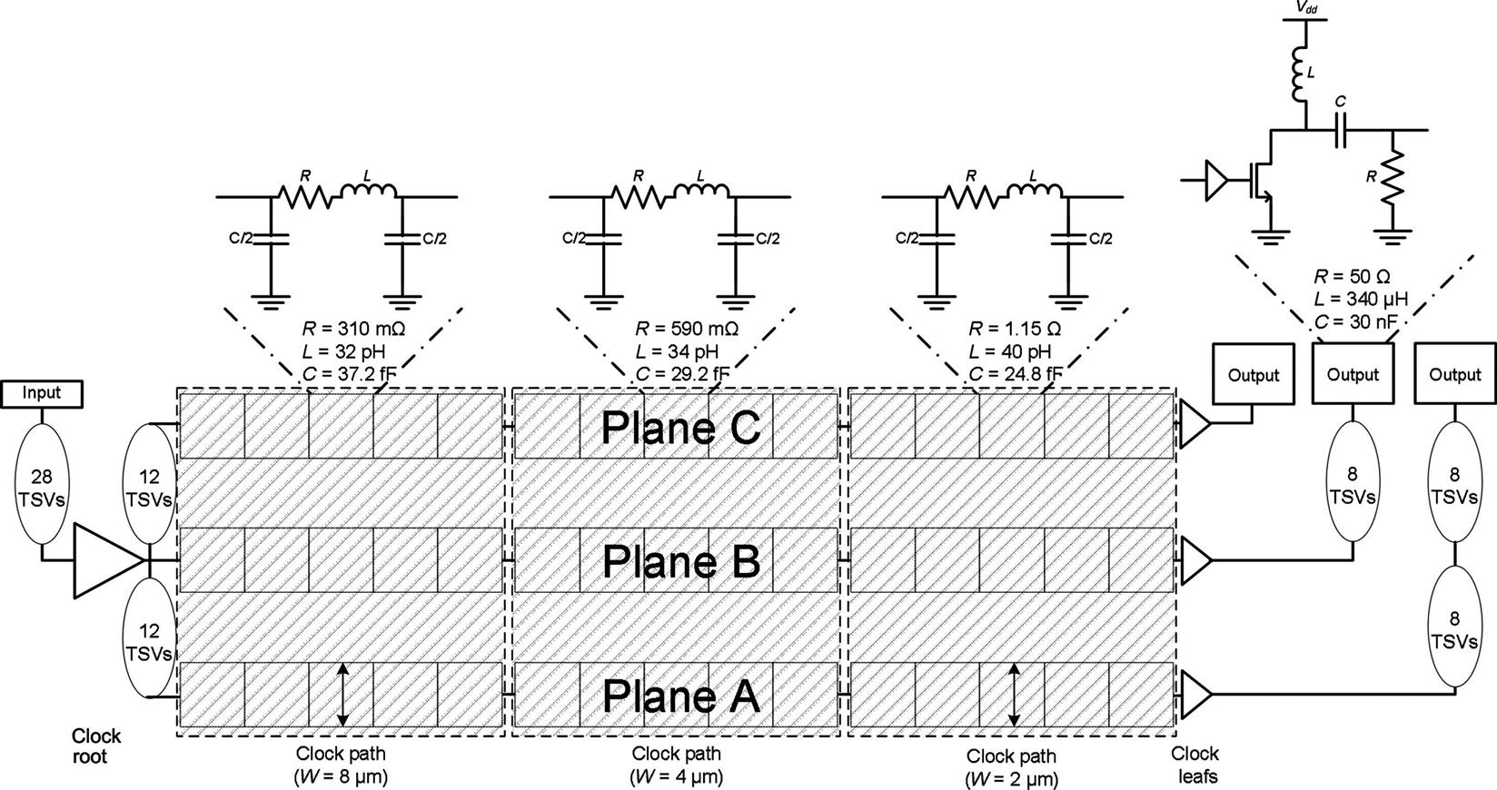
Table 16.4
Modeled Clock Delay From the Root to the Leaves of Each Tier for Each Block
| Clock Distribution Network | Clock Delay (ns) | ||
| tA | tB | tC | |
| H-trees (Fig. 16.16A) | 0.359 | 0.355 | 0.351 |
| Local rings (Fig. 16.16B) | 0.325 | 0.323 | 0.321 |
| Global rings (Fig. 16.16C) | 0.510 | 0.465 | 0.442 |
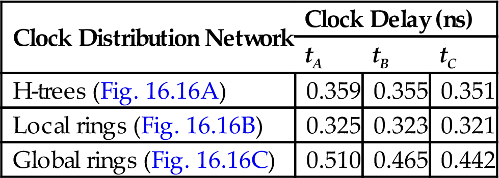
Good agreement between the model and experimental data is shown. The per cent error between the model and experimental clock delays is listed in Table 16.5. A maximum error of less than 10% is achieved for the clock paths within the H-tree topology. The larger errors listed in Table 16.5 are due to the small time scale being examined.
Table 16.5
Per cent Error Between Modeled and Experimental Clock Delay
| Clock Distribution Network | Clock Delay % Error | ||
| tA | tB | tC | |
| H-trees (Fig. 16.16A) | 0 | −4.8 | −7.4 |
| Local rings (Fig. 16.16B) | 36.9 | 8.4 | −6.5 |
| Global rings (Fig. 16.16C) | 3.9 | 3.2 | 0.7 |

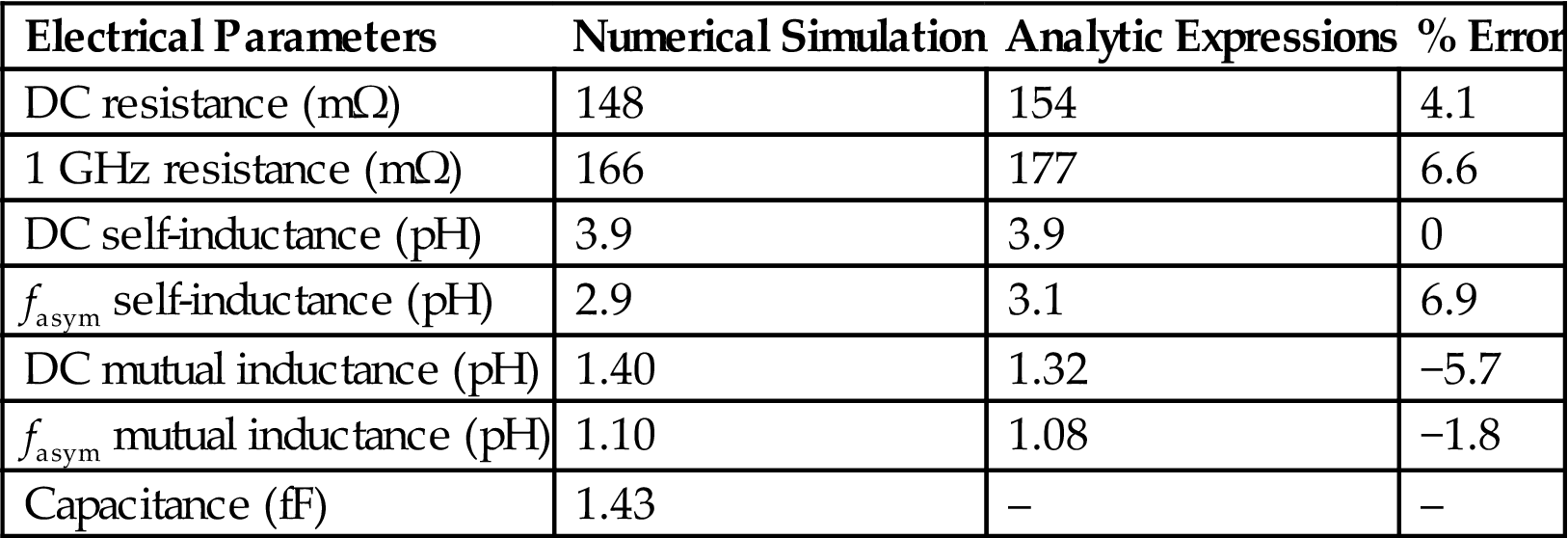
The equivalent electrical model of a TSV used for the simulation of the clock networks is shown in Fig. 16.21. The resistance, inductance, and capacitance expressions are compared to numerical simulations for the TSV structures in the MITLL multiproject wafer (for 3-D via parameters, r=1 μm, l=8.5 μm, and p=5 μm) in Table 16.6.

Table 16.6
Comparison of Numerical Simulations and Analytic Expressions of the TSV Electrical Parameters
| Electrical Parameters | Numerical Simulation | Analytic Expressions | % Error |
| DC resistance (mΩ) | 148 | 154 | 4.1 |
| 1 GHz resistance (mΩ) | 166 | 177 | 6.6 |
| DC self-inductance (pH) | 3.9 | 3.9 | 0 |
| fasym self-inductance (pH) | 2.9 | 3.1 | 6.9 |
| DC mutual inductance (pH) | 1.40 | 1.32 | −5.7 |
| fasym mutual inductance (pH) | 1.10 | 1.08 | −1.8 |
| Capacitance (fF) | 1.43 | – | – |
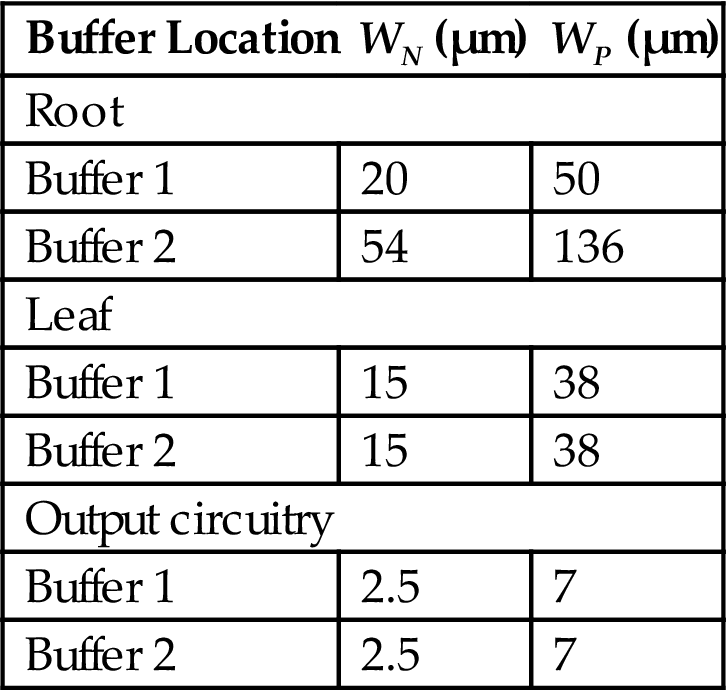
The circuit parameters used to model the delay within the clock network are provided below. The dimensions of the buffer circuits at the root, leaves, and output circuitry are listed in Table 16.7. Two sets of transistor widths are provided as each location is double buffered to maintain the same signal logic level. The dimensions of the ring and a single mesh are listed in Table 16.8. These lengths are partitioned into 50 μm long segments, and each segment is modeled by an equivalent π network for a line width of 4 μm. The source follower NMOS transistor located in the output circuitry has a length of 180 nm and a width of 12 μm. The interconnect length connecting the output circuitry and pads to the leaves on each of the three device tiers varies from 0 to 150 μm depending upon the clock topology (line width of 2 μm) and is also represented by an equivalent π network.
16.5 Experimental Results
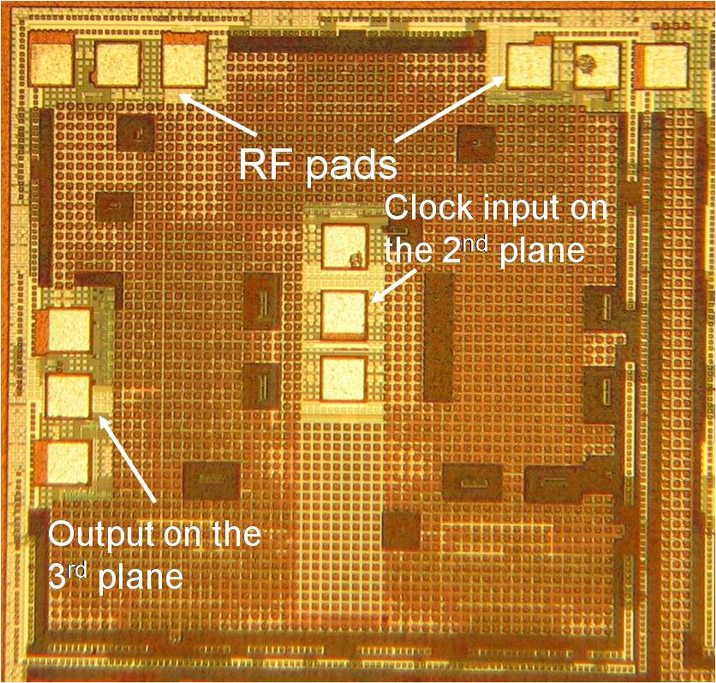
The clock distribution network topologies of the 3-D test circuit are evaluated in this section. The fabricated circuit is depicted in Fig. 16.22, where the four individual blocks can be distinguished. A magnified view of one block is shown in Fig. 16.23. Each block includes four RF pads for measuring the delay of the clock signal. The pad located at the center of each block receives the input clock signal. The clock input is a sinusoidal signal with a DC offset, which is converted to a square waveform at the output of the clock driver. The remaining three RF pads are used to measure the delay of the clock signal at specific points on the clock distribution network within each tier. A buffer is connected to each of these measurement points. The output of this buffer drives the gate of an open drain transistor connected to the RF pad. The RF probes landing on these pads are depicted in Fig. 16.24, where the die assembly on the probe station is illustrated.


A clock waveform acquired from the topology combining an H-tree and global rings, shown in Fig. 16.16C, is illustrated in Fig. 16.25, demonstrating operation of the circuit at 1.4 GHz. The clock skew between the tiers of each block is listed in Table 16.9. The topologies are ordered in Fig. 16.26 in terms of the maximum measured clock skew between two tiers. The delay of the clock signal from the RF input pad at the center of each block to the measurement point on tier i is denoted as ![]() in Table 16.9. For example,
in Table 16.9. For example, ![]() denotes the delay of the clock signal to the measurement point on tier A. Additionally, the skew, the difference in the delay of the clock signal between two measurement points on tiers i and j, is notated as
denotes the delay of the clock signal to the measurement point on tier A. Additionally, the skew, the difference in the delay of the clock signal between two measurement points on tiers i and j, is notated as ![]() .
.
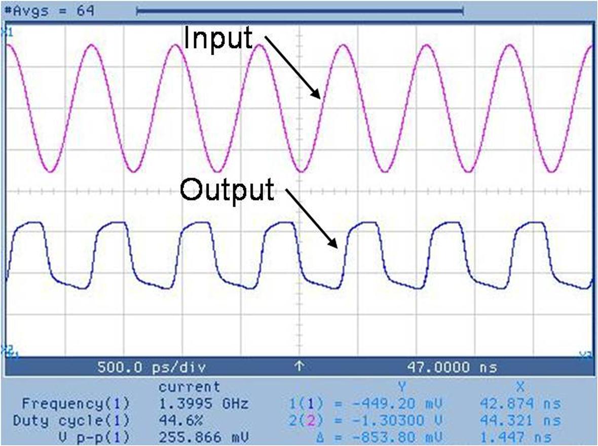
Table 16.9
Measured Clock Skew Among the Tiers of Each Block
| Clock Distribution Network | Clock Skew (ps) | ||
| H-trees (Fig. 16.16A) | 32.5 | 28.3 | −4.2 |
| Local meshes (Fig. 16.16B) | −68.4 | −18.5 | 49.8 |
| Global rings (Fig. 16.16C) | −112.0 | −130.6 | −18.6 |


For the H-tree topology, the clock signal delay is measured from the root to a leaf of the tree on each tier, with no other load connected to these leaves. The skew between the leaves of the H-tree on tiers A and C (i.e., ![]() ) is effectively the delay of a stacked 3-D via traversing the three tiers to transfer the clock signal from the target leaf to the RF pad on the third tier. The delay of the clock signal to the sink of the H-tree on the second tier
) is effectively the delay of a stacked 3-D via traversing the three tiers to transfer the clock signal from the target leaf to the RF pad on the third tier. The delay of the clock signal to the sink of the H-tree on the second tier ![]() is larger due to the additional capacitance within that quadrant of the H-tree. This capacitance is intentional on-chip decoupling capacitance placed under the quadrant, increasing the measured skew of
is larger due to the additional capacitance within that quadrant of the H-tree. This capacitance is intentional on-chip decoupling capacitance placed under the quadrant, increasing the measured skew of ![]() and
and ![]() . This topology produces, on average, the lowest skew as compared to the two other topologies.
. This topology produces, on average, the lowest skew as compared to the two other topologies.
In the H-tree topology, each leaf of a tree is connected to registers located only within the same tier. Allowing one sink of an H-tree to drive a register on another tier adds the delay of another 3-D via to the clock signal path, further increasing the delay. Consequently, the registers within each tier are connected to the H-tree on the same tier. Note that this approach does not imply that these registers only belong to data paths contained within the same tier.
The clock skew among the tiers is greater for the local mesh topology, as compared to the H-tree topology, primarily due to the imbalance in the clock load for certain local meshes. Indeed, this topology has only 16 tap points within the global clock distribution network; three times fewer than the H-tree topology illustrated in Fig. 16.16A. This difference can produce a considerable load imbalance, greatly increasing the local clock skew as compared to the local clock skew within the H-tree topology. By inserting the local meshes on tiers A and C, which are connected to the 16 sinks of the H-tree on the second tier, the local clock skew is smaller. The greatest difference in the load is between the measurement points on tiers A and B, which also produces the largest skew for this topology. The increase in skew, however, as compared to the H-tree topology, is moderate.
Consequently, a limitation of the local meshes topology is that greater effort is required to control the local skew. The fewer number of sinks driven by the global clock distribution network increases the number of registers clocked by each sink. To better explain this situation, consider a segment of each topology shown in, respectively, Figs. 16.27A and B. For the H-tree topology, the clock signal is distributed from three sinks, one on each tier, to the registers within the circular area depicted in Fig. 16.27A. Note that the radius of the circle on tiers A and C is slightly smaller to compensate for the additional delay of the clock signal caused by the impedance characteristics of the 3-D vias. The registers located within these regions satisfy specific local skew constraints. Alternatively, in the case of the local mesh topology, the clock signal at the sinks of the H-tree on the second tier feeds registers in each of the three tiers. Consequently, each sink of the tree connects to a larger number of registers as compared to the H-tree topology, as depicted by the shaded region in Fig. 16.27B. Despite the beneficial effect of the local meshes, load imbalances are more pronounced for this topology. Alternatively, the H-tree topology (see Fig. 16.16A) utilizes a significant amount of interconnect resources, dissipating greater power.

The clock distribution network with the global rings exhibits low skew for tiers A and C, those tiers that include the global rings. The objective of this topology is to evaluate the effectiveness of a less symmetric architecture in distributing the clock signal within a 3-D circuit. Although the clock load on each ring is nonuniformly distributed, the load balancing characteristic of the rings yields a relatively low skew between the tiers. Since the clock distribution network on the second tier is an H-tree, the skew between adjacent tiers is significantly larger than the skew between the top and bottom tiers. Note that the sinks of the H-tree are located at a great distance from the rings on tiers A and C (see Fig. 16.16C). A combination of H-tree and global rings, consequently, is not a suitable approach for 3-D circuits due to the difficulty in matching the distance that the clock signal traverses on each tier from the root of the tree or the ring to the many registers distributed across a tier.
The measured power consumption of the blocks operating at 1 GHz is reported in Table 16.10. An ordering of the blocks in terms of the measured dissipated power is illustrated in Fig. 16.28. The local mesh topology dissipates the lowest power. This topology requires the least interconnect resources for the global clock network, since the local meshes are connected at the output of the buffers located on the last level of the H-tree on the second tier. In addition, this topology requires a small amount of local interconnect resources as compared to the H-tree and global rings topologies. Most of the registers are connected directly to the local rings. Alternatively, the power consumed by the H-tree topology is the highest, as this topology requires three H-trees and additional wiring for the local connections to the leaves of each tree. In addition, the greatest number of buffers is included in this topology. This number is threefold as compared to the number of buffers used for the local mesh topology. Finally, the block with global rings consumes slightly less power than the H-tree topology due to the reduced wiring resources of the global clock network.
Table 16.10
Measured Power Consumption of Each Block Operating at 1 GHz
| Clock Distribution Network | Power Consumption (mW) |
| H-trees (Fig. 16.16A) | 260.3 |
| Local meshes (Fig. 16.16B) | 168.3 |
| Global rings (Fig. 16.16C) | 228.5 |

Although the local mesh topology requires the least interconnect resources, a large number of 3-D vias is required for the intertier connections. Since the 3-D vias block all of the metal layers and occupy silicon area, the routing blockage increases considerably as compared to the H-tree topology. The global rings topology requires a moderate number of 3-D vias as only four connections between the vertices of the rings and the branch points of the H-tree are necessary.
Since 3-D integration greatly increases the complexity of designing a synchronization system, a topology that offers low overhead in the design process of a 3-D clock distribution network is preferable. From this perspective, a potential advantage of the H-tree topology is that each tier can be individually analyzed, since the clock distribution network in each tier is exclusively connected to registers within the same tier. Alternatively, in the local ring topology, all of the registers from all of the tiers, which are connected to each sink of the tree on the second tier, need to be simultaneously considered.
16.6 Summary
A case study for investigating several clock distribution networks for 3-D ICs is described in this chapter, and measurements from a 3-D test circuit are presented. The characteristics of the circuit and related topologies are:
• A 3-D clock distribution network cannot be directly extended from a 2-D circuit due to the lack of symmetry within a 3-D structure due to the effects of the intertier vias.
• The 3-D FDSOI fabrication technology from MITLL has been used to manufacture the test circuit.
• The 3-D test circuit is composed of four independent blocks, where each block is a three tier 3-D circuit. For each block, a different clock distribution network is utilized.
• All of the blocks in each tier share the same logic circuitry to emulate a variety of switching patterns in a synchronous digital circuit.
• The maximum clock frequency of the fabricated 3-D test circuit is 1.4 GHz.
• A comparison of the clock skew and power consumption of each block is provided. A topology combining the symmetry of an H-tree on the second tier and local meshes on the other two tiers results in moderate clock skew for 3-D circuits while consuming the lowest power as compared to the other investigated topologies.