
Thermal Management Strategies for Three-Dimensional ICs
Abstract
Thermal management methodologies for three-dimensional (3-D) systems are presented in this chapter. These techniques either lower the overall power of the 3-D stack or carefully distribute the power densities across the tiers of a 3-D system to satisfy local temperature limitations. Hybrid methodologies are also discussed. Both physical and architectural level methods are surveyed. Physical design techniques include thermal driven floorplanning and placement. Architectural level techniques are primarily based on dynamic thermal management for multi-core systems and systems comprised of several tiers of memory. Moreover, design techniques that utilize additional interconnect resources to increase thermal conductivity within a multi-tier system are discussed. These techniques include inserting thermal through silicon vias to enhance vertical heat transfer and horizontal wires to facilitate heat spreading across each tier.
Keywords
Thermal TSVs; dynamic thermal management; thermal driven floorplanning; thermal driven placement; thermal wires
In the previous chapter, a number of thermal models within three-dimensional (3-D) systems are reviewed. These models, employed in the thermal analysis process, provide a temperature map of a circuit. Based on this information, thermal management techniques can, in turn, be applied to mitigate excessive temperatures (i.e., “hot spots”) or thermal gradients within and across tiers. These temperature related phenomena are expected to become more pronounced due to the increasing power densities in 3-D systems. This situation is also exacerbated by the greater distance of the heat sources from the heat sinks. The reduced volume of 3-D systems also allocates smaller area for the heat sink, reducing the heat transferred to the ambient [495].
Thermal management methodologies can be roughly divided into two broad categories: (1) approaches which control power densities within the volume of the 3-D systems, and (2) techniques that target an increase in the thermal conductivity of the 3-D stack. Methods that consider both objectives have also recently appeared and are discussed in this chapter. Note that this categorization of techniques is not based on the methods for achieving the target objective or the stage of the design flow. Rather, the thermal management methods discussed in this chapter are driven by the design objective, ensuring that the resulting 3-D circuits exhibit a low thermal risk. The subsections within each section are, alternatively, presented based on the means utilized to achieve the target objective. Consequently, those methodologies that manage the power density throughout the volume of the 3-D stack are discussed in Section 13.1. Strategies that accelerate the transfer of the generated heat within a 3-D circuit to the ambient are described in Section 13.2. Hybrid approaches, such as active cooling, where both objectives are simultaneously addressed, are discussed in Section 13.3. These concepts are summarized in Section 13.4.
13.1 Thermal Management Through Power Density Reduction
Careful control of the peak power density within a 3-D integrated system is a primary means to lower the peak temperature of a 3-D stack while reducing thermal gradients across each physical tier as well as among tiers. Methods in this category can be divided into two types. Those techniques applied during the design process that prudently distribute the power within a multi-tier system [351,496], and online (or real-time) techniques that adapt the spatial distribution of temperature within the stack over time by controlling the computational tasks executed by the system [497,498]. Both types of techniques are discussed in the following subsections.
The elimination of hot spots and reduction in thermal gradients within 3-D circuits requires the extension of physical design techniques to include temperature as a design objective. Several floorplanning, placement, and routing techniques for 3-D ICs and systems-on-package (SoP) have been developed that consider the high temperatures and thermal gradients throughout the tiers of these systems in addition to traditional objectives such as area and wirelength minimization. Emphasizing temperature can result in significant penalties in area—by placing for example, high power blocks far from each other—and performance due to a potentially significant increase in wirelength. Consequently, most techniques balance the various design objectives, producing systems that provide significant performance while satisfying temperature constraints. These techniques are applied to several steps of the design flow. In Section 13.1.1, thermal driven floorplanning techniques are discussed, while thermal driven placement techniques are reviewed in Section 13.1.2. Thermal management methodologies during circuit operation are discussed in Section 13.1.3.
13.1.1 Thermal Driven Floorplanning
Traditional floorplanning techniques for two-dimensional (2-D) circuits typically optimize an objective function that includes the total area of the circuit and the total wirelength of the interconnections among the circuit blocks. Linear functions that combine these objectives are often used as cost functions where, for 3-D circuits, an additional floorplanning requirement may be minimizing the number of intertier vias to decrease the fabrication cost and silicon area, as discussed in Chapter 9, Physical Design Techniques for Three-Dimensional ICs.
Different issues with thermal aware floorplanning can also lead to a number of tradeoffs. The techniques discussed in this section highlight the advantages and disadvantages of the different choices to produce highly compact and thermally safe floorplans.
A thermal driven floorplanning technique for 3-D ICs includes the thermal objective,
(13.1)
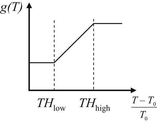
where c1, c2, c3, and c4, are weight factors and wl, area, and iv are, respectively, the normalized wirelength, area, and number of intertier vias [351]. The last term is a cost function to represent the temperature. An example of this function is a ramp function of the temperature, as shown in Fig. 13.1. Note that the cost function does not intersect the abscissa but, rather, the plateaus. Consequently, this objective function does not minimize the temperature of the circuit but, rather, constrains the temperature within a specified level. Indeed, minimizing the circuit temperature may not be an effective objective, leading to prohibitively long computational times or failure to satisfy other design objectives.
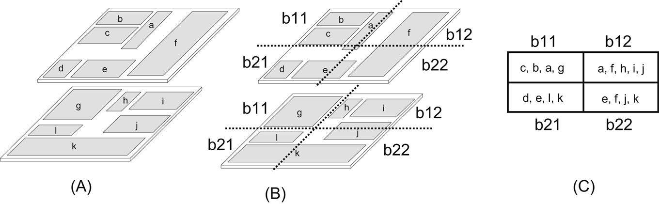
As with thermal unaware floorplanning techniques, the choice of floorplan representation also affects the computational time. Sequence pair and corner block list representations have been used for 3-D floorplanning, as discussed in Chapter 9, Physical Design Techniques for Three-Dimensional ICs. In addition to these approaches, a low overhead scheme is realized by representing the blocks within a 3-D system with a combination of 2-D matrices that correspond to the tiers of the system and a bucket structure that contains the connectivity information for the blocks located on different tiers (a combined bucket and 2-D array (CBA)) [351]. A transitive closure graph describes the intratier connections of the circuit blocks. The bucket structure can be envisioned as a group of buckets imposed on a 3-D stack. The indices of those blocks that intersect a bucket are included, irrespective of the tier on which a block is located. A 2×2 bucket structure applied to a two tier 3-D IC is shown in Fig. 13.2, where the index of the bucket is also depicted. To explain the bucket index notation, consider the lower left tile of the bucket structure shown in Fig. 13.2C (i.e., b21). The index of the blocks that intersects with this tile on the second tier is d and e, and the index of the blocks from the first tier is l and k. Consequently, b21 includes d, e, l, and k.
Simulated annealing (SA) is employed to optimize an objective function, as in (13.1) for thermal floorplanning of 3-D circuits. The SA scheme converges to the desired freezing temperature through several solution perturbations. These perturbations include one of the following operations, some of which are unique to 3-D ICs:
3. intratier reversal of the position of two blocks;
4. move of a block within a tier;
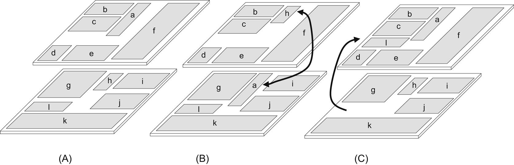
The last three operations are unique to 3-D ICs, while the z-neighbor swap can be treated as a special case of intertier swapping of two blocks. Therefore, two blocks located on adjacent tiers are swapped only if the relative horizontal distance between these two blocks is small. In addition, the z-neighbor move considers the move of a block to another tier of the 3-D system without significantly altering the x-y coordinates. Examples of these two operations are illustrated in Fig. 13.3.
Moreover, every time a solution perturbation occurs, the cost function is reevaluated to gauge the quality of the new candidate solution. Computationally expensive tasks, such as wirelength and temperature calculations, are therefore invoked. To avoid this exhaustive approach, incremental changes in wirelength for only the related blocks and interconnections are evaluated, as applied to the techniques described in Chapter 9, Physical Design Techniques for Three-Dimensional ICs. Note that the thermal profile of the heat diffusion can change the temperature across an area that extends beyond the recently moved blocks.
Consequently, each block perturbation requires the thermal profile of a 3-D circuit to be determined. This strict requirement, however, can increase the computational time, becoming a bottleneck for temperature related physical design techniques. A thermal profile, therefore, is invoked only after a specific operation or after a specified number of iterations. The reason behind this practice is that not all operations significantly affect the temperature of an entire system; rather, only a portion of the system. For example, intratier moves of two small area blocks or the rotation of a block are unlikely to significantly affect the temperature of a system, whereas other operations, such as a z-neighbor swap or a z-neighbor move, can significantly affect the temperature of the tiers and, more broadly, the entire system.
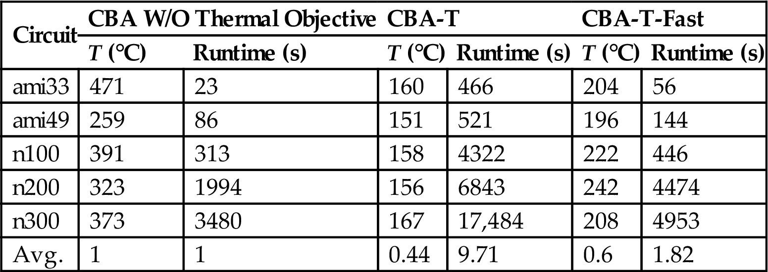
Thermal analysis techniques to determine the temperature of a 3-D circuit, each with different levels of precision and efficacy, can be applied, as discussed in Chapter 12, Thermal Modeling and Analysis. To ascertain the effects of different thermal analysis approaches on the total time of the thermal floorplanning process, thermal models with different accuracy and computational time have been applied to MCNC benchmarks in conjunction with this floorplanning technique. These results are reported in Table 13.1, where a compact thermal modeling approach is considered. A significant tradeoff between the computational runtime and the decrease in temperature exists between these thermal models. With thermal driven floorplanning, a grid of resistances is utilized to thermally model a 3-D circuit, exhibiting a 56% reduction in temperature [351]. The computational time, however, is increased by approximately an order of magnitude as compared to conventional floorplanning algorithms. Alternatively, if a closed-form expression is used for the thermal model of a 3-D circuit, the decrease in temperature is only 40%. The computational time is, however, approximately doubled in this case. Other design characteristics, such as area and wirelength, do not significantly change between the two models.
Table 13.1
Decrease in Temperature Through Thermal Driven Floorplanning [351]
| Circuit | CBA W/O Thermal Objective | CBA-T | CBA-T-Fast | |||
| T (°C) | Runtime (s) | T (°C) | Runtime (s) | T (°C) | Runtime (s) | |
| ami33 | 471 | 23 | 160 | 466 | 204 | 56 |
| ami49 | 259 | 86 | 151 | 521 | 196 | 144 |
| n100 | 391 | 313 | 158 | 4322 | 222 | 446 |
| n200 | 323 | 1994 | 156 | 6843 | 242 | 4474 |
| n300 | 373 | 3480 | 167 | 17,484 | 208 | 4953 |
| Avg. | 1 | 1 | 0.44 | 9.71 | 0.6 | 1.82 |
As the block operations allow intertier moves, exploring the solution space becomes a challenging task [352]. To decrease the computational time, floorplanning can be performed in two separate phases. In the first step, the circuit blocks are assigned to the tiers of a 3-D system to minimize area and wirelength, effectively ignoring the thermal behavior of the circuit during this first stage. This phase, however, can result in highly unbalanced power densities among the tiers. A second step that limits these unbalances is therefore necessary. An objective function to accomplish this balancing process is [496]
(13.2)
where c5, c6, c7, c8, and c9 notate weighting factors. Beyond the first two terms that include the area and wirelength of the circuit, the remaining terms consider other possible design objectives for 3-D circuits. The third term minimizes the imbalance that can exist among the dimensions of the tiers within the stack, based on the deviation dimension approach described in [350]. Tiers with particularly different areas or greatly uneven dimensions can result in a significant portion of unoccupied silicon area on each tier.
The last two terms in (13.2) consider the overall power density within a 3-D stack. The fourth term considers the power density of the blocks within the tier as in a 2-D circuit. Note that the temperature is not directly included in the cost function but is implicitly captured through management of the power density of the floorplanned blocks. The cost function characterizing the power density is based on a similarly shaped function as the temperature cost function depicted in Fig. 13.1. Thermal coupling among the blocks on different tiers is considered by the last term and is
(13.3)
 (13.3)
where Pi is the power density of block i, and Pij is the power density due to overlapping block i with block j from a different tier. The summation operand adds the contribution from the blocks located on all of the other tiers other than the tier containing block j. If a simplified thermal model is adopted, an analytic expression as in (13.3) captures the thermal coupling among the blocks, thereby compensating for some loss of accuracy originating from a crude thermal model.
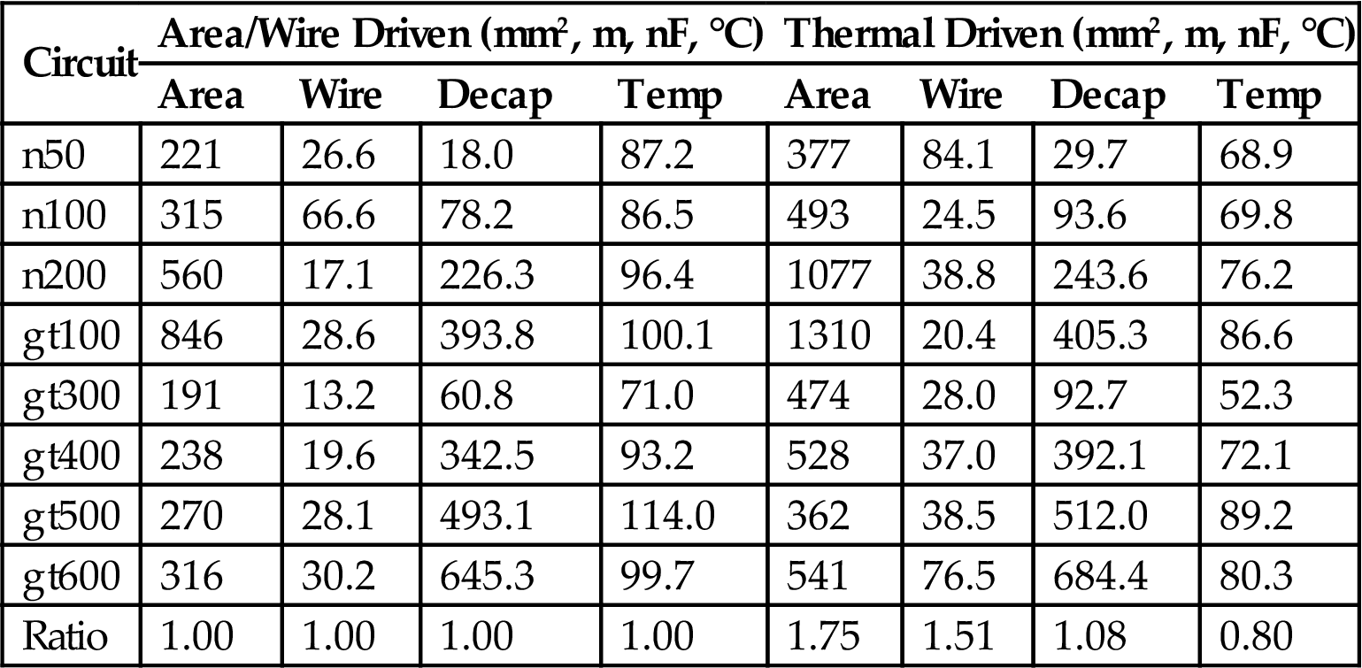
This two step floorplanning technique has been applied to several Alpha microprocessors [499]. Results indicate a 6% average improvement in the maximum temperature as compared to 3-D floorplanning without a thermal objective [496]. In addition, comparing a 2-D floorplan with a 3-D floorplan, an improvement in area and wirelength of, respectively, 32% and 50% is achieved [496]. The peak temperature, however, increases by 18%, demonstrating the importance of thermal issues in 3-D ICs.
The reduction in temperature is smaller than the one step floorplanning approach. Alternatively, for a two step approach, the solution space is significantly smaller, resulting in decreased computational time. The interdependence, however, of the intratier and intertier allocation of the circuit blocks is not captured, which can yield inferior solutions as compared to one step floorplanning techniques.
SA methods have also been employed for floorplanning modules in SoP (see Section 2.2), which is another variant of 3-D integration with coarse granularity. A cost function similar to (13.2) includes the decoupling capacitance and temperature in addition to area and wirelength. The modules in each tier of the SOP are represented by a sequence pair to capture the topographical characteristics of the SOP. To avoid the computational overhead caused by thermal analysis of the SOP during SA iterations, an approximation of the thermal profile of the circuit is used.
The temperature for an initial floorplan of the SoP is produced using the method of finite differences. The finite difference approximation given by (12.3) can be written as RP=T, where R is the thermal resistance matrix. The elements of the thermal matrix contain the thermal resistance (or conductance) between two nodes in a 3-D mesh, while the temperature T and power vector P contain, respectively, the temperature and power dissipation at each node. Any modification to the placement of the cells causes all of these matrices to change. To determine the resulting change in temperature, the thermal resistance is updated and multiplied with the power density vector. This approach, however, leads to long computational times. Consequently, assuming the modules in the SoP exhibit similar thermal conductivities dominated by the volume of silicon, the thermal resistance matrix is not updated, although any module move results in some change in the matrix.
Only local changes in the power densities due to a move of a module are considered. Consequently, for each modification of the block placement, the change in the power vector ΔP is scaled by R, and the change in the temperature vector is evaluated. A new temperature vector is obtained after the latest move of the blocks within a 3-D system. Results from applying this thermally aware SoP floorplanning technique are listed in Table 13.2, where the results from a placement based on traditional area and wirelength objectives are also provided for comparison [397].
Table 13.2
Thermal Driven Floorplanning for Four Tier 3-D ICs [397]
| Circuit | Area/Wire Driven (mm2, m, nF, °C) | Thermal Driven (mm2, m, nF, °C) | ||||||
| Area | Wire | Decap | Temp | Area | Wire | Decap | Temp | |
| n50 | 221 | 26.6 | 18.0 | 87.2 | 377 | 84.1 | 29.7 | 68.9 |
| n100 | 315 | 66.6 | 78.2 | 86.5 | 493 | 24.5 | 93.6 | 69.8 |
| n200 | 560 | 17.1 | 226.3 | 96.4 | 1077 | 38.8 | 243.6 | 76.2 |
| gt100 | 846 | 28.6 | 393.8 | 100.1 | 1310 | 20.4 | 405.3 | 86.6 |
| gt300 | 191 | 13.2 | 60.8 | 71.0 | 474 | 28.0 | 92.7 | 52.3 |
| gt400 | 238 | 19.6 | 342.5 | 93.2 | 528 | 37.0 | 392.1 | 72.1 |
| gt500 | 270 | 28.1 | 493.1 | 114.0 | 362 | 38.5 | 512.0 | 89.2 |
| gt600 | 316 | 30.2 | 645.3 | 99.7 | 541 | 76.5 | 684.4 | 80.3 |
| Ratio | 1.00 | 1.00 | 1.00 | 1.00 | 1.75 | 1.51 | 1.08 | 0.80 |
Although SA is the dominant optimization scheme used in most floorplanning and placement techniques for 3-D ICs [351,397,409], thermal aware floorplanners based on the force directed method have also been investigated. The motivation for employing this method stems from the lack of scalability of the SA approach. The analytic nature of force directed floorplanners, however, formulates the floorplanning problem into a continuous 3-D space. A transition is required between placement in the continuous volume and assignment without overlaps (i.e., legalization) within the discrete tiers of a 3-D system, potentially leading to a nonoptimal floorplan. In addition, as block level floorplanning includes components of dissimilar sizes, a different solution process is required as compared to floorplanning at the standard cell level [500].
This process includes more stages as compared to a traditional force directed method, as discussed in Chapter 9, Physical Design Techniques for Three-Dimensional ICs, due to legalization issues that can result during tier assignment. The different stages of the method are illustrated in Fig. 13.4, which are distinguished as (1) temperature aware lateral spreading, (2) continuous global optimization, and (3) optimization and tier assignment among the tiers within the 3-D stack. Assuming that the floorplan is a set of blocks {m1, m2, …, mn}, the method minimizes (1) the peak temperature Tmax of the circuit, (2) the wirelength, and (3) the circuit area, the product of the maximum width and height of the tiers within the 3-D stack. Each block mi is associated with dimensions Wi and Hi, area Ai=Wi × Hi, aspect ratio Hi/Wi, and power density Pmi. The height of the blocks is a multiple of the thickness of the tiers, which is assumed to be D for all of the physical tiers and L tiers are assumed to comprise the 3-D stack. A valid floorplan is an assignment of non-overlapping blocks within a 3-D stack, where the position of each block is described by (xi, yi, li), denoting the horizontal coordinate of the lower left corner of the block and tier li.
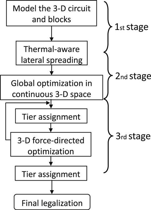
The continuous 3-D space within which the blocks are allowed to move and rotate consists of homogeneous cubic bins. The height of these bins is set to D/2, and the other two dimensions are half the size of the minimum block size. To determine the length of the connections between blocks, the half perimeter wirelength (HPWL) model is utilized. Based on this structure, two different forces are exerted on the blocks, where the aim of a filling force Ff is to remove overlaps, while a thermal force Fth reduces the resulting peak temperature. A filling force is formed for each bin by considering the density of the blocks within this bin. This density is determined for each bin based on the sum of the blocks covering a bin. Having determined all of the forces for each bin, the filling force applied to each block is equal to the summation of the forces related to all of the bins occupied by this block. Alternatively, the thermal force is based on the thermal gradient within the 3-D space. Obtaining the thermal gradients requires thermal analysis of the system, which in [500] is achieved through a spatially adaptive thermal analysis package [501].
The combination of these forces is the total force exerted on each block in each physical direction. Similar to (9.14), a system of equations is solved, for which the total force applied to the blocks in the x-direction is
(13.4)
where ax and βx are weighting parameters. Parameter ax controls the significance of the wirelength, area, and thermal objectives. Equivalently, βx characterizes the relative importance between the two forces in each direction. All of these parameters are empirically determined.
Having determined the forces on each block, the floorplanning process begins by spreading the blocks laterally within an xy-plane rather than the entire 3-D space. This spreading is at odds with traditional force directed methods where the blocks collapse at the center of the floorplan with high overlaps (see Chapter 9, Physical Design Techniques for Three-Dimensional ICs). As this situation results in strong filling forces, allowing the blocks to scatter throughout the 3-D space causes some large blocks to move to the boundary of the 3-D space, for example, close to the tier adjacent to the heat sink. A consequence of this practice can be a poor initial floorplan subjected to hot spots. Alternatively, spreading the blocks only in the xy-plane initially avoids this situation while simultaneously reducing the strong filling forces. Furthermore, this initial lateral spreading more evenly distributes the thermal densities, offering an initial distribution of the interconnect.
The second stage follows with global placement of the blocks within the volume of the system based on the filling and thermal forces. An issue that arises during this step is determining the thermal forces, which requires a thermal analysis of the circuit. As the thermal tool to perform this task is based on a tiered structure [501], a continuous floorplan is temporarily mapped into a discrete space. The temperature map for each tier is produced, and the thermal forces ensure that the global placement in continuous space can proceed. The global placement iterates until the overlap between the blocks is reduced to 5 to 10%.
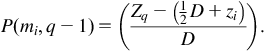
An approach to this interim tier mapping can be implemented stochastically, where the goal is to allocate the power density of the blocks to a specific tier to thermally analyze the system [500]. Considering that the center of block mi with coordinates (xi, yi, zi) is located between tiers q and q−1 during an iteration of the global placement, this block is placed within tier q or q−1 with a probability of, respectively,
(13.5)
 (13.5)
(13.6)
 (13.6)
Accordingly, the probability for a power density of block mi to be allocated to tier q or q−1 is, respectively,
(13.7)
(13.8)
Having produced a floorplan in a continuous 3-D space, tier assignment is realized. If this task takes place as a postprocessing step, however, inferior results can be produced. Instead, a third stage is introduced, as shown in Fig. 13.4, where tier assignment is integrated with floorplanning in a 2.5-D domain. As shown in Fig. 13.5 illustrating a continuous floorplan, a tier assignment of block 2 in either the first or second tier results in a different level of overlap in blocks 1 and 3. This overlap guides the force directed method with the tier assignment to ensure that the global placement produced by the previous stage is not significantly degraded.

This approach reduces the significant mismatches that can occur during tier assignment. Although these mismatches are often resolved as a postprocessing step, the heterogeneity of the shapes and sizes of the blocks can lead to significant degradation from the optimum placement produced during the second stage. Consequently, by integrating the tier assignment with the force directed method, these disruptive changes can be avoided.
The final step of the technique removes any remaining minor overlaps between blocks, where rotating the blocks has been demonstrated to improve the results as compared to moving the blocks within each tier. The topographical relationship among the blocks is captured in addition to the orientation of the blocks [502]. Although this technique is not based on a fixed outline, a boundary is assumed during legalization to detect an increase in the area of a tier, which can, in turn, cause an undesirable area imbalance. These violations are treated as additional overlaps. Additional moves and rotations are performed to remove these overlaps.
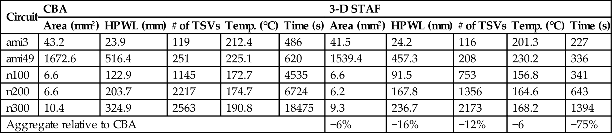
This force directed method has been compared to the SA based approach where CBA is employed. Some results are listed in Tables 13.3 and 13.4. In Table 13.3, the two methods are compared without considering thermal issues. The results indicate that the force directed method produces comparable results with CBA in area and number of through silicon vias (TSVs) but exhibits a decrease in wirelength. More importantly, the computational time is reduced by 31% [500]. If the thermal objective is added to the floorplanning process, the force directed method performs better in all of the objectives with a greater reduction in computational time than reported in Table 13.4. Note, however, that if the dependence between power and temperature is included in the thermal analysis process, the savings in time is significantly lower.
Table 13.3
Comparison for Area and Wirelength Optimization [500]
| Circuit | CBA | 3-D Scalable Temperature Aware Floorplanning (STAF) (No Temperature) | ||||||
| Area (mm2) | HPWL (mm) | # of TSVs | Time (s) | Area (mm2) | HPWL (mm) | # of TSVs | Time (s) | |
| ami3 | 35.30 | 22.5 | 93 | 23 | 37.9 | 22.0 | 122 | 52 |
| ami49 | 1490.00 | 446.8 | 179 | 86 | 1349.1 | 437.5 | 227 | 57 |
| n100 | 5.29 | 100.5 | 955 | 313 | 5.9 | 91.3 | 828 | 68 |
| n200 | 5.77 | 210.3 | 2093 | 1994 | 5.9 | 168.6 | 1729 | 397 |
| n300 | 8.90 | 315.0 | 2326 | 3480 | 9.7 | 237.9 | 1554 | 392 |
| Aggregate relative to CBA | +4% | −12% | −1% | −31% | ||||

Table 13.4
Comparison for Temperature Optimization [500]
| Circuit | CBA | 3-D STAF | ||||||||
| Area (mm2) | HPWL (mm) | # of TSVs | Temp. (°C) | Time (s) | Area (mm2) | HPWL (mm) | # of TSVs | Temp. (°C) | Time (s) | |
| ami3 | 43.2 | 23.9 | 119 | 212.4 | 486 | 41.5 | 24.2 | 116 | 201.3 | 227 |
| ami49 | 1672.6 | 516.4 | 251 | 225.1 | 620 | 1539.4 | 457.3 | 208 | 230.2 | 336 |
| n100 | 6.6 | 122.9 | 1145 | 172.7 | 4535 | 6.6 | 91.5 | 753 | 156.8 | 341 |
| n200 | 6.6 | 203.7 | 2217 | 174.7 | 6724 | 6.2 | 167.8 | 1356 | 164.6 | 643 |
| n300 | 10.4 | 324.9 | 2563 | 190.8 | 18475 | 9.3 | 236.7 | 2173 | 168.2 | 1394 |
| Aggregate relative to CBA | −6% | −16% | −12% | −6 | −75% | |||||
In addition to analytic techniques, other less conventional approaches to floorplan 3-D circuits have been developed. These approaches include genetic algorithms where, as an example, the thermal aware mapping of 3-D systems that incorporate a network-on-chip (NoC) architecture [503]. Merging 3-D integration with NoC is expected to further enhance the performance of interconnect limited ICs (the opportunities that emerge from combining these two design paradigms are discussed in Chapter 20, 3-D Circuit Architectures).
Consider the 3-D NoC shown in Fig. 13.6. The goal is to assign the tasks of a specific application to the processing elements (PEs) of each tier to ensure that the temperature of the system and/or communication volume among the PEs is minimized. The function that combines this objective characterizes the fitness of the candidate chromosomes (i.e., candidate mappings), described by
(13.9)

As with traditional genetic algorithms, an initial population is generated [504]. Crossover and mutation operations generate chromosomes, which survive to the next generation according to the relative chromosomal fitness. The floorplan with the highest fitness is selected after a number of iterations or if the fitness cannot be further improved.
13.1.2 Thermal Driven Placement
Placement techniques can also be enhanced by the addition of a thermal objective. The force directed method used in cell placement [371] and discussed in Section 9.3.1 has been extended to incorporate the thermal objective during the placement process [505] of standard cells in 3-D systems. In this approach, repulsive forces are applied to those cells that exhibit high temperatures (i.e., “hot blocks”) to ensure that the high temperature cells are placed at a greater distance from each other. The applied forces comprise both thermal forces and overlap forces. Since the objective is to reduce the temperature, the thermal forces are set equal to the negative of the thermal gradients. This assignment places the blocks far from the high temperature regions.
Determining these gradients, as discussed in the previous section, is a critical step of any temperature aware technique. Another method to obtain the temperature of a 3-D circuit is the finite element method [505]. The 3-D stack is discretized into a mesh consisting of unit cells, as discussed in Section 12.3. The thermal gradient of a point or node of an element is determined by differentiating the temperature vector along the different directions,
(13.10)
 (13.10)
Exploiting the thermal electric duality, the modified nodal technique in circuit analysis [473], where each resistor contributes to the admittance matrix (i.e., matrix stamps), is utilized to construct element stiffness matrices for each element. These elemental matrices are combined into a global stiffness matrix for the entire system, notated as Kglobal. This matrix is included in a system of equations to determine the temperature of the nodes that characterizes the entire 3-D circuit. The resulting expression is
(13.11)
where P is the power consumption vector of the grid nodes. To determine this vector, the power dissipated by each element of the grid is distributed to the closest nodes. From solving (13.11), the temperature of each node is determined during each iteration of the force directed algorithm. The thermal forces can be determined from the thermal gradient between grid nodes, requiring the following expression to be solved,
(13.12)
where fi is the force vectors in the x, y, and z directions. Matrix C describes the cost of a connection between two nodes, as defined in [371].
After the stiffness matrices are constructed, an initial random placement of the circuit blocks is generated. Based on this placement, the initial forces are computed, permitting the placement of the blocks to be iteratively determined. This recursive procedure progresses as long as an improvement above some threshold value is exhibited. The procedure includes the following steps [505]:
1. the power vector resulting from the new placement is determined;
2. the temperature profile of the 3-D stack is calculated;
3. the new value of the thermal and overlap forces is evaluated;
After the algorithm converges to a final placement, a postprocess step follows. During this step, the circuit blocks are positioned without any overlap within the tiers of the system. If one tier is packed, the remaining cells, initially destined for this tier, are positioned onto an adjacent tier. A similar process takes place in the y-direction to ensure that the circuit blocks are aligned into rows. A divide and conquer method is applied to avoid any overlap within each row. A final sorting step in the x-direction includes a postprocessing procedure, after which no overlap among cells should exist.
The efficiency of this force directed placement technique has been evaluated on MCNC [396] and IBM-PLACE benchmarks [506], demonstrating a 1.3% decrease in average temperature, a 12% reduction in maximum temperature, and a 17% reduction in average thermal gradient. The total wirelength, however, increases by 5.5%. This technique achieves a uniform temperature distribution across each tier, resulting in a significant decrease in thermal gradients as well as maximum temperature. The average temperature throughout a 3-D IC, however, is only slightly decreased. This technique, consequently, focuses on mitigating hot spots across a multi-tier system.
In all of the techniques presented in this section, the heat is transferred from the upper tiers to the bottom tier primarily through the power and signal lines and the thin silicon substrates of the upper tiers. No additional means other than redistributing the major heat sources throughout the 3-D stack lessens any significant thermal gradients. Furthermore, these techniques typically assume the power density associated with each module, block, or cell is temporally fixed. However, thermal management is also applicable in real-time, where power densities are monitored and adjusted to prevent the appearance of hot spots that affect circuit performance and contribute to aging, degrading the reliability of the system. These methods are described in the following section.
13.1.3 Dynamic Thermal Management Techniques
Thermal management techniques during circuit operation—typically used in processors—have received significant attention since around 2000 due to increasing power densities. The advent of multi-core architectures has further fueled interest in these techniques as each core within a processor is managed separately, offering several ways to thermally manage these complex computing systems. Although techniques for dynamic power management exist [507], simply reducing power is not sufficient due to the thermal coupling of circuits and spatially varying thermal conductivities across a system. Decreasing power can lower the peak or average temperature of an integrated system, yet the thermal gradients may be higher if appropriate thermal management techniques are not applied. The appearance of hot spot(s) in some region(s) of a circuit can be attributed to the inability of power reduction techniques to eliminate these thermal gradients despite the average temperature of the circuit being maintained within thermal limits.
Dynamic thermal management (DTM) methods can be applied to both software and hardware, where a combination of techniques is often used. In hardware, dynamic frequency voltage scaling (DVFS) and clock gating (or throttling) are commonplace techniques, while in software, workload (or thread) migration is usually employed to cool down cores [508]. The granularity at which thermal policies are applied can also vary, in particular, for multi-core processors. For example, a single voltage/frequency pair can be chosen for an entire processor (a global policy) or each core may have a separate voltage/frequency depending upon the temperature of the core (a distributed policy).
A number of tradeoffs exist among these choices, leading to a relatively broad design space for dynamic thermal management. Software methods (driven by the operating system) are usually coarse grained methods and are less effective than hardware techniques since the latter can respond faster to alleviate steep transient thermal loads. Software methods can, however, be implemented relatively easily by scheduling tasks among the different parts of a system. In a multi-core system, threads are swapped among processors or assigned to different processors depending upon the temperature of each core, where these changes typically take place at tens of milliseconds [509,510]. Several techniques use a 10 ms interval for job scheduling as this interval is also used in the Linux kernel for timer interrupts [509]. DVFS mechanisms are more complex to implement. This complexity increases if a distributed (per core) DVFS scheme is employed. Despite the greater complexity, however, these techniques are widely used in modern processors to maintain the temperature within specified limits [511,512].
Determining the temperature of a circuit during operation is another important aspect of dynamic thermal management as slow responses can render these techniques inefficient or excessively strict. Different means are used to determine the temperature of a circuit including thermal sensors [512] and performance counters that characterize a core, such as accesses to register files, cycle counts, and number of executed instructions [508]. Information from thermal sensors is used directly, where the primary issue for sensors is the response time to changes in temperature, recognizing that thermal constants within integrated systems are typically on the order of milliseconds. Thermal sensors constitute a reliable means for measuring circuit temperature to guide a thermal management policy. Alternatively, the information from performance counters is loosely connected to temperature and, although widely explored in the literature, outputs from these components represent a proxy and should be used with caution [509].
Less complex dynamic thermal policies are also available, where the online workload schedule is based on the thermal profile of the target system obtained offline for the expected combination of workloads [513]. This strategy reduces the overhead of thermal management; the efficiency, however, may be lower than fully online methods. These methods are particularly effective for those scenarios where the workload combinations differ from those workloads employed during offline energy profiling of the system.
Several efforts employing dynamic thermal management approaches, both in software and hardware, have been published [497,508, 510–512]. Similarly, several works pay attention to the design and allocation of thermal sensors within 2-D circuits [514]. Although these techniques can also be applied to 3-D circuits, the resulting efficiency may not be similar. This drop in efficiency can be attributed to the strong thermal coupling between adjacent circuits. This coupling is more pronounced in the vertical direction due to the significantly smaller physical distance between circuits and that heat primarily flows in the vertical direction. Other reasons for developing novel thermal policies for 3-D systems include the case where memory (e.g., DRAM) tiers are stacked on top of a processor tier [515]. Although the processor tier is located next to the heat sink, care must be placed to ensure processor operation does not cause the temperature to rise beyond the strict thermal limits of DRAM [516]. Higher overall power can occur due to more frequent refreshing of the stored data. The remainder of this section reviews the evolution of thermal management techniques for 3-D systems, emphasizing either multi-tier processor architectures or a combination of a processor tier vertically integrated with tiers of memory.
13.1.3.1 Dynamic thermal management of three-dimensional chip multi-processors with a single memory tier
Although automatic control theory has been used to guide workload scheduling for thermal management [508], most techniques are based on heuristics due to low complexity characteristics. A heuristic OS-level scheduling algorithm targeting 3-D processors has been proposed in [498]. The key concept of this technique is to consider the strong thermal coupling along the vertical direction in the scheduling process to balance temperatures across the stack, thereby reducing thermal gradients and decreasing the frequency in those cores with hot spots. The occurrence of hot spots requires aggressive thermal measures which degrade system performance. Consider a 3-D multi-core system. The assumption is that irrespective of the floorplan, which can also be thermally driven, leading to the stacking of energy demanding cores with low power caches, stacking of cores may be unavoidable. In this case, careful scheduling lowers the temperature of the system, where the scheduling process considers the entire stack rather than individual tiers. Assigning tasks to those cores situated in the tier next to the heat sink should, therefore, not be based on the temperature of a specific tier (which is lower than in other tiers) but, rather, the temperature of those cores in tiers farther away.
Due to the vertical thermal coupling, rather than assigning a single task to one core, a stack of cores (for example, an entire 3-D system split into several pillars of cores) is considered, where a task is assigned to every processor within this stack. The terms, “super-core” and “super-tasks,” are used to describe the main features of the heuristic. Assuming a 3-D system with n tiers and m cores per tier, the tasks on n×m cores require scheduling. With this notation, a super-core consists of n cores, where a task is assigned to each core to distribute a balanced temperature. The assignment process forms super-tasks that require comparable power. These super-tasks are assigned to each super-core.
To balance the power across the super-cores, the power of all of the (n×m) tasks is sorted. Each task and associated power are assigned to the available m bins (of super-tasks). The assignment proceeds iteratively by inserting power values, in descending order, to that bin with the smallest total power during this iteration. The process continues until every task has been assigned to a bin. An example assignment is shown in Fig. 13.7, where sorting of power within tasks and the resulting task assignment to four bins are depicted for a twotier 3-D system containing four cores per tier. As the main operation of this heuristic is sorting, the time complexity is O(mnlog(mn)) [498].

In addition to task scheduling, DVFS within each super-core is assumed, although DVFS for a core is not necessarily straightforward. Thus, if a core exceeds a thermal threshold, DVFS scales the voltage supply of the core with the highest power (which may or may not be the overheated core within a super-core). The objective is to penalize the task that consumes the highest power, which may cause overheating in a vertically adjacent core. DVFS is applied to only one core within a super-core, which limits the benefits of this technique.
Job scheduling is applied to the benchmark suite of applications, SPEC2000 [517], where several workloads are combined to form benchmark sequences with diverse power profiles and thermal loads. For example, thermal analysis of the crafty and mcf workloads yields a HC (hot-cold) scenario. These workloads are applied to a 3-D multi-core architecture with two tiers and four cores per tier, where a P4 Northwood architecture operating at 3 GHz is assumed for each core.
To evaluate the effectiveness of the heuristic, other task assignments have also been considered. The baseline for comparison is a random assignment of tasks to cores based on the Linux 2.6 scheduler [509]. The scheduler works similarly to Linux but with a slightly smaller scheduling interval of 8 ms. A round robin scheduler is also utilized for comparison. Finally, another scheduling approach, where the objective is to balance temperature by assigning a high power task to a cool core but without considering the temperature of the vertically adjacent cores, is also evaluated for the purposes of comparison.
A comparison in terms of peak temperature among these task scheduling methods for the target workload scenarios demonstrate that the heuristic assignment reduces the peak temperature by up to 24°C as compared to a random assignment. Other techniques similarly decrease the peak temperature. Thermal coupling in task scheduling supports the removal of a large number of thermal problems when DVFS is employed. DVFS, however, often counteracts the benefits of job scheduling as DVFS requires a greater performance overhead.
In contrast to the method described in [498], where frequent use of DVFS is avoided, other techniques consider combining both software and hardware techniques. The objective of these methodologies is to balance the effectiveness of each technique against the overhead without favoring one technique over the other. Thus, a thermal management framework has been developed for 3-D chip multi-processors (CMP), where clock gating, DVFS, and workload scheduling are all applied to satisfy thermal limits without degrading performance [497]. This goal is achieved by applying these techniques both in a distributed (or local) and global (or centralized) manner. A distributed approach provides greater versatility when applying a thermal policy as allowing DVFS only for a core within each super-core is a restricted approach. The structure and operation of this framework are discussed in the following subsection.
13.1.3.2 Software/hardware (SW/HW) thermal management framework for three-dimensional chip multi-processor
The development of this framework requires a set of tools for architectural, power, and thermal modeling. These tools include the M5 architectural simulator [518], a Wattch-based EV6 model [519], CACTI [520], the approach described in [521] for power modeling of the cores, caches, and leakage power, and a tool based on [522] for thermally analyzing these systems. Irrespective of the specific tools, architectural simulators, power models and/or simulators, and thermal analysis tools are all required to design and evaluate a dynamic thermal management policy for CMP or multi-processor system-on-chip (MPSoC) systems. The framework is based on specific guidelines, which are based on a first order thermal analysis of a two tier CMP, as illustrated in Fig. 13.8. In this example, the electrical-thermal duality is used to analyze the thermal behavior of a CMP, where each core is represented by a single node in an equivalent thermal model. Only a simple path for the heat to flow is assumed to exist within the stack. At first glance, the thermal conductivity of the cores in the upper tier (e.g., core I) is lower than the thermal conductivity of those cores in the lower tier, which implies that the temperature of core I is higher than in cores J and K. Additionally, thermal coupling between cores in the same tier (cores J and K) is considerably lower, implying comparable cooling efficiencies. These observations suggest that workload scheduling should consider the different cooling efficiencies of the cores and the effect that a workload can have on other cores within a system.
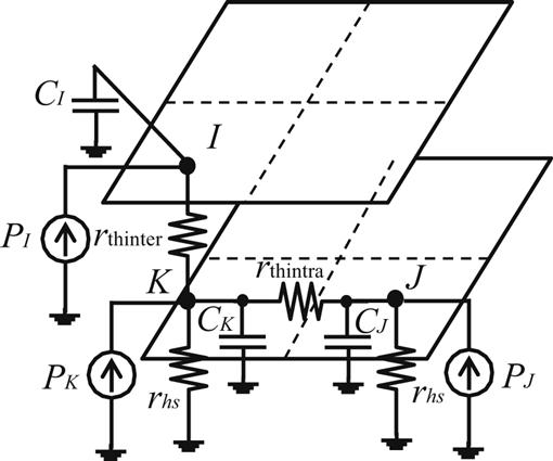
To extend this analysis to a CMP with m cores, specific data that affects the thermal behavior of the cores need to be determined. Consequently, the cooling efficiency of each core determines the workload schedule. The schedule is extracted from the steady-state heat conduction expression, T=PRth−1, where matrix Rth includes the thermal resistance connecting the nodes (i.e., cores) within the thermal model. Notating the temperature of core i as Ti, the temperature is
(13.13)
 (13.13)
where rthi,j is the thermal resistance between cores i and j, and pj is the power consumed by core j. The row i,j of matrix Rth describes the effect of the cores on the temperature at core i. Furthermore, considering the quadratic relationship between dynamic power consumption and voltage, and that the operating frequency exhibits a roughly linear dependence on voltage, power dissipation can be described as pj=si,j fj3 where fj is the operating frequency of core j. The term si,j is the product of the switching activity of the core multiplied by the switched capacitance, which is linearly proportional to the number of instructions per cycle (IPC) of the job being executed on core j. The figure of merit, thermal impact per performance (TIP), is introduced to formulate guidelines for the thermal control of 3-D CMPs,
(13.14)
(13.15)
which denotes the effect of core j on the temperature of core i, where the frequency fi (and voltage) through DVFS and the workload IPCj are assigned to core j.
Robust thermal management of a CMP is intended to improve performance while satisfying specific thermal constraints, which can vary among cores. A metric to describe the performance of a CMP is the total number of instructions per second executed by a CMP,
(13.16)
 (13.16)
The thermal constraints that apply to a CMP are determined by the thermal limit of each core, which is assumed to be equal for all cores. Consequently, the requirement is that ![]() . Satisfying this constraint requires equating the thermal impact per performance of all cores. This decision leads to assigning different frequencies among those cores with different cooling efficiencies, and executing jobs with different IPCs. This method results in two approximate design guidelines. For intertier processors, the frequencies and IPCs should be assigned based on the cooling efficiency of the cores, given by (13.13) to (13.16), where both the frequency and IPC are, in general, different. This guideline is in accordance with the heuristic described in [498], where the assignment of a workload to a core considers both the temperature as well as the location of a core within the stack. The capability to transfer heat to the ambient is affected by the power dissipated during an assigned workload. Alternatively, among cores situated within the same tier, where the cooling efficiency is roughly the same based on the thermal model of Fig. 13.8, the same frequency and workloads with similar IPC are assigned.
. Satisfying this constraint requires equating the thermal impact per performance of all cores. This decision leads to assigning different frequencies among those cores with different cooling efficiencies, and executing jobs with different IPCs. This method results in two approximate design guidelines. For intertier processors, the frequencies and IPCs should be assigned based on the cooling efficiency of the cores, given by (13.13) to (13.16), where both the frequency and IPC are, in general, different. This guideline is in accordance with the heuristic described in [498], where the assignment of a workload to a core considers both the temperature as well as the location of a core within the stack. The capability to transfer heat to the ambient is affected by the power dissipated during an assigned workload. Alternatively, among cores situated within the same tier, where the cooling efficiency is roughly the same based on the thermal model of Fig. 13.8, the same frequency and workloads with similar IPC are assigned.
These guidelines underpin the thermal management policy developed at the operating system level [497], where the temperature is obtained from the thermal sensors. Performance counters gather information for workload monitoring and to estimate the IPC. With this information and the aforementioned guidelines, this framework applies distributed workload migration and real-time thermal control, globally adapting the power and thermal attributes across CMPs.
At the global CMP (global) level, the power and thermal budgets are determined for each core using a hybrid online/offline technique. For each workload the optimal voltage/frequency pair is determined. The temperature of each workload is computed, and the power is updated to consider the dependence on temperature. The voltage/frequency (V/F) pair is chosen to satisfy the thermal limit. After several iterations, the temperature and temperature dependent power converge. The resulting V/F pair is stored in a look-up table. This table is integrated with the OS and is periodically invoked.
Thermal balancing is also leveraged by a distributed policy where the IPC of each core is monitored and, if required, adjusted to guarantee thermal safety. This adjustment is primarily between vertically adjacent cores, since greater thermal heterogeneity is noted. The workload migration swaps jobs to assign those workloads with high IPCs to those cores with higher cooling efficiencies. This migration of workloads takes place every 20 ms. If thermal transients, however, occur at faster rates, other thermal control measures are considered, such as DVFS and clock gating. These techniques are applied locally, thereby providing better control of thermal gradients across the stack as compared to a centralized approach. Moreover, due to the considerable impact on performance of clock gating, DVFS is the primary method. Clock gating is only used for thermal emergencies.
This framework is applied to a 3-D CMP consisting of three physical tiers. Two of these tiers host eight Alpha21264 cores (four in each tier) assuming a 90 nm CMOS node, and the third tier contains the L2 cache. A comparison of the framework with a strictly distributed thermal policy [508] for this 3-D CMP, where the simulated workloads are based on applications from SPEC2000 [517] and Media benchmark suites, exhibits an improvement of, on average, 30%. This situation is due to the strong thermal coupling of the vertically adjacent cores. Local control cannot capture this coupling since the workload and V/F pair are chosen for this core. Employing power and thermal budgeting at the global level can, however, address this limitation, improving the overall throughput of the CMP.
In addition to the cooling efficiency, an analysis of the characteristics of the workloads can yield greater performance of the CMP, assuming the same thermal limits [523]. To assess these improvements, the workloads are classified as compute bound or memory bound, depending upon the memory requirements of the workloads. Analyzing memory transfers between the core and in-stack memory provides useful information that can be included within the thermal policies. Considering that instructions are executed at a clock rate fCPU and the off-chip memory transfers due to L2 cache misses are performed at a clock rate foff-chip, the time to execute a task is [523],
(13.17)
where won-chip is the number of clock cycles to execute CPU instructions without a cache miss, and woff-chip is the number of clock cycles for external transfers if the core stalls. This simple expression describes whether a workload is compute bound (e.g., high won-chip) or memory bound (e.g., high woff-chip). Both of these quantities depend upon the type of application and the time needed for a core to execute an application. The off-chip clock rate is also considered constant, while the clock cycles for off-chip memory transfer are modeled as a function of the number of cache misses. woff-chip=(aNmiss+b)·fCPU is the number of L2 misses denoted by Nmiss [524]. The coefficients a and b are fixed and depend on the target architecture, while the number of misses is determined by performance monitors, such as PAPI [525].
Collection of this information can quantify the speed up required to execute a workload due to an increase in the core clock frequency (which affects the temperature). This speed up for each core and workload at two different frequencies is
(13.18)
This simple metric computes the gains in IPS for a workload with different core clock frequencies. These speed ups, however, cannot be exploited unless the temperature of the core is lower than the maximum temperature at the target frequency. Application of these higher frequencies is performed effectively if the instantaneous temperature rather than the steady state temperature (SST) of a core is employed. The use of the instantaneous temperature tracks the closeness of each core to the maximum allowed temperature and core frequency. This approach is not considered in [497] where the SST of a core determines the thermal effect on the cores and drives the workload allocation policy. Note that the term instantaneous temperature refers to the temperature of a core over several milliseconds, since thermal constants are orders of magnitude greater than the clock frequency.
A considerably lower instantaneous temperature, notated as Tinst from the maximum allowed temperature Tmax, provides a temperature slack [523] which can be exploited by operating the core at a higher frequency. Performance improvements can, therefore, be determined by SU for each workload. Thus, not only the cooling efficiency of each core but also the SU can improve the IPS of a 3-D CMP [523], as described by (13.16). These frequency adjustments of finer granularity should, however, be carefully performed due to the strong thermal coupling in the vertical direction. This coupling has a detrimental effect on the temperature of the other cores within the 3-D CMP, particularly those cores located in other tiers at the same 2-D position.
The optimization problem of maximizing (13.16) is solved subject to the constraint that the temperature of those cores farthest from the heat sink is equal to Tmax. Solving this optimization problem with the use of Laplace multipliers leads to the following expression applied to each core i [523],
(13.19)
where M is a constant. Determining the precise frequency for each core that satisfies (13.19), however, is not feasible since the clock frequency changes discretely. Only a small set of clock frequencies is supported by a CMP. Consequently, an approximate solution is offered to ensure that the frequency assigned to each core deviates the least from (13.19).
Solving (13.19) requires the thermal resistance Rthi, power Pi, and IPCi of each core i. The thermal resistance of each core in the CMP is illustrated in Fig. 13.8, while the power is determined by the IPC of the core. Allocation of the IPC to the cores for each workload proceeds according to the heuristic of Section 13.1.3.1, where an example is depicted in Fig. 13.7. Rather than explicit power values, the IPC of each workload matches the super-tasks (i.e., a set of tasks) to the super-cores of the CMP. This procedure is repeated and threads are migrated at regular intervals (of 100 ms) [523].
Several scenarios based on the benchmark applications SPEC2000/2006 [517] and ALPbench [526] are used to evaluate the efficiency of thread migration based on the instantaneous temperature of each core. These scenarios include workloads with high, low, and mixed IPCs denoted, respectively, as HIPC, LIPC, and MIPC. The SU of these benchmarks is also classified as high, low, and mixed, where the frequency of each core switches between 1 and 2 GHz. The resulting IPS for a 3-D CMP comprising two core tiers and one memory tier are compared for two different thread management approaches. The first approach follows from [497]. The HIPCs are assigned to those cores closer to the heat sink (3-DI) and to cores with a lower SST, setting the clock frequency of each core to ensure that the SST does not exceed Tmax (3-DI-SST). Alternatively, the thread allocation assigns core frequencies based on the temperature slack of each core (Ti(t)≤Tmax) (IT), and assigns the super-task with the highest sum of IPCs to the coolest super-core. The thread with the highest SU (3-DIS) is assigned to the core of each super-core located closest to the heat sink (3-DIS-IT). A comparison between these two thread allocation policies results in an average IPS improvement of 18.5% for those scenarios listed in Table 13.5. The temperature slack for 3-DIS-IT is much lower, demonstrating that most cores operate close to Tmax due to the higher frequency, yielding both a higher total IPS and power for each scenario.
Table 13.5
Average Power Dissipation (Pavg) and Average Temperature Slacks (Tslack) of 3-DIS-IT and 3-DI-SST [523]
| Benchmark Combination | 3-DI-SST | 3-DIS-IT | ||
| Pavg (W) | Tslack (°C) | Pavg (W) | Tslack (°C) | |
| hipc-hm | 91.63 | 7.29 | 123.40 | 2.46 |
| hipc-mm | 113.86 | 5.08 | 118.97 | 4.29 |
| hipc-lm | 99.00 | 6.95 | 104.63 | 6.02 |
| mipc-hm | 104.30 | 7.32 | 150.53 | 2.30 |
| mipc-mm | 105.94 | 5.17 | 115.32 | 4.25 |
| mipc-lm | 84.56 | 7.53 | 87.77 | 6.99 |
| lipc-hm | 69.98 | 10.44 | 70.14 | 10.40 |
| lipc-mm | 85.03 | 7.37 | 85.70 | 6.94 |
| lipc-lm | 119.34 | 5.74 | 124.64 | 4.85 |

13.1.3.2.1 Dynamic thermal management of three-dimensional chip multi-processors with multiple memory tiers
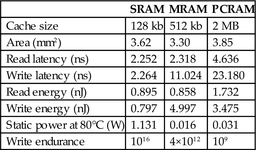
These techniques relate to CMPs when a single memory tier is considered. Adding more memory tiers improves performance as fewer cache misses occur; however, thermal management becomes a more acute issue as the distance of those tiers from the heat sink increases. The use of nonconventional memories, such as magnetic RAM [527], can alleviate this situation since a nonvolatile memory tier does not leak current, reducing the overall power of the stack. The introduction of these memory technologies requires different approaches for dynamic thermal management of 3-D CMPs since these memory technologies exhibit substantially different characteristics as compared to SRAM-based cache. For example, nonvolatile memories are slower and require higher energy to write, while the endurance is lower than SRAM. The main traits of different memory technologies are reported in Table 13.6.
Table 13.6
Parameters of Different Memory Technologies Fabricated in 65 nm Technology [529]
| SRAM | MRAM | PCRAM | |
| Cache size | 128 kb | 512 kb | 2 MB |
| Area (mm2) | 3.62 | 3.30 | 3.85 |
| Read latency (ns) | 2.252 | 2.318 | 4.636 |
| Write latency (ns) | 2.264 | 11.024 | 23.180 |
| Read energy (nJ) | 0.895 | 0.858 | 1.732 |
| Write energy (nJ) | 0.797 | 4.997 | 3.475 |
| Static power at 80°C (W) | 1.131 | 0.016 | 0.031 |
| Write endurance | 1016 | 4×10¹² | 109 |
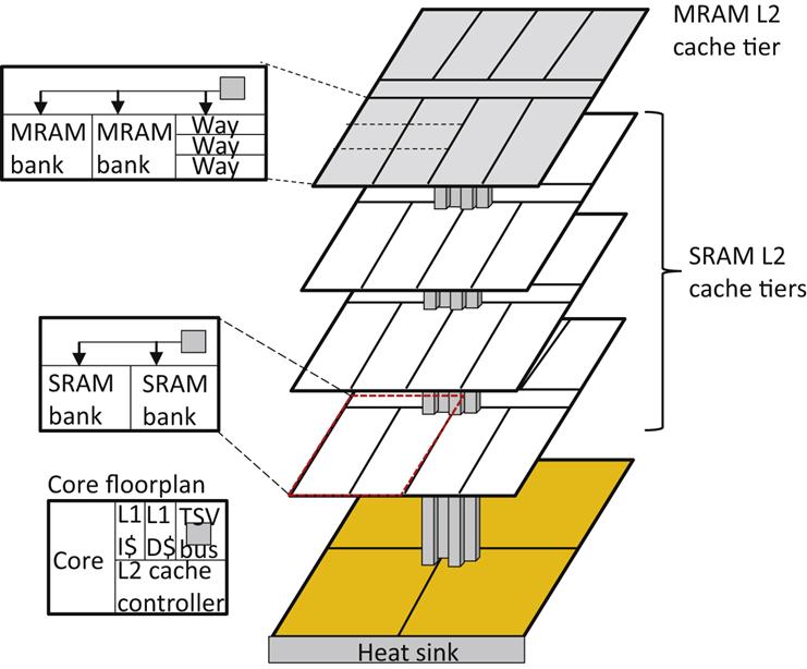
As magnetic memory is slower than SRAM, these memory tiers should be used to store less immediate data, while frequently accessed data or frequent write accesses should be placed within the SRAM tier. Considering a 3-D CMP that includes a mixture of memory tiers, an objective to improve the IPS of the CMP while satisfying thermal limits can be satisfied by power gating a cache at the “way-level” and applying DVFS for the cores of the CMP. An example of an architecture combining a mixture of memory technologies is shown in Fig. 13.9, where one processing tier with four cores is stacked with three tiers of SRAM and one tier of MRAM for L2 cache. L1 cache is integrated within the processing tier. The memory organization in each tier is also shown in the figure along with the vertical bus connecting the cache to the cores. The cores are connected through a crossbar switch (a large number of cores would require a NoC topology [528]). Allocation of the cache ways1 to each core lowers the temperature [527]. This allocation occurs dynamically both for the core and cache tiers where the leakage power of the memory tiers is also considered within the power budget. Key to this allocation strategy remains the notion of heterogeneous thermal coupling in the vertical direction throughout the entire stack, including the memory tiers.
To illustratively explain the concept behind the cache way and clock frequency allocation process, consider the example shown in Fig. 13.10. Five different schemes are applied to maximize IPS. In Fig. 13.10A, a low frequency clock (1 GHz) is chosen for both cores and cache ways allocated to each core from all of the SRAM tiers. As core 1 executes a memory demanding benchmark (Art), additional cache ways are provided to this core. The frequency cannot be substantially increased due to the greater power required by the L2 cache. In Fig. 13.10B, the clock frequency of both cores rises to 3 GHz but the cache available for each core is decreased to avoid excessive temperatures. Data would be lost and should therefore be transferred from main memory. In Fig. 13.10C, the clock of each core is adjusted through a DVFS mechanism, supporting a tradeoff between the capacity of the available L2 cache and the clock frequency. Replacing a tier of SRAM with MRAM (see Fig. 13.10D) and turning off some SRAM tiers supports a clock frequency of 3 GHz for both cores. Some data can be stored in the MRAM tiers, avoiding slow off-chip memory transfers, thereby achieving a better IPS than the system shown in Fig. 13.10B. Depending upon the workload, this hybrid-DVFS approach also employs DVFS to tradeoff the number of activated cache ways with clock frequency to ensure the resulting IPS of the 3-D CMP is maximized.

In the schemes shown in Figs. 13.10D and E, data stored in the MRAM tier are transferred into the faster SRAM tiers to limit the on-chip energy expended to transfer data from/to the memory. Data migration takes place with counters for each core that collect information on the least recently used and most recently used data blocks. This policy is implemented within the L2 memory controller [527]. Thus, a cache miss in the SRAM tier is compensated if a cache hit for this data occurs in the MRAM tier.
Maximizing IPS requires a set of parameters for both the cores and memory, including the clock frequency of each core, the number of SRAM and MRAM ways allocated to each core, and the number of activated SRAM and MRAM ways physically allocated on top of each core. This allocation occurs dynamically, where a configuration interval of 50 ms is employed [527]. Partition of the power gated memory blocks is also demonstrated in [530] but not to increase CMP throughput.
The IPS for the target 3-D architecture is analytically described in [527]. Two additional concepts are introduced to determine the number of cache ways allocated to each processor as well as which ways are activated. Consequently, the performance improvement (PI) of IPS in terms of the SRAM cache ways ![]() assigned to core i is
assigned to core i is
(13.20)
A similar expression applies to the cache ways of the MRAM, ![]() . Similar to PI, the performance loss (PL) incurred by the activation of one more cache way within a super-core
. Similar to PI, the performance loss (PL) incurred by the activation of one more cache way within a super-core ![]() , entails a decrease in clock frequency fi to maintain the temperature within specified limits,
, entails a decrease in clock frequency fi to maintain the temperature within specified limits,
(13.21)
 (13.21)
A similar expression applies for the cache ways of the active MRAM, ![]() . With PI, PL, and the Lagrange multipliers, the IPS reaches a maximum for a specific temperature if the SRAM and MRAM cache ways for each core are selected to ensure that PI and PL are equal among all cores. Greedy heuristic algorithms and the bisection method are typically utilized to determine the SRAM and MRAM cache ways allocated to each core as well as the number of active ways within a configuration interval. The number of active ways depends upon the clock frequency of the core and the maximum tolerated temperature.
. With PI, PL, and the Lagrange multipliers, the IPS reaches a maximum for a specific temperature if the SRAM and MRAM cache ways for each core are selected to ensure that PI and PL are equal among all cores. Greedy heuristic algorithms and the bisection method are typically utilized to determine the SRAM and MRAM cache ways allocated to each core as well as the number of active ways within a configuration interval. The number of active ways depends upon the clock frequency of the core and the maximum tolerated temperature.
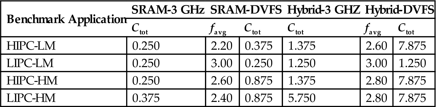
To demonstrate the efficiency of hybrid-memory and the performance benefits of the cache way allocation, a set of benchmarks is evaluated on the target architecture. The features of the memory tiers are listed in Table 13.6. The processor tier is based on the Intel Core i5 technology operating at 3 GHz. The benchmark applications are based on the SPEC2000/2006 and include combinations of workloads with HIPCs and low IPCs (LIPCs) as well as high memory (HM) and low memory (LM) demands (see Table 13.7). The schemes depicted in Figs. 13.10C–E are compared to the scheme where the cores operate at 3 GHz, SRAM is only used, and most of the cache ways are power gated to satisfy temperature requirements (Fig. 13.10B). The results of this comparison are reported in Table 13.8, where SRAM-DVFS (Fig. 13.10C) improves IPS by 26.7% and hybrid-DVFS exhibits an increase in IPS of, on average, 55.3%. Moreover, the energy-delay product (EDP) is also improved by 78.2% for SRAM-DVFS. This improvement is achieved by activating additional cache ways and using a lower clock frequency. The fewer cache misses allow the execution to finish earlier than SRAM-3 GHz, yielding improved EDP. Similarly, the hybrid-DVFS yields a lower EDP as compared to the hybrid-3 GHz of, on average, 32.1%.
Table 13.7
Combinations of Benchmark Applications to Compare the Performance of Different Thermal Management Schemes Based on SRAM/MRAM L2 Cache [527]
| Scenarios of Benchmark Applications | Benchmark Applications for Each Scenario |
| HIPC-LM | equake, parser |
| LIPC-LM | lbm, mcf06, sjeng, ammp |
| HIPC-HM | gcc, bzip |
| LIPC-HM | gcc, art |
Table 13.8
Average Clock Frequency favg (GHz) and Allocated L2 Cache Capacity Ctot (MB) for Each Thermal Management Scheme [527]
| Benchmark Application | SRAM-3 GHz | SRAM-DVFS | Hybrid-3 GHZ | Hybrid-DVFS | ||
| Ctot | favg | Ctot | Ctot | favg | Ctot | |
| HIPC-LM | 0.250 | 2.20 | 0.375 | 1.375 | 2.60 | 7.875 |
| LIPC-LM | 0.250 | 3.00 | 0.250 | 1.250 | 3.00 | 1.250 |
| HIPC-HM | 0.250 | 2.60 | 0.875 | 1.375 | 2.80 | 7.875 |
| LIPC-HM | 0.375 | 2.40 | 0.875 | 5.750 | 2.80 | 7.875 |
In all of these dynamic thermal management (DTM) techniques, thermal control is achieved by recognizing the thermal heterogeneity (e.g., cooling efficiency) among cores in a 3-D processor and carefully moving the heat generated within each region of the system. The thermal conductivity of these regions is fixed, similar to the physical design techniques discussed in Sections 13.1.1 and 13.1.2. However, as discussed in Section 12.3.1.1, the intertier interconnects can carry significant heat toward the heat sink, reducing the temperature and the thermal gradients within a 3-D IC. Consequently, these structures enhance the flow of heat to the ambient in addition to connecting circuits located on different physical tiers within the stack. Efficiently placing the available vertical connections or adding more TSVs to increase the thermal conductivity of the 3-D circuits facilitates the flow of heat towards the ambient, providing another method to control the thermal behavior of these circuits. These techniques are discussed in the following section.
13.2 Thermal Management Through Enhanced Thermal Conductivity
Methods that facilitate the removal of heat from a 3-D stack are discussed in this section. A 3-D system is typically designed to ensure that the thermal conductivity within each tier is increased and the thermal resistance towards the heat sink is as low as possible. As integrated systems consist primarily of layers of dielectric, metal, and silicon, emphasis is placed on increasing or redistributing the volume of metal within the 3-D stack to increase the thermal conductivity of specific regions within each tier. Furthermore, as the primary direction of heat flow is vertical, the density of the (metallic) TSVs plays a significant role in lowering the thermal resistance along this path. Alternatively, liquid cooling techniques for 3-D ICs can be employed as these techniques are more efficient in mitigating thermal issues. The fluid flows between adjacent tiers, enabling faster removal of heat through each tier, avoiding highly thermal resistive paths to the heat sink.
Several techniques exist to insert thermal vias to decrease the temperature in those tiers located farthest from the heat sink. The insertion of thermal intertier vias entails an area and/or wiring overhead, which depends upon both design and technological parameters. Furthermore, techniques exist that determine the number of these thermal vias applied to diverse stages of the design flow, resulting in different efficiencies. If thermal via insertion cannot satisfy the temperature constraints, auxiliary horizontal wires are used to facilitate the lateral spreading of heat towards the TSVs, another means to lower the temperature of a 3-D stack.
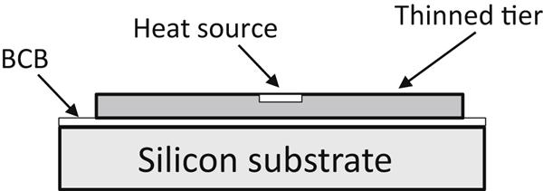
The use of both vertical and horizontal interconnections to move heat within a stacked system has been considered in systems-in-package (SiP) technologies [531]. Communication among tiers in SiP passes through vertical off-chip wires connected with wide metal stripes to the I/O pad area of each tier. An example of this technology is illustrated in Fig. 13.11. Prototype structures of this ultra-thin tier technology demonstrate several issues and tradeoffs related to thermal management of vertically integrated systems. Benzocyclobutene (BCB), for example, can be used as an adhesive layer with a thermal conductivity of 0.18 W/m-K. This material hinders the flow of heat in the vertical direction. Vertical flow of heat can be averted if the silicon substrate for each tier other than the first tier is thinned to reduce the length of the thermal path to the heat sink. This practice is beneficial; however, extreme substrate thinning in the range of 10 μm degrades thermal flow since the volume of the silicon is too small, preventing the heat from spreading laterally within the tiers, leading to hot spots [531]. Simulations have demonstrated that for the structure shown in Fig. 13.12, decreasing the BCB layer from 3 to 2 μm lowers the vertical thermal resistance of a two tier system by 22% (where the heat source area is 2×105 μm2). For the same sized heat source, the thermal resistance increases by 17% when the silicon substrate is thinned from 15 to 10 μm [531].

To further facilitate the flow of heat, an intermediate layer with embedded metal structures, such as a grid, is utilized. These structures allow the heat to spread laterally into the highly conductive vertical vias, lessening the rise in temperature. These structures, however, are only efficient for a certain physical distance from the vias, termed the effective transverse thermal transfer length,
(13.22)
where kCu and kBCB are, respectively, the thermal conductivity of copper and BCB, and tCu and tBCB are, respectively, the thickness of the copper grid/plate and BCB layer. As described in this expression, the effective thermal length does not change linearly with the transverse thermal resistance of the copper grid/plate [531].
Early investigation of thermal issues [531] demonstrated the potential and limitations of enabling faster flow of heat within 3-D systems. As fabrication processes for TSVs have evolved, the use of thermal TSVs (TTSVs) as heat conduits has gained popularity and TTSVs have been included in several physical design techniques. Alternatively, TSVs are employed as a means to shield a circuit from both rises in temperature and electrical noise generated by adjacent circuit blocks within the same tier [532]. The objective is not to facilitate the flow of heat but rather to block the rise in temperature of a circuit block from adjacent blocks dissipating significant power. The efficiency of this approach, where a metal guard ring is replaced by a ring of uniformly spaced TSVs, improves as the TSV diameter grows, as illustrated in Fig. 13.13 [532].

Although this practice is beneficial, hot spots developed within the block cannot be completely removed. This situation is more pronounced if heat is generated from the adjacent blocks in the vertical direction or if the effective thermal length limits efficient heat transfer to the periphery of the blocks. Consequently, integrating the TSV insertion process into the physical design process of a 3-D system can lead to more thermally robust and reliable solutions. Issues related to including TSVs within the physical design process include allocation or planning of the TTSVs, the system granularity to insert TSVs (for example, standard cell or block) whether TTSVs (and more broadly, temperature) is an objective or constraint, and the overhead of the TTSV on other design objectives such as performance, wirelength, and area. Several TSV planning techniques are discussed in the following subsection.
13.2.1 Thermal Via Planning Under Temperature Objectives
In Chapter 9, Physical Design Techniques for Three-Dimensional ICs, the available space among the cells or circuit blocks in each tier of a 3-D system is employed to allocate signal TSVs to least affect the placement of the components and the length of the interconnections. Similarly, the available space can also mitigate thermal issues by placing thermal vias within the whitespace. As thermal gradients differ across and among tiers, two different types of TTSV densities are typically computed. Vertical TTSV densities among tiers and a horizontal TTSV density for each tier are determined. Thermally driven methods for floorplanning, placement, and routing have been developed to determine these densities to achieve a broad repertoire of objectives.
The temperature or thermal gradients within a 3-D stack is interestingly treated as an objective and the TTSV density as a design constraint and vice versa, leading to different problem formulations. Another issue that arises is whether TTSV planning should be integrated with the floorplanning or placement steps or be applied as a postprocessing step. Integrating TTSV planning within a physical design process rather than as a postprocessing step can lead to better results, but the need for thermal analysis during each iteration can adversely affect computational time.
Extending floorplanning methods to 3-D systems, as discussed in Chapter 9, Physical Design Techniques for Three-Dimensional ICs, requires adapting the objective cost function to consider the allocation of the TTSVs. An additional term is added to the cost functions, such as in (9.9), to include the thermal objective. This added function is typically either the maximum temperature within the substrate [533] or the normalized maximum temperature with respect to the original peak temperature of the circuit [534]. Extending the cost function can, however, adversely affect both the solution time to produce a floorplan that satisfies a fixed outline and any temperature constraints [534]. To mitigate this issue, a two phase SA algorithm is applied. In this process, the SA algorithm proceeds without initially considering the thermal objective, producing a floorplan that satisfies a target outline while optimizing the wirelength and area. In the second phase, the SA algorithm includes the temperature objective. Furthermore, the SA algorithm also commences not with the lowest cost floorplan from the first phase, but rather with a higher cost floorplan to provide greater flexibility when the temperature objective is included. Both intertier and intratier moves are applied to the circuit blocks, where the sequence pair method represents the position of the blocks. A sequence pair is produced for each tier within a 3-D system. A change in the sequence pair captures a move of a block or a swap between two blocks.
TTSV assignment takes place during the second phase of the SA, where the blocks are moved to ensure that sufficient whitespace exists to accommodate any TTSV requirements. This task is driven by two guidelines, where the whitespace of the adjacent tiers overlap to allocate the TTSVs. Furthermore, the algorithm ensures greater whitespace around those blocks with higher temperatures since these blocks demand larger TTSV densities. In [534], to save computational time, TTSV assignment is typically applied during the last several iterations of the second phase. Variants of this technique, for example, single versus two phase SA based floorplanning and simultaneous versus postprocess TTSV assignment, are applied to standard benchmark circuits implemented as four tier stacks. Results on wirelength, maximum temperature, and success rates are reported in Table 13.9. The success rate indicates the percentage of valid floorplans that satisfy the fixed outline constraint out of the total number of runs. In Table 13.9, A.R. notates the aspect ratio of the outline of the floorplan, and WS denotes the area of the whitespace as a per cent of the total floorplan area.
Table 13.9
Reduction in Temperature for Thermal Driven Floorplanning With TTSV Allocation [534]
| Circuit | A.R. | WS | No TSV Assignment | TSV Assignment During SA | TSV Assignment as Postprocessing | ||||||
| Succ. Rate | HPWL | Max. Temp. | Succ. Rate | HPWL | Max. Temp. | Succ. Rate | HPWL | Max. Temp. | |||
| n100 | 1 | 10 | 100 | 201,252 | 286.337 | 100 | 203,408 | 227.840 | 100 | 202,448 | 266.073 |
| n100 | 1.5 | 10 | 100 | 201,928 | 287.679 | 100 | 206,102 | 259.817 | 100 | 203,505 | 268.282 |
| n100 | 2 | 10 | 90 | 207,032 | 284.848 | 100 | 207,750 | 241.208 | 90 | 208,537 | 257.537 |
| n100 | 2 | 15 | 100 | 207,838 | 241.368 | 100 | 211,837 | 196.453 | 100 | 209,839 | 222.829 |
| n200 | 1 | 10 | 100 | 368,415 | 311.592 | 100 | 380,961 | 271.824 | 100 | 370,457 | 289.217 |
| n200 | 1.5 | 10 | 100 | 376,818 | 292.612 | 100 | 380,787 | 249.314 | 100 | 378,891 | 266.282 |
| n200 | 2 | 15 | 90 | 387,580 | 312.756 | 90 | 389,621 | 278.527 | 90 | 391,264 | 273.262 |
| Avg. | – | – | – | 1.0× | 1.0× | – | 1.015× | 0.85× | – | 1.007× | 0.92× |
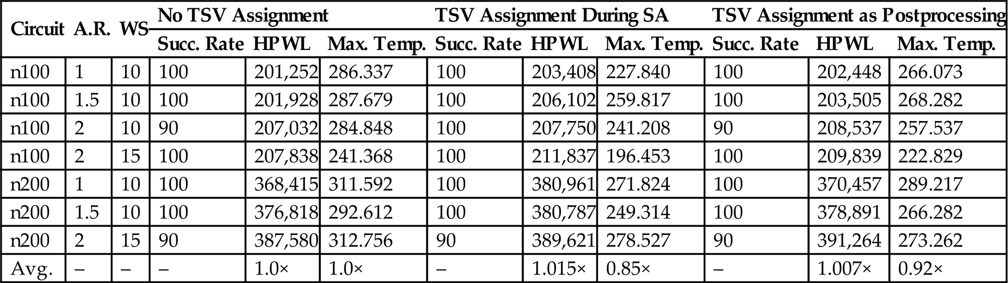
The results listed in Table 13.9 demonstrate that the maximum temperature of a 3-D circuit is reduced when TTSVs are inserted. A greater decrease in temperature is observed when TTSV planning is an integral part of the floorplanning process. Although the 3-D stacks exhibit a higher temperature than a 2-D version of the circuits, the TTSVs offer a non-negligible decrease in temperature. The computational time of the thermal aware floorplanning method including TSV planning increases by three times as compared to the case where TTSV planning is not considered.
To mitigate the increased computational times, a thermal analysis of the circuit can be performed less frequently or, alternatively, faster (yet reasonably accurate) techniques can be used rather than solving the temperature matrix in (12.44). Unlike the matrix manipulation methods in [533], thermal analysis of 3-D circuits uses random walks [535]. Moreover, the TSV planning in [533] assumes a non-fixed outline. Relaxing the outline constraint allows for a less complex objective function. A weighted term for the maximum temperature is also utilized. Having as inputs (1) a set of circuit blocks, (2) the dimensions of these blocks along with the related power consumption, (3) a connectivity netlist for the circuits blocks, and (4) certain parameters of the 3-D system, for example, the number of tiers and traits of the TTSVs, allows SA algorithms to be employed to optimize a cost function.
This function includes a weighted linear combination of wirelength and area in addition to temperature, similar to (13.1). Thus, SA progresses in a single phase but with faster thermal analysis to counterbalance the longer time needed to produce a high quality floorplan. As the TTSVs are allocated close to the high temperature blocks, the area of these blocks is enlarged to include the TTSVs, incurring an increase in area. To capture the area overhead of the TTSVs, a thermal via map is used where each entry describes the density of the TTSVs for a region of a tier. For each of these regions, space is created by vertically shifting overlapping blocks to fit the TTSVs in all of the tiers of the system, where a maximum TSV density υmax is permitted.
At every iteration of the technique, a new TTSV density is determined, described by the thermal conductivity of those regions with inserted TSVs. The updated thermal conductivity knew is
(13.23)
where kold is the existing thermal conductivity (i.e., TTSV density), and Tcur and Ttarget are, respectively, the current and target temperature of a block. The thermal conductivities are updated in descending temperatures of the blocks as the low temperature blocks require a lower TTSV density. This density for each entry of the TTSV matrix is
(13.24)
where kvia is the thermal conductivity of a single TTSV and c is a user defined constant.
The tradeoff of treating TSV planning as either an integral part of floorplanning or as a postprocessing step can again be used for runtime savings. In [534], the results are of lower quality if TTSV planning is a postprocessing step. Moreover, the use of random walks for thermal analysis allows the temperatures to be computed locally where the TTSVs are allocated to improve a hot spot. Limiting thermal analysis to a smaller area further saves computational time.
A comparison among the different approaches for TTSV planning applied to the GRSC benchmarks is listed in Table 13.10. Interestingly, if a floorplan targeting only wirelength and area is utilized as the baseline, and TTSVs are added, the resulting temperatures may be higher for certain circuits as compared to the case where a thermal driven floorplan without TTSVs is generated using the methods discussed in Section 13.1.1. This situation must not lead to the conclusion that TTSVs do not offer any benefit. Rather, omission of the temperature term in the objective function leads to highly compact floorplans that include overlaps of high temperature blocks from adjacent tiers. Adding TTSVs can cause certain blocks to shift to make space for the TTSVs. These new positions, however, may cause new overlaps that can yield higher temperatures. Instead, thermal aware floorplanning without TTSVs alleviates high temperatures by shifting blocks from each other, avoiding the creation of these hot spots. Summarizing, TTSV planning with floorplanning results in the lowest temperatures, similar to [534], yet with a non-negligible increase in area and wirelength that can reach, respectively, 47% and 22%.
Table 13.10
Comparison of Thermal Aware Floorplanning Approaches [533]
| Benchmarks | Area/Wirelength Driven | Area/Wirelength Driven With TTSVs | Thermal Driven W/O TTSVs | Integrated Approach With TTSVs | ||||||||
| Area | Wirelength | Temp. | Area | Wirelength | Temp. | Area | Wirelength | Temp. | Area | Wirelength | Temp. | |
| n50 | 58,491 | 91,521 | 136.6 | 59,309 | 91,986 | 126.5 | 62,517 | 91,363 | 120.7 | 86,093 | 102,425 | 94.1 |
| n50b | 66,490 | 87,838 | 145.1 | 72,564 | 90,886 | 115.7 | 68,694 | 85,173 | 118.1 | 82,925 | 94,088 | 108.6 |
| n50c | 63,666 | 92,418 | 129.2 | 64,521 | 92,900 | 122.1 | 64,532 | 91,808 | 110.6 | 80,303 | 100,013 | 86.8 |
| n100 | 57,664 | 135,970 | 123.6 | 61,431 | 138,729 | 92.3 | 68,480 | 142,521 | 82.0 | 83,311 | 155,972 | 87.7 |
| n100b | 49,950 | 120,431 | 112.9 | 51,095 | 121,297 | 98.0 | 61,490 | 127,801 | 84.8 | 81,893 | 148,806 | 71.7 |
| n100c | 53,040 | 132,142 | 128.8 | 54,135 | 133,800 | 95.4 | 63,745 | 138,324 | 85.7 | 81,596 | 152,045 | 76.4 |
| n200 | 50,190 | 215,549 | 135.6 | 52,472 | 218,601 | 105.2 | 62,220 | 270,123 | 97.9 | 74,414 | 310,017 | 75.8 |
| n200b | 55,385 | 226,447 | 125.9 | 57,579 | 228,792 | 103.7 | 70,596 | 250,672 | 69.1 | 82,599 | 284,590 | 98.7 |
| n200c | 52,877 | 250,970 | 123.6 | 53,601 | 251,855 | 110.8 | 66,150 | 250,582 | 74.4 | 77,465 | 304,035 | 68.7 |
| n300 | 81,340 | 313,680 | 186.9 | 83,801 | 316,041 | 146.9 | 117,600 | 334,304 | 51.4 | 136,907 | 468,086 | 56.4 |
| Avg. ratio | 1.000 | 1.000 | 1.000 | 1.035 | 1.012 | 0.831 | 1.195 | 1.054 | 0.678 | 1.473 | 1.220 | 0.625 |

This significant increase can be attributed to the large number of TTSVs at the periphery of those blocks with a high temperature. This number is large if the area of these blocks is significant, prohibiting the allocation of TTSVs close to the hot spot. Thus, thermal driven placement where the TTSVs are allocated as standard cells may be more beneficial, offering greater opportunity to reduce temperature. Contrary to temperature unaware methods for TSV planning, where inserting TSVs at the standard cell level incurs unacceptable overhead, this approach may be viable when thermal issues are considered during the design process.
Allocating TTSVs at the standard cell level decreases the physical distance between a low resistivity thermal path (i.e., the TTSV) and the heat sources (i.e., the standard cells), offering an efficient method to move heat towards the ambient. TTSV insertion can satisfy a variety of design objectives (not simultaneously), such as [536]
The design objective is to identify those regions where thermal vias are most needed (the hot spots) and place thermal vias within those regions at the appropriate density. This assignment, however, is mainly restricted by two factors: the routing blockage caused by these vias and the area of the whitespace that exists within each tier. Note that although the density of the thermal vias can vary among different whitespace allocations, the thermal vias within each whitespace are uniformly distributed.
To determine the number of thermal vias for a 3-D circuit, the temperature at specific nodes within the volume of the circuit needs to be evaluated. The finite element method combined with (13.10) and (13.11) is utilized to determine the temperature of the nodes within a 3-D grid in [536], although other methods discussed in the previous chapter can also be used. An iterative approach is applied to determine the thermal conductivity of certain elements, similar to that shown in Fig. 12.8, to minimize the thermal objective. More specifically, when initializing the optimization procedure, an ideal thermal gradient is selected when a moderate number of TTSVs are assumed. Additionally, the initial temperature profile characterizes the thermal gradients within the whitespace regions where thermal vias can be added. Furthermore, the minimum thermal conductivity is assumed for these regions, coinciding with no thermal vias in these whitespace regions. The thermal conductivity of the whitespace is iteratively modified, updating the temperature of the nodes. The algorithm terminates when any further change in the thermal conductivity does not significantly improve the desired objective.
Inserting thermal vias can significantly affect the thermal conductivity of the tiers. Since these vias facilitate the transfer of heat in the z-direction, the thermal conductivity in the z-direction significantly differs from the conductivity in the x and y directions. To quantify the effects of the thermal vias in terms of a change in the thermal conductivity within a 3-D grid, the following expressions describe the change in (13.11),
(13.25)
(13.26)
 (13.26)
dth is the density of the thermal vias and ![]() and
and ![]() are the thermal conductivity of a physical tier of a 3-D system in, respectively, the horizontal and vertical directions when no thermal vias are employed. Values of 2.15 and 1.11 W/m-K are used for, respectively [536], Ktierlateral and KtierZ for the MIT Lincoln Laboratories 3-D process technology [307]. The thermal conductivity of the vias is denoted as Kvia. The thermal conductivity of copper is 398 W/m-K. With these expressions, the vertical and lateral thermal conductivity or, alternatively, the density of the thermal vias in each region is iteratively determined until the target thermal gradient or temperature is reached. Note that (13.25) is identical to (12.12).
are the thermal conductivity of a physical tier of a 3-D system in, respectively, the horizontal and vertical directions when no thermal vias are employed. Values of 2.15 and 1.11 W/m-K are used for, respectively [536], Ktierlateral and KtierZ for the MIT Lincoln Laboratories 3-D process technology [307]. The thermal conductivity of the vias is denoted as Kvia. The thermal conductivity of copper is 398 W/m-K. With these expressions, the vertical and lateral thermal conductivity or, alternatively, the density of the thermal vias in each region is iteratively determined until the target thermal gradient or temperature is reached. Note that (13.25) is identical to (12.12).
In Fig. 13.14, (13.25) and (13.26) are plotted for a variable density of thermal vias. The thermal conductivity in the z-direction is about two orders of magnitude greater than in the horizontal direction. Only the vertical thermal conductivity is, therefore, updated during the optimization process, while the thermal conductivity in the horizontal directions are determined from the thermal via density obtained from the algorithm and (13.26).
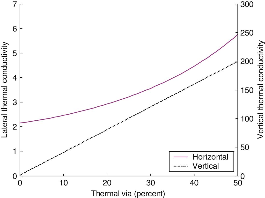
This method has been evaluated on MCNC and IBM-PLACE benchmark circuits [396], where interconnect power consumption is not considered. Some results are listed in Table 13.11. Note that the target objectives are decreased by increasing the density of the thermal vias. A considerable reduction in all of the aforementioned objectives (see, p. 491) is observed. In addition, as compared to a uniform distribution of thermal vias, fewer thermal vias are inserted to reduce the temperature. Furthermore, by analyzing the distribution of the thermal vias throughout a four tier 3-D circuit, the density of the vias is smaller in the upper tiers. This behavior is explained by noting that in a 3-D IC the thermal gradients substantially increase the temperature in the upper tiers. By placing additional thermal vias in the lower tiers, these thermal gradients are mitigated, reducing the temperature in the upper tiers.
Table 13.11
Average Per cent Change of Thermal Objectives as Compared to the Case With no Thermal Vias [536]
| Objective | Average Percent Change | |||||
| gmax | gave | Tmax | Tave | dthmax | dthave | |
| gmax | −68.1 | −60.8 | −44.5 | −25.9 | 44.9 | 10.2 |
| gave | −75.7 | −70.7 | −51.6 | −29.5 | 50 | 17.6 |
| Tmax | −71.1 | −64.5 | −47.3 | −27.3 | 50 | 12.3 |
| Tave | −73.2 | −67.4 | −49.2 | −28.3 | 50 | 14.3 |
| dthmax | −55.5 | −43.3 | −31.4 | −19.2 | 25 | 4.2 |
| dthave | −79.2 | −75.3 | −54.7 | −31.0 | 50 | 23.9 |
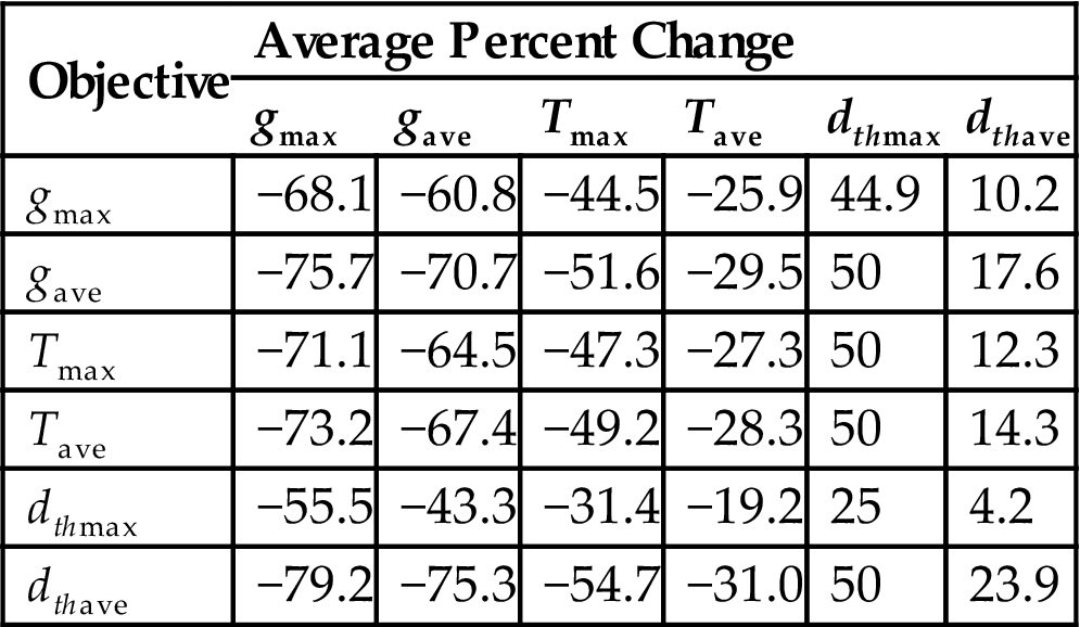
13.2.2 Thermal Via Planning Under Temperature Constraints
Although TTSVs incur area and wirelength overhead during both the floorplan and placement steps, the density constraints for TTSVs are typically not highly restrictive. The situation is more delicate if TTSV planning is applied to a later step of the design process (e.g., routing) where there is less flexibility in moving circuits blocks within the 3-D stack. In these cases, a reasonable approach is to make the TTSV density an objective where temperature is a constraint. This approach is orthogonal to the techniques presented in the previous subsection. Consequently, thermal via planning can be described as the problem of minimizing the number of thermal vias while constraining the temperature and capacity of the thermal vias. Based on these observations, the problem of determining the minimum number of TSVs to satisfy a specific temperature constraint can be described by the nonlinear programing (NLP) problem,
(13.27)
 (13.27)
where dthi is the TTSV density per tier for a 3-D circuit comprising n physical tiers. In addition, a number of constraints apply to (13.27), such as temperature (i.e., the temperature of the circuits cannot exceed a specified value), capacity of the TSVs in each tile, a lower bound on the number of TSVs to ensure that the wirelength of the circuit does not increase, and the heat flow equality (i.e., the incoming and outgoing heat flow for every tile should be equal).
Compact thermal models, such as the model described in Section 12.3, are preferred due to the lower computational time required to obtain the thermal profile of 3-D circuits as compared to finite element and finite difference methods [351,537–539]. Using the compact thermal model as a baseline, described in Section 12.3, a 3-D circuit is discretized into tiles. The tiles located at the same x–y coordinates but on different tiers constitute a pillar modeled by a group of serially connected resistors and heat sources (see Fig. 12.9).
Relating the thermal conductivity of the TSVs with the serially connected resistors in a single pillar, (13.27) can be rewritten as
(13.28)
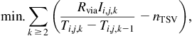 (13.28)
where Rvia is the thermal resistance of one TSV [465] and nTSV is the number of TSVs that exhibit the same thermal resistance as a tile within a 3-D grid. Ii,j,k and Ti,j,k are, respectively, the heat flow in the z-direction and temperature of the tiles in the grid, and i, j, and k are the indices of the tiles.
Efficiently solving this NLP is a formidable task. The thermal via planning process is, therefore, divided into a two stage problem: determining the intratier TTSV density within each tier of a 3-D circuit and determining the intertier TTSV density among the tiers within the stack. Depending upon the formulation of these problems and the applied constraints, different intratier and intertier distributions of TTSVs are produced.
13.2.3 Multi-level Routing
The technique of multi-level routing [539,540] is extended to 3-D ICs including thermal via planning. Multi-level routing with thermal via planning can be treated as a three stage process, illustrated in Fig. 13.15, which includes a coarsening phase, initial solution generation at the coarsest level of the grid, and subsequent refinement process until the finest level of the grid is reached. Before the coarsening phase is initiated, the routing resources, capacity of the TSVs, and power density in each tile are determined. The power density and routing resources are determined during each coarsening step. At the coarsest level (level k), an initial routing tree is generated. At this point, the TSV planning step is invoked, assigning TSVs to each tile within a coarse grid. During the refinement phase, the TSVs are distributed to preserve the solution produced during the previous level. If the final temperature at the end of the refinement phase does not satisfy a specified temperature, the TSVs are further adjusted to achieve the target temperature.

The TSV planning step is based on the alternating direction TSV planning (ADVP) algorithm, which distributes the TSVs in alternate directions. The TSVs are distributed during the first step among the tiers of the 3-D IC and, during the second step, within each tier of the circuit. This algorithm reduces overall runtime since the thermal profile during the multi-level routing process increases the execution time. The problem of distributing the TSVs among the tiers of a 3-D system can be described as a convex problem. An analytic solution is determined if the capacity bounds for the TSVs are removed,
(13.29)
 (13.29)
where ai and ![]() are, respectively, the number of TSVs and the power density of each tile of a grid consisting of n tiers.
are, respectively, the number of TSVs and the power density of each tile of a grid consisting of n tiers.
A corresponding analytic solution cannot be easily determined, however, for the horizontal or intratier distribution of TSVs. Alternatively, heat propagation and path counting replace the thermal profiling step. Heat propagation considers the propagation of the heat flow among the tiles of the grid and is determined by evaluating the different paths for transferring heat to the lower tiers of the grid. Different heat propagation paths are illustrated in Fig. 13.16.
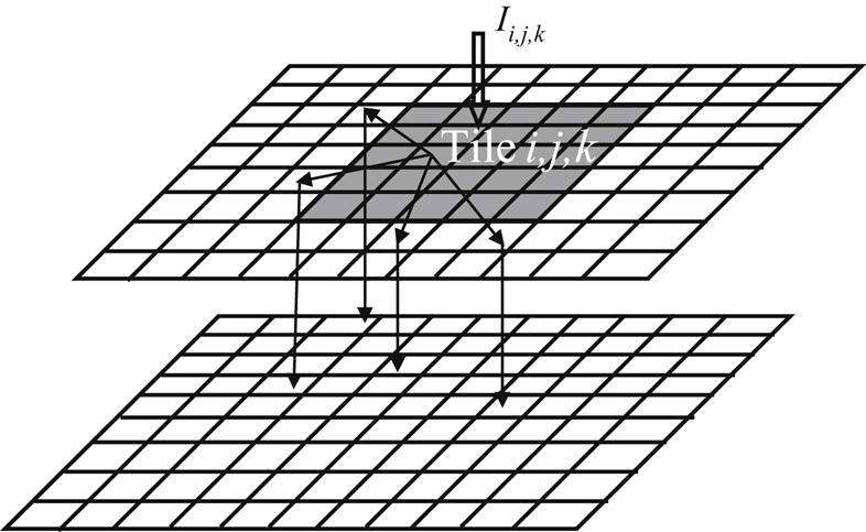
The multi-level routing and ADVP algorithm are applied to MCNC benchmarks and compared to both the TSV planning approach described in [537] and to a uniform distribution of TSVs. As listed in Table 13.12, the ADVP algorithm achieves a significant decrease in the number of TSVs to maintain the same temperature, likely resulting in lower fabrication cost and less routing congestion. From Table 13.12, a considerable reduction in the number of TSVs is achieved by the ADVP algorithm without an increase in computational time.
Table 13.12
Comparison of TSV Planning Techniques
| Circuits | m-ADVP [538] | m-VPPT [537] | Uniform TSV | |||||||||
| T (°C) | #TSV | Area Ratio | Runtime (s) | T (°C) | #TSV | Area Ratio | Runtime (s) | T (°C) | #TSV | Area Ratio | Runtime (s) | |
| ami33 | 77.0 | 1282 | 2.5% | 1.55 | 77.1 | 1801 | 3.5% | 1.76 | 77.1 | 2315 | 4.5% | 1.62 |
| ami49 | 77.0 | 20,956 | 0.9% | 13.5 | 77.1 | 43,794 | 1.8% | 12.15 | 76.9 | 166,366 | 6.8% | 16.17 |
| n100 | 77.0 | 11,885 | 1.5% | 7.66 | 77.0 | 22,211 | 2.8% | 8.31 | 76.8 | 30,853 | 3.9% | 7.54 |
| n200 | 77.0 | 13,980 | 1.8% | 12.24 | 77.2 | 18,835 | 2.4% | 10.89 | 77.1 | 30,346 | 3.9% | 12.21 |
| n300 | 77.0 | 17,646 | 1.3% | 20.44 | 77.1 | 30,161 | 2.2% | 21.73 | 76.9 | 57,342 | 4.2% | 22.42 |
| Avg. | 1.0 | 1.6% | 1.0 | 1.68 | 2.6% | 1.01 | 3.55 | 4.6% | 1.06 | |||
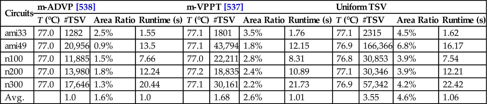
Although the ADVP algorithm reduces the number of TTSVs, a further decrease in the TTSV density is achieved by applying a different approach to determining the local TSV densities. Both the intertier and intratier via density problem are converted into a convex problem through several simplifications [541]. The primary assumption of this approach is that the silicon substrate of each of the upper physical tiers and the bonding material at the interface between two tiers are treated as a single material with homogeneous material properties. The thickness of this material is the summation of the thickness of the silicon layer and the bonding layer, with a thermal conductivity Kavg equal to the average thermal conductivity of the silicon and bonding material. The solution of these convex problems produces a different distribution of intertier and intratier TSVs [541], as compared to the distribution produced by ADVP and a uniform TSV distribution. These differences are summarized in Table 13.13, where Kvia is the thermal conductivity of the TSVs, and S is the area of the circuit blocks within each tier of a 3-D system.
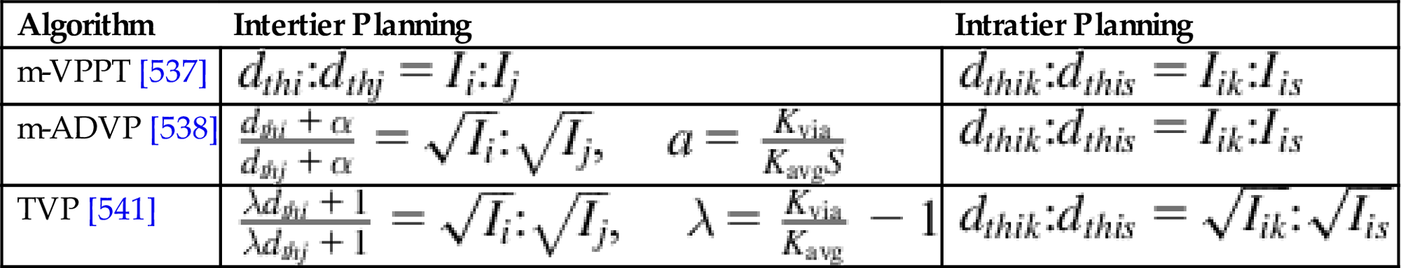
This modified thermal via planning step has been applied to MCNC and GSRC benchmark circuits and compared with the ADVP and other TSV distribution algorithms [537,538]. Some results are reported in Table 13.14, where the solution of the approximate convex problems reduces the number of thermal vias required to reach a prespecified temperature.
Table 13.14
Comparison Among the Required Numbers of TSVs
| Circuit | m-ADVP [538] | m-VPPT [537] | TVP [541] | |||
| Tmax | #T-via | Tmax | #T-via | Tmax | #T-via | |
| ami33 | 76.8 | 1109 | 76.7 | 1360 | 77.5 | 981 |
| ami49 | 77.0 | 21,668 | 77.1 | 28,793 | 77.2 | 19,857 |
| n100 | 77.2 | 16,731 | 76.9 | 25,205 | 77.0 | 14,236 |
| n200 | 77.1 | 14,273 | 76.4 | 17,552 | 77.1 | 12,566 |
| n300 | 76.8 | 19,337 | 76.5 | 25,995 | 76.9 | 17,853 |
| Avg. | 1.12 | 1.51 | 1.00 | |||
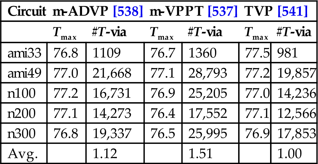
The improved thermal via planning step is integrated into a hierarchical floorplanning technique [541] for 3-D circuits, where the circuit blocks are initially partitioned onto the tiers of the circuit. Since no intertier moves are allowed after the partitioning step is completed, the partitioning step is crucial in determining the overall quality of the final result. This partitioning problem is treated as a sequence of knapsack problems [542], where the hottest blocks are placed on the lower tiers of a 3-D circuit to prevent steep thermal gradients. The heat generated by these blocks is transferred to the heat sink. Furthermore, overlap among these high power density blocks is avoided. The integrated thermal via planning and floorplanning approach is compared with a non-integrated approach, where the floorplan (initially omitting the thermal objectives) is generated first, followed by thermal via planning during a postprocessing step. The integrated technique requires 16% fewer thermal vias to achieve the same temperature, with a 21% increase in computational time and an almost 3% reduction in total area.
Note that in these techniques the dependence between temperature and power is not considered, which produces a pessimistic result with higher TTSVs densities. This pessimism is due to the reduction in leakage power as the initial temperature is decreased towards the target low (or minimum) temperature. Thus, linking the power of the circuit with the decrease in temperature gained by the TTSVs can produce a target temperature with fewer TTSVs that, in turn, lowers the area and wirelength overhead while more easily satisfying the performance objectives [543].
13.2.4 Thermal Wire Insertion
In addition to the benefits of the added thermal vias, thermal wires can enhance the heat transfer process. These thermal wires are horizontal wires that connect regions with different thermal via densities through TTSVs. These thermal wires are treated as routing channels wherever there are available tracks. Both TTSVs and wires can be integrated into the routing process [544]. Given a placement of cells within a 3-D IC, the technology parameters, and a temperature constraint, sensitivity analysis and linear programming methods are utilized to route a circuit. For routing purposes, a 3-D grid is imposed on a 3-D circuit, as shown in Fig. 13.17 for a two tier 3-D circuit. The thermal model of the circuit is based on a resistive network, as discussed in Section 12.3. Note that interconnect power is not considered in this thermal model [544].

Placing TTSVs and wires to decrease the circuit temperature adversely affects the available routing resources while increasing the routing congestion. Each vertical edge of the routing grid is, therefore, associated with a specific capacity of intertier vias. A similar constraint applies for the horizontal edges, which represent horizontal routing channels. The width of the routing channel is equal to the edge width of the tiles. As shown in Fig. 13.18, the thermal wire and vias affect the routing capacity of each tile.
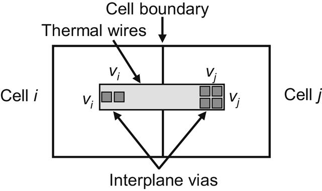
The 3-D global routing flow is depicted in Fig. 13.19, where thermal vias and wires are inserted to achieve a target temperature under congestion and capacity constraints. A 3-D minimum Steiner tree is initially generated, followed by an intertier via assignment. A 2-D maze router produces a thermally driven route within each tier of the circuit. In the following steps [544], an iterative procedure is applied to insert the thermal vias and wires and complete the physical routing process. A sensitivity analysis is used to perform a linear programing based thermal via and wire insertion process during the first step of the iterative procedure. If an insertion violates any congestion constraints or causes overflow in the routing channels, a rip-up and route step is used to resolve these conflicts [544]. The thermal profile and sensitivity analysis steps are repeated to determine whether the target temperature has been achieved. The iterations are terminated when no remaining violations exist or the temperature of the circuit cannot be improved. The complexity of the algorithm is bounded by the complexity of the iterative procedure. The complexity of each iteration is O(NGlogG+G3) where N and G are, respectively, the number of nets in the circuit and the number of cells in the routing grid.

To determine the efficiency and overhead of inserting thermal wires, a number of benchmark circuits have been routed with several routing approaches that employ different thermal management methods. The traits of the benchmark circuits are listed in Table 13.15 and are based on the MCNC and IBM placement benchmark suites [506]. All of the benchmark circuits are composed of a small number of circuit blocks, and the largest routing grid includes 1,600 unit grid cells.
Table 13.15
Benchmark Circuits and Routing Grid Size [544]
| Circuit | # of Circuit Blocks | # of Nets | Grid Size |
| biomed | 6417 | 5743 | 28×28 |
| industry2 | 12,149 | 12,696 | 31×31 |
| industry3 | 15,059 | 21,939 | 35×35 |
| ibm06 | 32,185 | 33,521 | 40×40 |
The thermal via and wire insertion process integrated with the routing process (TA) is compared to routing with thermal via and wire insertion as a postprocessing step after global routing (P), and simultaneous routing and thermal via insertion but without the use of thermal wires (V). Some results describing the peak temperature, wirelength, and computational time based on these methods are reported in Table 13.16. Note the excessively high temperatures when no thermal management is employed. This situation is due to the assumption of 0°C as the ambient temperature in [544], while the target maximum temperature is 80°C. As shown by these results, inserting auxiliary wires is another means to further lower temperature within a 3-D system with a small increase in wirelength.
Table 13.16
Comparison of Various Metrics Among Different 3-D Global Routing Approaches [544]
| Circuit | Tinit (°C) | Peak Temperature | Wirelength (×105) | Computational Time (s) | ||||||
| TA | P | V | TA | P | V | TA | P | V | ||
| biomed | 237.1 | 81.9 | 105.6 | 115.3 | 1.82 | 1.77 | 1.78 | 255 | 137 | 188 |
| industry2 | 207.5 | 82.4 | 106.6 | 116.3 | 6.04 | 5.92 | 6.01 | 855 | 473 | 591 |
| industry3 | 202.0 | 79.2 | 99.1 | 112.5 | 9.85 | 9.75 | 9.71 | 1807 | 1405 | 1686 |
| ibm06 | 236.4 | 81.2 | 99.2 | 131.4 | 18.08 | 18.19 | 18.12 | 2956 | 1585 | 2274 |

13.3 Hybrid Methodologies for Thermal Management
Methods that either redistribute the power densities within a 3-D system (either dynamically or during design time) or increase the thermal conductivity of the tier, allowing heat to be removed faster, are presented in the previous two sections. Cooling methods, however, are not considered. More complete thermal management solutions based on external cooling strategies are the focus of this section. These techniques consider the features of the cooling mechanism and combine thermal management both at runtime and during design time as an efficient manner to control thermal issues. Methods to best combine liquid cooling with dynamic thermal management and thermal aware design to satisfy temperature constraints while limiting the effects of high temperatures on system reliability are discussed in this section.
Liquid cooling systems and microchannels etched in the substrate between tiers are discussed in Chapter 12, Thermal Modeling and Analysis. Those parameters affect the heat removal capacity of liquid cooling, including the type of coolant, flow rate of the fluid, and energy dissipated by the cooling mechanism. Combining this mechanism with dynamic thermal management, for example, task migration, task scheduling, and DVFS, results in a large solution space that can be further increased if thermal aware floorplanning is added as another thermal management option. All of these methods make thermal optimization challenging.
Another important aspect of hybrid thermal management is the response time to address thermal events (i.e., exceeding a temperature or thermal gradient threshold). Liquid cooling includes mechanical parts and, therefore, changes in the cooling system, for example, the flow rate, require a relatively long time as compared to the thermal constant of the system and the response time of other dynamic thermal management techniques. To illustrate the interplay among the different thermal management approaches, a 3-D MPSoC is discussed where liquid cooling, workload scheduling, DVFS, and thermal aware floorplanning are employed to address the peak temperature and thermal gradients.
Two and four tier MPSoCs are considered where, respectively, one and two tiers include an UltaSPARC T1 processor [545] consisting of eight cores and caches. The other tiers contain the L2 cache and part of the crossbar switch connecting the cores and caches within the MPSoC. A floorplan of the tiers are depicted in Fig. 13.20A. A 90 nm CMOS node is assumed as the manufacturing technology for these 3-D systems. Cavities are etched into the substrate of each tier, forming microchannels with a cross-section of 100 μm × 100 μm and a pitch of 100 μm. Intertier interconnects with a uniform distribution of TSVs, a TSV diameter of 50 μm, and a TSV pitch of 100 μm are assumed. A uniform distribution of TSVs is a restrictive assumption, where a nonuniform distribution of TSVs is more common and has a lower impact on wirelength. Based on these traits and the area of the tiers within the MPSoC, 66 microchannels are used within each tier [546]. Furthermore, convective single phase cooling is assumed, where the coolant is water and the cooling system is supplied by a pump and regulated by valves. The flow rate within the microchannels ranges from 0.01 to 0.0323 L/min. A single pump supplies 60 3-D MPSoCs, and the power can reach 180 watts, demonstrating that the energy requirements of the cooling system are not negligible. Exploiting other less power demanding techniques can be combined with liquid cooling to lower the power budget of the cooling mechanism in addition to the power consumed by the MPSoC [546].

Liquid cooling removes heat faster from those cores located close to the inlet port since the temperature of the coolant is lower at this point, allowing more heat to be removed. As the temperature of the coolant increases towards the outlet port at a fixed rate along the flow direction (i.e., the flow is thermally developed), less heat is removed and, therefore, those cores located close to the outlet port exhibit higher temperatures. Varying the flow rate within the microchannels improves the heat removal properties, although a similar thermal behavior across the tier is observed. The higher flow rate allows more heat flux to be absorbed as the fluid more quickly exits the microchannels, leading to lower temperatures at the outlet port of the microchannel. The difference in temperature of the cores for different flow rates is significant and can reach 40°C for those cores located close to the outlet port. Alternatively, this temperature variation is much lower for the cores located at the inlet port of the microchannels. The temperature of the fluid is low at the inlet port and does not significantly vary with the flow rate, exhibiting similar heat removal capabilities over the range of flow rates.
High flow rates can decrease the core temperature below typical operating conditions while simultaneously dissipating high power. This observation has motivated the introduction of other less power demanding (and faster) methods to lower the temperature within 3-D MPSoCs. In addition, liquid cooling is susceptible to spatial thermal gradients due to the thermal development of the fluid in the microchannel. Task scheduling and migration are, therefore, combined with liquid cooling since the temperature of those cores closer to the inlet port exhibit a lower temperature. Employing different utilization rates, e.g., 90%, 70%, 40%, and 10%, each core is assigned a utilization ratio to satisfy the temperature limits [546]. Among the different core workloads, the smallest difference in temperature among the cores is observed when a “flow descending” allocation of tasks is performed. This allocation implies that higher utilization rates are assigned to those cores close to the inlet port of the fluid. This assignment avoids the creation of hot spots while also reducing thermal gradients across the tiers. To consider thermal gradients due to liquid cooling, the task utilization method employs a queue of tasks adjusted to include the position of the cores with respect to the distance of the cores from the inlet ports of the microchannel [546].
DVFS is also explored as another DTM method to address thermal issues. Two different voltage/frequency pairs are assumed, the nominal (V, F) of (0.91 V, 0.84 F) and (0.83 V, 0.67 F). The cores switch between voltage/frequency pairs for different temperature ranges, where a core temperature below the lower bound leads to an increase in frequency, while a slower voltage/frequency pair is selected if the upper bound is exceeded. The temperature ranges are (73, 77) °C, (78, 80) °C, and (82, 85) °C. The application of DVFS is affected by the thermal gradients caused by the liquid cooling. Thus, those cores located closer to the outlet port switch more frequently between voltage/frequency pairs as compared to the cores close to the inlet port.
These results demonstrate that the different thermal management techniques are interdependent and should not be applied separately. Since each of the techniques is characterized by a different overhead type and magnitude, each technique is applied only as long as required.
A complex system is often controlled by both cyber physical [547] and rule-based fuzzy controllers [546]. A set of rules are listed in Table 13.7, where three factors, the distance (D) from the inlet port, temperature (T), and utilization (U) of each core, can be categorized as low (L), medium (M), and high (H). The rules indicate the fuzzy controller decisions based upon the voltage/frequency pair of each core and the flow rate. The fuzzy controller can be implemented as a software routine, which is invoked each time a thermal map of the system is obtained through thermal sensors. In [546], this sampling occurs every 100 ms. Additionally, the core utilizations are computed within the same interval based on the workload of the queue for each core. With this information and the set of rules listed in Table 13.17, the fuzzy controller selects the appropriate voltage/frequency pair for each core and the flow rate of the fluid.
Table 13.17
A Set of Rules for the Fuzzy Controller (X is a “don’t care”) [546]
| IF | THEN | |||
| D Is | AND T Is | AND U Is | V/F Is | AND Flow Rate Is |
| L | X | X | H | L |
| M | L | X | H | L |
| M | M | L | L | L |
| M | M | M | M | M |
| M | M | H | M | M |
| M | H | L | L | L |
| M | H | M | M | M |
| M | H | H | M | H |
| H | L | X | H | L |
| H | M | L | L | L |
| H | M | M | M | L |
| H | M | H | H | M |
| H | H | L | L | M |
| H | H | M | L | H |
| H | H | H | M | H |

This thermal management framework is compared with several other thermal management policies. A case where standard air cooled packaging is used for the stack is compared to the liquid cooling solution with a variable flow rate. The air cooled system leads to prohibitive temperatures for a four tier system, ranging up to 178°C. The thermal gradients, however, do not exceed 10°C across tiers for a four tier system. The peak temperatures are much lower for the liquid cooled system ranging between 56°C to 85°C for different liquid flow policies. If only liquid cooling is employed for the bottom tier, the resulting thermal gradients within the stack are higher, reaching 15°C for a two tier system. If liquid cooling is applied to each tier, however, the thermal gradients are less than 5°C for two tiers.
Consequently, liquid cooling offers higher efficiency in reducing temperatures if combined with position aware workload scheduling and DVFS. High flow rates lower the temperature, yet the power of the pump and other components of the system lessen the advantages of this approach. To avoid this situation, lower flow rates are selected to produce thermally efficient 3-D stacks. Small deviations from the target temperature can be addressed by DVFS and/or task migration. Both methods require lower overhead and shorter response time. A fuzzy controller affects the flow and utilization rates, achieving a 63% decrease in the energy of the cooling system when the maximum flow rate is used.
A last noteworthy point is that the inherent traits of liquid cooling can be considered in the design flow to further improve the thermal behavior of 3-D systems. As an example, the floorplan shown in Fig. 13.20B is used when a core is replaced with a portion of an L2 cache. This mixed floorplan reduces the heat absorbed at the outlet port of the microchannels. Placing the low power caches in these locations balances the temperature across the tiers, employing fewer thermal techniques, each of which requires a performance and/or power overhead.
13.4 Summary
Thermal management techniques for 3-D ICs both during design time and online are discussed in this chapter. The important concepts of this chapter are summarized as follows:
• Thermal management methodologies can be roughly distinguished into: (1) approaches which control the power densities within the volume of the 3-D systems, and (2) those techniques that target an increase in the thermal conductivity of a 3-D stack.
• Physical design techniques, such as floorplanning, placement, and routing, use a thermal objective to manage thermal issues in 3-D ICs. These techniques decrease thermal gradients and temperatures in 3-D circuits by redistributing the blocks among and within the tiers of a 3-D circuit.
• Thermal management during design time requires frequent thermal analysis of the 3-D stack. The time required for this task depends on the thermal model and the analysis method. More accurate thermal models achieve improved results but often require unacceptably high computational time. Alternatively, simpler models reduce runtime but are often inaccurate.
• A compromise between the accuracy and computational requirements of the thermal model is necessary.
• The heat in 3-D ICs primarily flows vertically rather than laterally. Consequently, the thermal resistance in the horizontal direction can be treated as a constant to improve the computational time for thermal profiling.
• The third dimension can greatly affect the computational time by significantly increasing the solution space of the thermal design techniques.
• A multitude of optimization methods have been employed to design a 3-D circuit with respect to temperature and thermal gradient constraints, including SA, force directed methods, genetic algorithms, and convex, linear, and non-linear programming.
• In SA based techniques, multi-phase techniques are faster if only temperature is considered during certain stages.
• Dynamic thermal management has also been applied to 3-D systems. These methods consider the strong vertical thermal coupling to adapt established techniques employed for 2-D circuits, such as task scheduling and migration, DVFS, clock throttling, and power gating.
• Multi-level dynamic thermal management operating at both global (3-D stack) and local (per core) levels offer greater flexibility to control temperature at lower overhead.
• Formal control methods can be applied but often low overhead heuristics integrated as software routines in the operating system kernel are preferred.
• Dynamic thermal management techniques assign similar operating frequencies and tasks to cores within a tier but disparate frequencies and tasks for cores in different physical tiers.
• Intertier vias that do not carry an electrical signal are called thermal or dummy vias (TTSVs). These thermal vias are utilized in 3-D circuits to transfer heat to the ambient.
• Techniques for TTSV planning should consider several issues such as the system granularity at which TSV insertion is applied—for example, standard cell or block—whether TTSVs (and more broadly temperature) is an objective or a constraint, and the overhead of the thermal TSV, such as performance, wirelength, and area.
• TTSVs create routing obstacles. These vias should, therefore, be judiciously inserted and the allocation performed within the available whitespace within the tiers.
• Thermal via planning describes the problem of either minimizing the number of thermal vias while satisfying temperature and intertier via capacity constraints or optimizing a multiobjective function including temperature under TTSV density constraint(s). Thermal via planning techniques can significantly decrease the temperature and thermal gradients within a 3-D circuit.
• Thermal wires in the horizontal direction are equivalent to thermal vias and can lower thermal gradients in 3-D circuits by facilitating the flow of heat within tiers.
• Combining active cooling with dynamic and physical design thermal management techniques offers the greatest temperature reduction in 3-D systems.
• Active (liquid) cooling can drastically decrease the temperature throughout a 3-D stack but suffers from a long response time, increased power requirements for the cooling mechanism, and spatial thermal gradients.
• Augmenting thermal management with task scheduling and/or migration alleviates some of these issues.
• DVFS supports finer temperature control, leading to superior solutions as compared to individually applying each of these techniques.
• Adapting the floorplan of a 3-D system to the features of the cooling system provides another opportunity to further regulate temperature and thermal gradients, offering a holistic thermal management methodology.