3-D Circuit Architectures
Abstract
Exploiting the advantages of 3-D integration requires the development of novel circuit architectures. A 3-D version of a microprocessor memory system is a primary example of the architectures discussed in this chapter. Major improvements in throughput, power consumption, and cache miss rate are demonstrated. Communication centric architectures, such as a network-on-chip, are also discussed. On-chip networks are an important design paradigm to appease the interconnect bottleneck, where information is communicated among circuits within packets in an Internet-like fashion. The synergy between these two design paradigms, networks-on-chip and 3-D, to significantly improve performance while decreasing the power consumed in communications limited systems is described.
Keywords
3-D microprocessor; 3-D cache memory; 3-D networks-on-chip; 3-D NoC power models; 3-D NoC performance models
Technological, physical, and thermal design methodologies have been presented in the previous chapters. The architectural implications of adding the third dimension in the integrated circuit (IC) design process are discussed in this chapter. Various wire limited integrated systems are explored where the third dimension can mitigate many interconnect issues. Primary examples of this circuit category are the microprocessor memory system, on-chip networks, and field programmable gate arrays (FPGAs). Although networks-on-chip (NoC) and FPGAs are generic communication fabrics as compared to microprocessors, the effects of the third dimension on the performance of a microprocessor are discussed here due to the importance of this circuit type.
The performance enhancements that originate from the 3-D implementation of wire dominated circuits are presented in the following sections. These results are based on analytic models and academic design tools under development with exploratory capabilities. Existing performance limitations of these circuits are summarized in the following section, where a categorization of these circuits is also provided. 3-D architectural choices and corresponding tradeoffs for microprocessors, memories, and microprocessor memory systems are discussed in Section 20.2. 3-D topologies for on-chip networks are presented and evaluated in Section 20.3. Both analytic expressions and simulation tools are utilized to explore these topologies. Finally, the extension to the third dimension of an important design solution, namely FPGAs, is analyzed in Section 20.4. A brief summary of the analysis of these 3-D architectures is offered in Section 20.4.
20.1 Classification of Wire Limited 3-D Circuits
Any 2-D IC can be vertically fabricated with one or more processes developed for 3-D circuits. The benefits, however, vary for different circuits [291]. Wire dominated circuits are good candidates for vertical integration since these circuits greatly benefit from the significant decrease in wirelength. Performance projections as previously discussed in Chapter 7, Interconnect Prediction Models, highlight this situation. Consequently, only communication centric circuits are emphasized in this discussion. The different circuit categories considered in this chapter are illustrated in Fig. 20.1.

The first category includes application specific ICs (ASIC) that are typically part of a larger computing system. A criterion for a circuit to belong to this category is whether the third dimension can considerably improve the primary performance characteristics of a circuit, such as speed, power, and area. A fast Fourier transform circuit is an example of a 3-D ASIC [705]. Memory arrays and microprocessors are other circuit examples that belong to this category. 3-D integration is amenable to the interconnect structures connecting these components comprising more complex integrated systems.
Communication fabrics, such as NoC and FPGAs, are particularly appropriate for vertical integration. For instance, several low latency and high throughput multi-dimensional topologies have been presented in the past for traditional interconnection networks, such as 3-D meshes and tori [706]. These topologies, depicted in Fig. 20.2, are not usually considered for on-chip networks due to the long interconnects that hamper the overall performance of the network. These limitations are naturally circumvented when a third degree of design freedom is added.

In the case of FPGAs, a design style for an increasing number of applications, vertical integration offers a twofold opportunity; increased interconnectivity among the logic blocks (LBs) as well as shorter distances among these blocks. These advantages will enhance the performance of FPGAs which is the major impediment of this design style. Consequently, 3-D architectures are indispensable for contemporary FPGAs. Each of these circuit categories is successively reviewed in the remainder of the chapter. Related design tools are also discussed and further issues in the design of these circuits are highlighted.
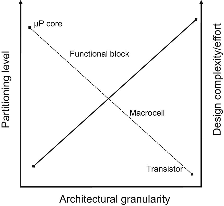
20.2 3-D Microprocessors and Memories
Microprocessor and memory circuits constitute a fundamental component of every computing system. Due to the use of these circuits in myriads of applications, the effects of 3-D integration on this system are of significant interest. Both of these types of circuits are amenable to a variety of 3-D architectural alternatives. The partitioning scheme used on standard 2-D circuits drastically affects the characteristics of the resulting 3-D architectures. The different partitioning levels and related building elements based on these partitions are illustrated, respectively in Figs. 20.3 and 20.4. A finer partitioning level typically requires a larger design effort and higher vertical interconnect densities. Consequently, each partitioning level is only compatible with a specific 3-D technology. Note that the intention here is not to determine an effective partitioning methodology specific to 3-D microprocessors and memories but rather to determine the architectural granularity that improves the performance of these circuits. The physical design techniques described in Chapter 9, Physical Design Techniques for Three-Dimensional ICs, can be used to achieve the optimum design objectives for a particular architecture.

Different architectures for several blocks not including the on-chip cache memory of a microprocessor are discussed in Section 20.2.1. The 3-D organization of the cache memory is described in Section 20.2.2. Finally, the 3-D integration of a combined microprocessor and memory is discussed in Section 20.2.3.
20.2.1 3-D Microprocessor Logic Blocks
The microprocessor circuit analyzed herein consists of one logic core and an on-chip cache memory. The architectures can be extended to multicore microprocessor systems. For a microprocessor circuit, partitioning the functional blocks or macrocells (i.e., circuits within the functional blocks) to several tiers (see Fig. 20.4) is meaningful and can improve the performance of the individual functional blocks and the microprocessor. For a microprocessor system, partitioning at the core level is also possible. The resulting effects on a microprocessor are higher speed, additional instructions per cycle (IPC), and a decrease in the number of pipeline stages.
In general, the 3-D implementation of a wire limited functional block (i.e., partitioning at the macrocell level) decreases the dissipated power and delay of the blocks. The benefits, however, are minimal for blocks that do not include relatively long wires. In this case, some performance improvement exists due to the decrease in the area of the block and, consequently, in the length of the wires traversing the block. In addition to the cache memory, many other blocks within the processor core can be usefully placed on more than one physical tier. These blocks include, for example, the instruction scheduler, arithmetic circuits, content addressable memories, and register files.
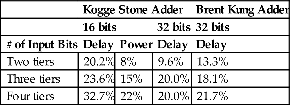
The instruction scheduler is a critical component constraining the maximum clock frequency and dissipates considerable power [707]. Placing this block in two tiers results in a lower delay and power by, respectively 44% and 16%, [708]. Additional savings in both delay and power are achieved by using three or four tiers; however, the savings saturate rapidly. This situation is more pronounced in the case of arithmetic units, such as adders and logarithmic shifters. Delay and power improvements for Brent Kung [709] and Kogge Stone [710] adders are listed in Table 20.1. As indicated from these results, the benefits of utilizing more than two tiers are negligible. Further reductions in delay are not possible for more than two tiers since the delay of the logic dominates the delay of the interconnect.
Table 20.1
Performance and Power Improvements of 3-D over 2-D Architectures [708]
| Kogge Stone Adder | Brent Kung Adder | |||
| 16 bits | 32 bits | 32 bits | ||
| # of Input Bits | Delay | Power | Delay | Delay |
| Two tiers | 20.2% | 8% | 9.6% | 13.3% |
| Three tiers | 23.6% | 15% | 20.0% | 18.1% |
| Four tiers | 32.7% | 22% | 20.0% | 21.7% |
Consequently, partitioning at the macrocell level is not necessarily helpful for every microprocessor component and should be carefully applied to ensure that only the wire dominated blocks are designed as 3-D blocks. Alternatively, another architectural approach does not split but simply stacks the functional blocks on adjacent physical tiers, decreasing the length of the wires shared by these blocks. As an example of this approach, consider the two tier 3-D design of the Intel Pentium 4 processor where 25% of the pipeline stages in the 2-D architecture are eliminated, improving performance by almost 15% [711]. The power consumption is also decreased by almost 15%. A similar architectural approach for the Alpha 21364 [712] processor resulted in a 7.3% and 10.3% increase in the IPC for, respectively two and four tiers [713].
A potential hurdle in the performance improvement is the introduction of new hotspots or an increase in the peak temperature as compared to a 2-D version of the microprocessor. Thermal analysis of the 3-D Intel Pentium 4 has shown that the maximum temperature is only 2 °C greater as compared to the 2-D counterpart, reaching a temperature of 101 °C [713]. If maintaining the same thermal profile is a primary objective, the power supply can be scaled, partially limiting the improved performance. For this specific example, voltage scaling pacified any temperature increase while providing an 8% performance improvement and 34% decrease in power (for two tiers) [711]. In these case studies, a 2-D architecture has been redesigned into a 3-D microprocessor architecture. Greater enhancements can be realized if the microprocessor is designed from scratch, initially targeting a 3-D technology as compared to simply migrating a 2-D circuit into a multi-tier stack. A considerable portion of the overall performance improvement in a microprocessor can be achieved by distributing the cache memory onto several physical tiers, as described in the following section.
20.2.2 3-D Design of Cache Memories
Data exchange between the processor logic core and the memory has traditionally been a fundamental performance bottleneck. Therefore, a small amount of memory, specifically cache memory, is integrated with the logic circuitry offering very fast data transfer, while the majority of the main memory is placed off-chip. The size and organization of the cache memory greatly depend upon the architecture of the microprocessor and has steadily increased over the past several microprocessor generations [714,715]. Due to the small size of the cache memory, a common problem is that data are often fetched from the main memory. This situation, widely known as a cache miss, is a high latency task. Increasing the cache memory size can partly lower the cache miss rate. 3-D integration supports both larger and faster cache memories. The former characteristic is achieved by adding more memory on the upper tiers of a 3-D stack, and the latter objective can be enhanced by constructing novel cache architectures with shorter interconnects.
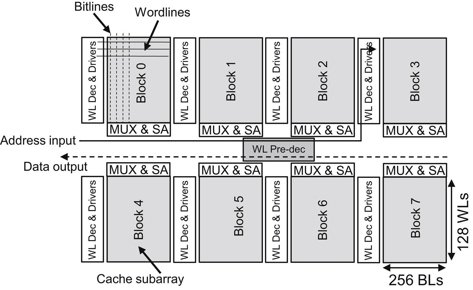
A schematic view of a 2-D 32 KB cache is illustrated in Fig. 20.5, where only the data array is depicted. The memory is arranged into smaller arrays (subarrays) to decrease both the access time and power dissipation. Each memory subarray i is denoted as Block i. The size of the subarrays is determined by two parameters, Ndwl and Ndbl, which correspond, respectively, to the divisions of the initial number of word and bit lines. In this example, each subarray contains 128×256 bits. In addition to the SRAM arrays, other circuits are shown in Fig. 20.5. The local word line decoders and drivers are placed on the left side of each subarray. The multiplexers and sense amplifiers are located on the bottom and top side of each row. The word line predecoder is placed at the center of the entire memory.
Several ways exist to partition this structure into multiple tiers. An example of a 2-D and 3-D organization of a 32 Kb cache memory is schematically illustrated in Fig. 20.6. The memory can be stacked at the functional block, macrocell, and transistor levels, where a functional block is considered in this case to be equivalent to a memory subarray. Halving the memory and placing each half on a separate tier decreases the length of the global wires, such as the address input to the word line predecoder nets, the data output lines, and the wires used for synchronization. Partitioning at the functional block level does not improve the delay and power of the subarrays which adds to the total access time and power dissipation.

Dividing each subarray can therefore result in lower access time and power consumption. Partitioning occurs along the x and y directions, halving, respectively, the length of the bit and word lines at each division. An example of a subarray partition is depicted in Fig. 20.7. The number of partitions along each direction is characterized by the parameters Nx and Ny. For word line partitions (Nx > 1), the word lines are replicated on the upper tiers, as shown in Fig. 20.7. The length of the word lines, however, decreases, resulting in smaller device sizes within the drivers and local decoders. Furthermore, the area of the overall array decreases, leading to shorter global wires, such as the input address from the predecoder to the local decoders and data output lines.

In the case of bit line partitioning (Ny > 1), the length of these lines and the number of pass transistors tied to each bit line are reduced, as illustrated in Fig. 20.8. The sense amplifiers can either be replicated on the upper tiers or shared among the bit lines from more than one tier. In the former case, the leakage current increases but the access time is improved, while in the latter case, the power savings is greater, however, the speed enhancement is not significant due to the requirement for bit multiplexing.

In general, word line partitioning results in a smaller delay but not necessarily a larger power savings. More specifically, for high performance caches, partitioning the word lines offers greater savings in both delay and energy. For instance, a 1 MB cache where Nx=4 and Ny=1 is faster by 16.3% as compared to a partition where Nx=1 and Ny=4 [716]. Alternatively, bit line partitioning is more efficient for low power memories. When the memory is designed for low power, bit line partitioning decreases the power by approximately 14% as compared to the reduction achieved by word line partitioning [716]. This behavior can be explained by considering the original 2-D version of the cache memory. High performance memories favor wide arrays, which implies longer word lines, while low power memories exhibit a greater height resulting in longer bit lines.
Finally, partitioning is also possible at the transistor level where the basic six transistor SRAM cell can be split among the tiers of a 3-D stack. This extra fine granularity, however, has a negative effect on the total area of the memory, since the size of a TSV is typically larger than the area of an SRAM cell [717]. Consequently, partitioning at the macrocell level offers the greatest advantages for 3-D cache memory architectures when TSVs are utilized. However, monolithic 3-D circuits can support the effective integration of memories at the SRAM cell level [115].
Analyzing the performance of these architectures is a multivariable task and design aids to support this analysis are needed. PRACTICS [718] and 3-D CACTI [716] offer exploratory capabilities for cache memories. The cache cycle time models in both of these tools are based on CACTI, an exploratory tool for 2-D memories [719]. These tools utilize delay [252], energy [720], and thermal models [721] as well as extracted delay and power profiles from SPICE simulations to characterize a cache memory. Several parameters are treated as variables. The optimum value of these parameters is determined based on the primary design objective of the architecture, such as high speed or low power. Although these tools are not highly accurate, early architectural decisions can be explored. Choosing an appropriate 3-D architecture for the cache memory further increases the performance of the microprocessor in addition to the performance improvements offered by the 3-D design of specific blocks within the processor. In this case, the primary limitation of the system is the off-chip main memory discussed in the following section.
20.2.3 Architecting a 3-D Microprocessor Memory System
Although partitioning the cache memory on multiple tiers enhances the performance of the microprocessor, data transfer to and from the main memory remains a significant hindrance. The ultimate 3-D solution is to stack the main memory on the upper tiers of a 3-D microprocessor system. This option may be feasible for low performance processors with low memory requirements [722]. For modern computing systems with considerable memory demands, increasing the size of the on-chip cache, mainly the second level (L2) cache, is an efficient approach to improve performance [723]. Two systems based on two different microprocessors are considered; one approach contains a Reduced instruction set computing (RISC) processor [724,725] while the other approach includes an Intel Core 2 Duo processor [726].
To evaluate the effectiveness of the RISC system, the average time per instruction is a useful metric. For this system, the main memory is within the 3-D stack. This practice offers a higher buss bandwidth between the main memory and the L2 cache which, in turn, decreases the time required to access the main memory. The reduction in the average number of instructions, however, is small, about 6.1% [722]. In addition, stacking many memory tiers within a 3-D stack can be technologically and thermally challenging.
A more practical approach is to increase the size of the L2 cache by utilizing a small number of either SRAM or DRAM tiers on top of the processor. An Intel Core 2 Duo system is illustrated in Fig. 20.9A where various configurations of the cache memory are illustrated [711]. Note that in some of these configurations, both level one (L1) and L2 caches are included on the same tier. Increasing the size of the L2 cache increases the time to access this memory. The advantage of the reduced cache miss rates due to more data and instructions available on-chip considerably outweighs, however, the increase in access time. Each of the architectures illustrated in Fig. 20.9 decreases the number of cycles per memory access for a large number of benchmarks [711]. The only exceptions are those benchmarks where the 4 MB memory in the baseline system is sufficient. Additionally, the power consumed by the microprocessor memory system decreases since a smaller number of transactions takes place over the off-chip high capacitive buss. Furthermore, the required bandwidth of the off-chip buss drops as much as three times as compared to a 2-D system [711].
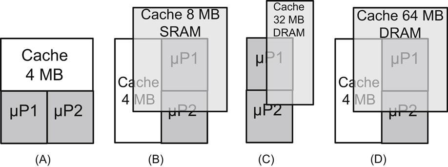
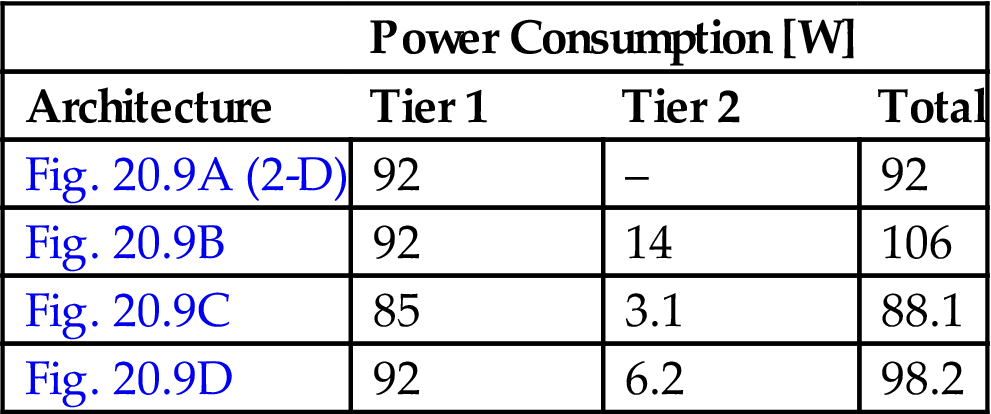
The presence of a second memory tier naturally increases the on-chip power consumption as compared to a 2-D microprocessor. The estimated power consumed by each configuration, shown in Fig. 20.9, is listed in Table 20.2. Despite the increase in power dissipation, the highest increase in temperature as compared to the baseline system does not exceed 5 °C with a maximum (and manageable) temperature of 92.9 °C [711,727].
Table 20.2
Power Dissipation of the 3-D Microprocessor Architectures [711]
| Power Consumption [W] | |||
| Architecture | Tier 1 | Tier 2 | Total |
| Fig. 20.9A (2-D) | 92 | – | 92 |
| Fig. 20.9B | 92 | 14 | 106 |
| Fig. 20.9C | 85 | 3.1 | 88.1 |
| Fig. 20.9D | 92 | 6.2 | 98.2 |
Larger on-chip memories can decrease cache miss rates for single or double core microprocessors [728]. For large scale systems with tens of cores, however, the memory access time and the related buss bandwidth can be a performance bottleneck. An on-chip network is an effective way to overcome these issues. 3-D architectures for NoC are therefore the subject of the following section.
20.3 3-D Networks-on-Chip
NoC is a design paradigm to enhance interconnections within complex integrated systems. These networks have an interconnect structure which provide Internet like communication among various elements of the network; however, on-chip networks differ from traditional interconnection networks in that communication among the network elements is achieved through the on-chip routing layers rather than the metal tracks of the package or printed circuit board (PCB).
NoC offer high flexibility and regularity, supporting simpler interconnect models and greater fault tolerance. The canonical interconnect backbone of the network combined with appropriate communication protocols enhance the flexibility of these systems [37]. NoC provide communication among a variety of functional intellectual property (IP) blocks or processing elements (PEs), such as processor and Digital signal processing (DSP) cores, memory blocks, FPGA blocks, and dedicated hardware, serving a plethora of applications that include image processing, personal devices, and mobile handsets, [729–731] (the terms IP block and PEs are interchangeably used in this chapter to describe functional structures connected by a NoC). The intra-PE delay, however, cannot be reduced by the network. Furthermore, the length of the communication channel is primarily determined by the area of the PE, which is typically unaffected by the network structure. By merging vertical integration with NoC, many of the individual limitations of 3-D ICs and NoC are circumvented, yielding a robust design paradigm with unprecedented capabilities.
Research in 3-D NoC has progressed considerably in the past few years where several 3-D topologies have been explored [732], and design methods and synthesis tools [733] have been published [503,734,735]. Several methodologies to manage vertical links with TSVs have also been reported [736].
Addo-Quaye [503] presented an algorithm for the thermal aware mapping and placement of 3-D NoC including regular mesh topologies. Li et al. [735] proposed a similar 3-D NoC topology employing a buss structure for communicating among PEs located on different physical tiers. Targeting multiprocessor systems, the proposed scheme in [735] considerably reduces cache latencies by utilizing the third dimension. Multidimensional interconnection networks have been studied under various constraints, such as constant bisection-width and pin-out constraints [706]. NoC differ from generic interconnection networks, however, in that NoC are not limited by the channel width or pin-out. Alternatively, physical constraints specific to 3-D NoC, such as the number of nodes that can be placed in the third dimension and the asymmetry in the length of the channels of the network, have to be considered.
In this chapter, various possible topologies for 3-D NoC are presented. Additionally, analytic models for the zero-load latency and power consumption with delay constraints of these networks that capture the effects of the topology on the performance of 3-D NoC are described [737]. Although these models are applied to mesh topologies, the interconnect models remain valid for other topologies as long as the parameters, such as the number of hops for a topology, are properly adapted to the features of the target topology. Optimum topologies are shown to exist that minimize the zero-load latency and power consumption of a network. These optimum topologies depend upon a number of parameters characterizing both the router and the communication channel, such as the number of ports of the network, the length of the communication channel, and the impedance characteristics of the interconnect. Several tradeoffs among these parameters that determine the minimum latency and power consumption topology of a network are described for different network sizes. A cycle accurate simulator for 3-D topologies is also discussed. This tool is used to evaluate the behavior of several 3-D topologies under broad traffic scenarios.
Several interesting topologies, which are the topic of this chapter, emerge by incorporating the third dimension in NoC. In the following section, several topological choices for 3-D NoC are reviewed. In Section 20.3.2, an analytic model of the zero-load latency of traditional interconnection networks is adapted for each of the proposed 3-D NoC topologies, while the power consumption model of these network topologies is described in Section 20.3.3. In Section 20.3.4, the 3-D NoC topologies are compared in terms of the zero-load network latency and power consumption with delay constraints, and guidelines for the optimum design of speed driven or power driven NoC structures are provided. An advanced NoC simulator, which is used to evaluate the performance of a broad variety of 3-D network topologies, is presented in Section 20.3.5.
20.3.1 3-D NoC Topologies
Several topologies for 3-D networks are presented and related terminology is introduced in this section. Mesh structures have been a popular network topology for conventional 2-D NoC [738,739]. A fundamental element of a mesh network is illustrated in Fig. 20.10A, where each PE is connected to the network through a router. A PE can be integrated either on a single physical tier (2-D IC) or on several physical tiers (3-D IC). Each router in a 2-D NoC is connected to a neighboring router in one of four directions. Consequently, each router has five ports. Alternatively, in a 3-D NoC, the router typically connects to two additional neighboring routers located on the adjacent physical tiers. The architecture of the router is considered here to be a canonical router with input and output buffering [740]. The combination of a PE and router is called a network node. For a 2-D mesh network, the total number of nodes N is N=n1×n2, where ni is the number of nodes included in the ith physical dimension.
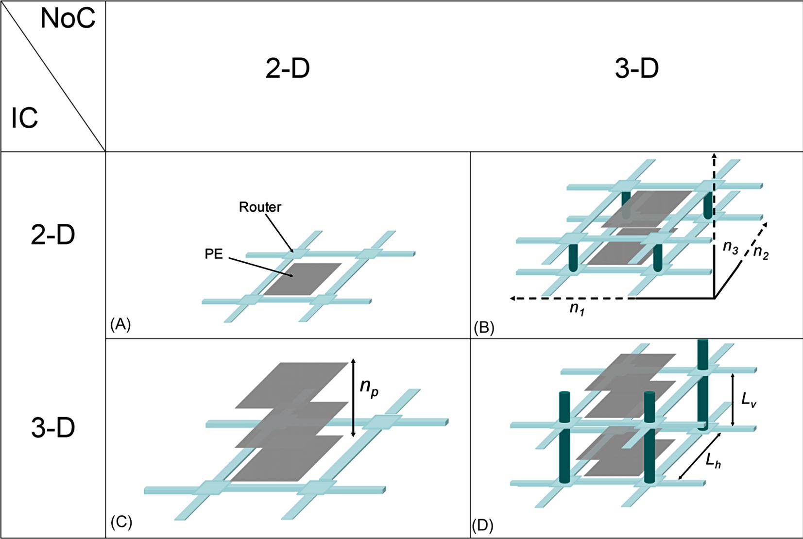
Integration in the third dimension introduces a variety of topological choices for NoCs. For a 3-D NoC as shown in Fig. 20.10B, the total number of nodes is N=n1×n2×n3, where n3 is the number of nodes in the third dimension. In this topology, each PE is on a single yet possibly different physical tier (2-D IC–3-D NoC). Alternatively, a PE can be implemented on only one of the n3 physical tiers of the system and, therefore, the 3-D system contains n1×n2 PEs on each one of the n3 physical tiers such that the total number of nodes is N. This topology is discussed in [503] and [735]. A 3-D NoC topology is illustrated in Fig. 20.10C, where the interconnect network is contained within one physical tier (i.e., n3=1), while each PE is integrated on multiple tiers, notated as np (3-D IC–2-D NoC). Finally, a hybrid 3-D NoC based on the two previous topologies is depicted in Fig. 20.10D. In this NoC topology, both the interconnect network and the PEs can span more than one physical tier within the stack (3-D IC–3-D NoC). In the following section, latency expressions for each of the NoC topologies are described, assuming a zero-load model.
20.3.2 Zero-Load Latency for 3-D NoC
In this section, analytic models of the zero-load latency of each of the 3-D NoC topologies are described. The zero-load network latency is widely used as a performance metric in traditional interconnection networks [741]. The zero-load latency of a network is the latency where only one packet traverses the network. Although such a model does not consider contention among packets, the zero-load latency model can be used to describe the effect of a topology on the performance of a network. The zero-load latency of an NoC with wormhole switching is [741]
(20.1)
where the first term is the routing delay, tc is the propagation delay along the wires of the communication channel, which is also called a buss here for simplicity, and the third term is the serialization delay of the packet. hops is the average number of routers that a packet traverses to reach the destination node, tr is the router delay, Lp is the length of the packet in bits, and b is the bandwidth of the communication channel defined as b ≡ wcfc, where wc is the width of the channel in bits and fc is the inverse of the propagation delay of a bit along the longest communication channel.
Since the number of tiers that can be stacked in a 3-D NoC is constrained by the target technology, n3 is also constrained. Furthermore, n1, n2, and n3 are not necessarily equal. The average number of hops in a 3-D NoC is
(20.2)
assuming dimension order routing to ensure that the minimum distance paths are used for the routing of packets between any source destination node pair. The number of hops in (20.2) can be divided into two components, the average number of hops within the two dimensions n1 and n2, and the average number of hops within the third dimension n3,
(20.3)
(20.4)
The delay of the router tr is the sum of the delay of the arbitration logic ta and the delay of the switch ts, which in this chapter is considered to be a classic crossbar switch [741],
(20.5)
The delay of the arbiter can be described from [742],
(20.6)
where p is the number of ports of the router and τ is the delay of a minimum sized inverter for the target technology. Note that (20.6) exhibits a logarithmic dependence on the number of router ports. The length of the crossbar switch also depends upon the number of router ports and the width of the buss,
(20.7)
where wt and st are, respectively, the width and spacing or, alternatively, the pitch of the interconnect and wc is the width of the communication channel in bits. Consequently, the worst case delay of the crossbar switch is determined by the longest path within the switch, which is equal to (20.7).
The delay of the communication channel tc is
(20.8)
where tv and th are, respectively, the delay of the vertical and horizontal channels (see Fig. 20.10B). Note that if n3=1, (20.8) describes the propagation delay of a 2-D NoC. Substituting (20.8) and (20.5) into (20.1), the overall zero-load network latency for a 3-D NoC is
(20.9)
To characterize ts, th, and tv, the models described in [743] are adopted, where repeaters implemented as simple inverters are inserted along the interconnect. According to these models, the propagation delay and rise time of a single interconnect stage for a step input, respectively, are
(20.10)
(20.11)
where ri (ci) is the per unit length resistance (capacitance) of the interconnect and li is the total length of the interconnect. The index i is used to notate the different interconnect delays included in the network (i.e., i ∈ {s,v,h}). hi and ki denote the number and size of the repeaters, respectively, and Cg0 and C0 represent, respectively, the gate and total input capacitance of a minimum sized device. C0 is the summation of the gate and drain capacitance of the device. Rd0 and Rr0 describe, respectively, the equivalent output resistance of a minimum sized device for the propagation delay and transition time of a minimum sized inverter where the output resistance is approximated as
(20.12)
K denotes a fitting coefficient and Idn0 is the drain current of an NMOS device at both Vds and Vgs equal to Vdd. The value of these device parameters are listed in Table 20.3. A 45 nm technology node is assumed and SPICE simulations of the predictive technology library are used to determine the individual parameters [252,432].
Table 20.3
Interconnect and Design Parameters, 45 nm Technology
| Parameter | Value | |
| NMOS | PMOS | |
| Wmin | 100 nm | 250 nm |
| Idsat/W | 1115 μΑ/μm | 349 μΑ/μm |
| Vdsat | 478 mV | −731 mV |
| Vt | 257 mV | −192 mV |
| A | 1.04 | 1.33 |
| Isub0 | 48.8 nA | |
| Ig0 | 0.6 nA | |
| Vdd | 1.1 Volts | |
| Temp. | 110°C | |
| Kd | 0.98 | |
| Kr | 0.63 | |
| Cg0 | 512 fF | |
| Cd0 | 487 fF | |
| τ | 17 ps | |

To include the effect of the input slew rate on the total delay of an interconnect stage, (20.10) and (20.11) are further refined by including an additional coefficient γ as in [744],
(20.13)
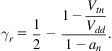 (20.13)
By substituting the subscript n with p, the corresponding value for a falling transition is obtained. The average value γ of γr and γf is used to describe the effect of the transition time on the interconnect delay. The overall interconnect delay can therefore be described as
(20.14)
where R0, a1, and a2 are described in [655] and the index i denotes the different interconnect structures such as the crossbar switch (i ≡ s), horizontal buss (i ≡ h), and vertical buss (i ≡ v).
For minimum delay, the size h and number k of repeaters are determined, respectively, by setting the partial derivative of ti with respect to hi and ki equal to zero and solving for hi and ki,
(20.15)
(20.16)
The expression in (20.14) only considers RC interconnects. An RC model is sufficiently accurate to characterize the delay of a crossbar switch since the length of the longest wire within the crossbar switch and the signal frequencies ensures that inductive behavior is not prominent. For the buss lines, however, inductive behavior can appear. For this case, suitable expressions for the delay and repeater insertion characteristics can be adopted from [655]. For the target operating frequencies (1 to 2 GHz) and buss length (<2 mm) considered in this chapter, an RC interconnect model provides sufficient accuracy [588]. Additionally, for the vertical buss, kv=1 and hv=1, meaning that no repeaters are inserted and minimum sized drivers are utilized. Repeaters are not necessary due to the short length of the vertical buss. Driving a buss with minimum sized inverters can affect the resulting minimum latency and power dissipation topology, as discussed in the following sections. Note that the latency expression includes the effects of the input slew rate. Additionally, since a repeater insertion methodology for minimum latency is applied, any further reduction in latency is due to the network topology.
The length of the vertical communication channel for the 3-D NoC shown in Fig. 20.10 is
(20.17a–c)
 (20.17a–c)
where Lv is the length of a through silicon (intertier) via connecting two routers on adjacent physical tiers. np is the number of physical tiers used to integrate each PE. The length of the horizontal communication channel is assumed to be
(20.18a,b)
where APE is the area of the PE. The area of all of the PEs and, consequently, the length of each horizontal channel are assumed to be equal. For those cases where the PE is placed in multiple physical tiers, a coefficient is included to consider the effect of the intertier vias on the reduction in the ideal wirelength due to utilization of the third dimension. The value of this coefficient (= 1.12) is based on the layout of a crossbar switch manufactured in the fully depleted silicon-on-insulator (FD-SOI) 3-D technology from MIT Lincoln Laboratory (MITLL) [307]. The same coefficient is also assumed for the PEs placed on more than one physical tier. In the following section, expressions for the power consumption of a network with delay constraints are presented.
20.3.3 Power Consumption in 3-D NoC
Power dissipation is a critical issue in 3-D circuits. Although the total power consumption of 3-D systems is expected to be lower than that of mainstream 2-D circuits (since the global interconnects are shorter [308]), the increased power density is a challenging issue for this novel design paradigm. Therefore, those 3-D NoC topologies that offer low power characteristics should be of significant interest.
The different power consumption components for interconnects with repeaters are briefly discussed in this section. Due to specified performance characteristics, a low power design methodology with delay constraints for the interconnect in an NoC is adopted from [655]. An expression for the total power consumption per bit of a packet transferred between a source destination node pair is used as the basis for characterizing the power consumption of an NoC for the 3-D topologies.
The power consumption components of an interconnect line with repeaters are:
a. Dynamic power consumption is the dissipated power due to the charge and discharge of the interconnect and input gate capacitance during a signal transition, and can be described by
(20.19)
where f is the clock frequency and as is the switching factor [745]. A value of 0.15 is assumed here; however, for NoC, the switching factor can vary considerably. This variation, however, does not affect the power comparison for the various topologies as the same switching factor is incorporated in each term for the total power consumed per bit of the network (the absolute value of the power consumption, however, changes).
b. Short-circuit power is due to the DC current path that exists in a CMOS circuit during a signal transition when the input signal voltage changes between Vtn and Vdd + Vtp. The power consumption due to this current is described as short-circuit power and is modeled in [746] by
(20.20)
where Id0 is the average drain current of the NMOS and PMOS devices operating in the saturation region and the value of the coefficients G and H are described in [747]. Due to resistive shielding of the interconnect capacitance, an effective capacitance is used in (20.20) rather than the total interconnect capacitance. This effective capacitance is determined from the methodology described in [748] and [749].
c. Leakage current power comprises two power components, the subthreshold and gate leakage currents. The subthreshold power consumption is due to current flowing during the cut-off region (below threshold), causing Isub current to flow. The gate leakage component is due to current flowing through the gate oxide, denoted as Ig. The total leakage current power can be described as
(20.21)
where the average subthreshold Isub0 and gate Ig0 leakage current of the NMOS and PMOS transistors is used in (20.21).
The total power consumption with delay constraint T0 for a single line of a crossbar switch Pstotal, horizontal buss Phtotal, and vertical buss Pvtotal is, respectively,
(20.22)
(20.23)
(20.24)
The power consumption of the arbitration logic is not included in (20.22), since most of the power is consumed by the crossbar switch and the buss interconnect, as discussed in [750]. Note that for a crossbar switch, the additional delay ta of the arbitration logic poses a stricter delay constraint on the power consumption of the switch, as shown in (20.22). The minimum power consumption with delay constraints is determined by the methodology described in [655], for which the optimum size h*powi and number k*powi of the repeaters for a single interconnect line is determined. Consequently, the minimum power consumption per bit between a source destination node pair in a NoC with a delay constraint is
(20.25)
The effect of resistive shielding is also considered in determining the effective interconnect capacitance. Furthermore, since the repeater insertion methodology in [655] minimizes the power consumed by the repeater system, any additional decrease in power consumption is due only to the network topology. In the following section, those 3-D NoC topologies that exhibit the maximum performance and minimum power consumption with delay constraints are presented. Tradeoffs in determining these topologies are discussed and the impact of the network parameters on the resulting optimum topologies are demonstrated for different network sizes.
20.3.4 Performance and Power Analysis for 3-D NoC
Several network parameters characterizing the topology of a network can significantly affect the speed and power of a system. The evaluation of these network parameters is discussed in subsection 20.3.4.1. The improvement in network performance achieved by the 3-D NoC topologies is explored in subsection 20.3.4.2. The distribution of nodes that produces the maximum performance is also discussed. The power consumption with delay constraints of a 3-D NoC and the topologies that yield the minimum power consumption of a 3-D NoC are presented in subsection 20.3.4.3.
20.3.4.1 Parameters of 3-D networks-on-chip
The physical layer of a 3-D NoC consists of different interconnect structures, such as a crossbar switch, the horizontal buss connecting neighboring nodes on the same physical tier and the vertical buss connecting nodes on different, not necessarily adjacent, physical tiers. The device parameters characterizing the receiver, driver, and repeaters are listed in Table 20.3. The interconnect parameters reported in Table 20.4 are different for each type of interconnect within a network.
Table 20.4
| Parameter | ||
| Interconnect Structure | Electrical | Physical |
| Crossbar switch | ρ = 3.07 μΩ-cm | w = 200 nm |
| kILD = 2.7 | s = 200 nm | |
| rs = 614 Ω/mm | t = 250 nm | |
| cs = 157.6 fF/mm | h = 500 nm | |
| Horizontal bus | ρ = 2.53 μΩ-cm | w = 500 nm |
| kILD = 2.7 | s = 250 (500) nm | |
| rh = 46 Ω/mm | t = 1100 nm | |
| ch = 332.6 (192.5) fF/mm | h = 800 nm | |
| a3-D = 1.02 (1.06) | − | |
| Vertical bus | ρ = 5.65 μΩ-cm | w = 1050 nm |
| rv = 51.2 Ω/mm | Lv = 10 μm | |
| cv = 600 fF/mm | – | |

A typical interconnect structure is shown in Fig. 20.11, where three parallel metal lines are sandwiched between two ground planes. This interconnect structure is considered for the crossbar switch (at the network nodes) where the intermediate metal layers are assumed to be utilized. The horizontal buss is implemented on the global metal layers and, therefore, only the lower ground plane is present in this structure for a 2-D NoC. For a 3-D NoC, however, the substrate (back-to-face tier bonding) or a global metal layer of an upper tier (face-to-face tier bonding) behaves as a second ground plane. To incorporate this additional ground plane, the horizontal bus capacitance is changed by the coefficient a3-D. A second ground plane decreases the coupling capacitance to an adjacent line, while the line-to-ground capacitance increases. The vertical buss is different from the other structures in that this buss uses through silicon vias. These intertier vias can exhibit significantly different impedance characteristics as compared to traditional horizontal interconnect structures, as discussed in [436] and also verified by extracted impedance parameters. The electrical interconnect parameters are extracted using a commercial impedance extraction tool [423], while the physical parameters are extrapolated from the predictive technology library [252], [432] and the 3-D integration technology developed by MITLL for a 45 nm technology node [307]. The physical and electrical interconnect parameters are listed in Table 20.4. For each of the interconnect structures, a buss width of 64 bits is assumed. In addition, n3 and np are constrained by the maximum number of physical tiers nmax that can be vertically stacked. A maximum of eight tiers is assumed. The constraints that apply for each of the 3-D NoC topologies shown in Fig. 20.10 are
(20.26a)
(20.26b)
(20.26c)
A small set of parameters is used as variables to explore the performance and power consumption of the 3-D NoC topologies. This set includes the network size or, equivalently, the number of nodes within the network N, the area of each PE APE, which is directly related to the buss length as described in (20.18), and the maximum allowed interconnect delay when evaluating the minimum power consumption with delay constraints. The range of values for these variables is listed in Table 20.5. Depending upon the network size, the NoC are roughly divided as small (N=16 to 64 nodes), medium (N=128 to 256 nodes), and large (N=512 to 2048 nodes) networks. For multiprocessor SoC networks, sizes of up to N=256 is expected to be feasible in the near future [735,751], whereas for NoC with a finer granularity, where the PEs each corresponds to hardware blocks of approximately 100,000 gates, network sizes over a few thousands nodes are predicted at the 45 nm technology node [752]. Note that this classification of the networks is not strict and is only intended to facilitate the discussion in the following sections.
20.3.4.2 Performance tradeoffs for 3-D NoC
The performance enhancements that can be achieved in NoC by utilizing the third dimension are discussed in this subsection. Each of the 3-D topologies decreases the zero-latency of the network by reducing different delay components, as described in (20.9). In addition, the distribution of network nodes in each physical dimension that yields the minimum zero-load latency is shown to significantly change with the network and interconnect parameters.
2-D IC–3-D NoC
Utilizing the third dimension to implement a NoC directly results in a decrease in the average number of hops for packet switching. The average number of hops on the same tier hops2-D (the intratier hops) and the average number of hops in the third dimension hops3-D (the intertier hops) are also reduced. Interestingly, the distribution of nodes n1, n2, and n3 that yields the minimum total number of hops is not always the same as the distribution that minimizes the number of intratier hops. This situation occurs particularly for small and medium networks, while for large networks, the distribution of n1, n2, and n3 which minimizes the hops also minimizes hops2-D.
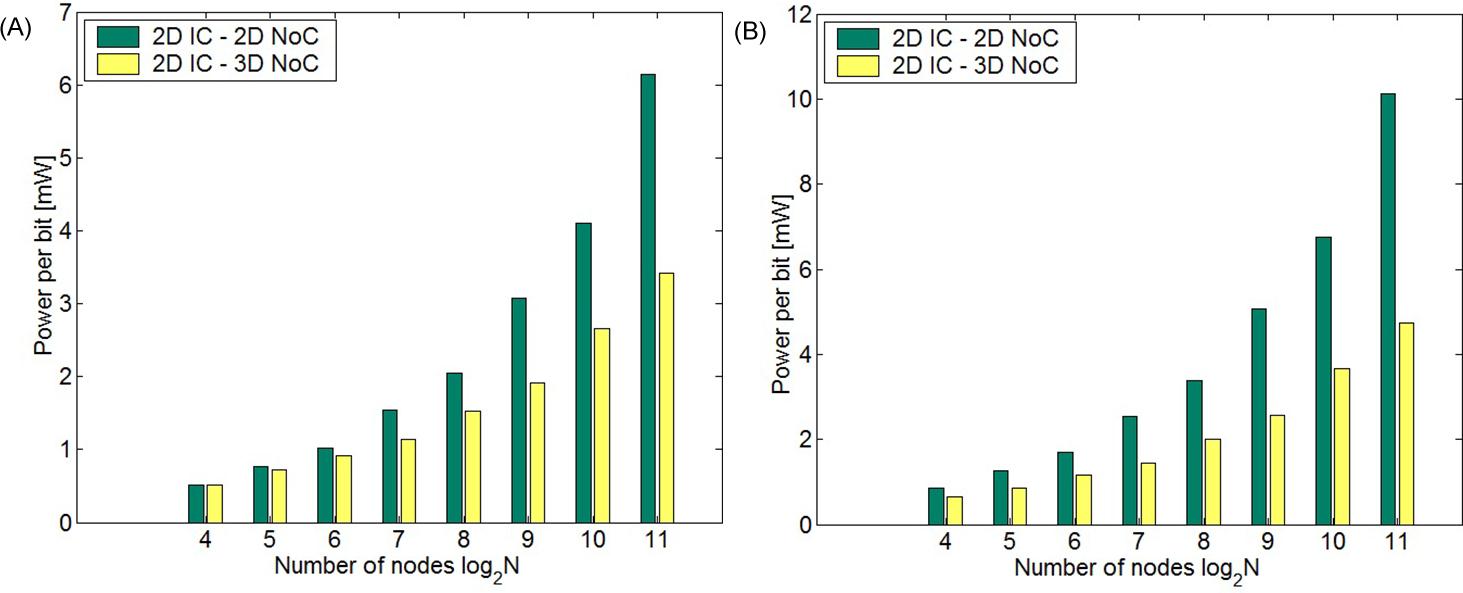
In a 3-D NoC, the number of router ports increases from five to seven, increasing, in turn, both the switch and arbiter delay. Furthermore, a short vertical buss generally exhibits a lower delay than a relatively long horizontal buss. In Fig. 20.12, the zero-load latency of the 2-D IC–3-D NoC is compared to that of the 2-D IC–2-D NoC for different network sizes. A decrease in latency of 15.7% and 20.1% can be observed for, respectively, N=128 and N=256 nodes with APE=0.81 mm2.
The node distribution that produces the lowest latency varies with network size. For example, n3max=8 is not necessarily the optimum for small and medium networks, although by increasing n3, more hops occur through the short, low latency vertical channel. This result can be explained by considering the reduction in the number of hops that originate from utilizing the third dimension for packet switching. For small and medium networks, the decrease in the number of hops is small and cannot compensate the increased routing delay due to the greater number of router ports in a 3-D NoC. As the horizontal buss length becomes longer, however, (e.g., approaching 2 mm), n3 > 1, and a slight decrease in the number of hops significantly decreases the overall delay, despite the increase in the routing delay for a 3-D NoC. As an example, consider a network with log2N=4 and APE=0.81 mm2. The minimum latency node distribution is n1 = n2=4 and n3=1 (identical to a 2-D IC–2-D NoC, as shown in Fig. 20.12), while for APE=4 mm2, n1=n2=2 and n3=4.
The optimum node distribution can also be affected by the delay of the vertical channel. The repeater insertion methodology for minimum delay as described in Section 20.3.2 can significantly reduce the delay of the horizontal buss by inserting large sized repeaters (i.e., h > 300). In this case, the delay of the vertical buss becomes comparable to that of the horizontal buss with repeaters. Consider a network with N=128 nodes. Two different node distributions yield the minimum average number of hops, specifically, n1=4, n2=4, and n3=8 and n1=8, n2=4, and n3=4. The first of the two distributions also results in the minimum number of intratier ![]() , thereby reducing the latency of the horizontal buss, as described by (20.9). Simulation results, however, indicate that this distribution is not the minimum latency node distribution, as the delay due to the vertical channel is nonnegligible. For this reason, the latter distribution with n3=4 is preferable since a smaller number of hops3-D occurs, resulting in the minimum network latency.
, thereby reducing the latency of the horizontal buss, as described by (20.9). Simulation results, however, indicate that this distribution is not the minimum latency node distribution, as the delay due to the vertical channel is nonnegligible. For this reason, the latter distribution with n3=4 is preferable since a smaller number of hops3-D occurs, resulting in the minimum network latency.
3-D IC–2-D NoC
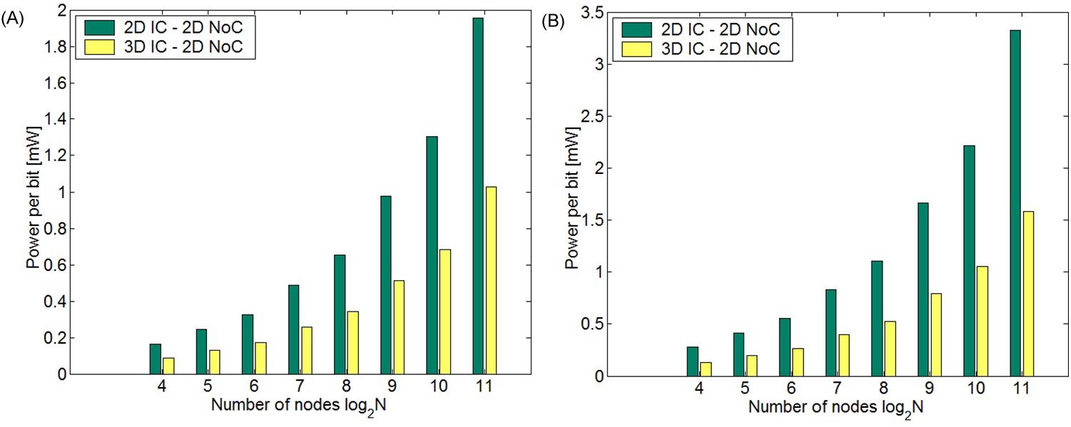
For this type of 3-D network, the PEs are allowed to span multiple physical tiers while the network effectively remains 2-D (i.e., n3=1). Consequently, the network latency is only reduced by decreasing the length of the horizontal buss, as described in (20.18). The routing delay component remains constant with this 3-D topology. Decreasing the horizontal buss length lowers both the communication channel delay and the serialization delay. In Fig. 20.13, the decrease in latency that can be achieved by a 3-D IC–3-D NoC is illustrated. A latency decrease of 30.2% and 26.4% can be observed for, respectively, N=128 and N=256 nodes with APE=2.25 mm2. The use of multiple physical tiers reduces the latency; therefore, the optimum value for np = nmax, regardless of the network size and buss length.
In Figs. 20.13A and 20.13B, the improvement in the network latency over a 2-D IC–2-D NoC for several network sizes and for different PE areas (i.e., different horizontal buss length) is illustrated for, respectively, the 2-D IC–3-D NoC and 3-D IC–2-D NoC topologies. Note that for the 2-D IC–3-D NoC topology, the improvement in delay is smaller for PEs with a larger area or, equivalently, with longer buss lengths independent of the network size. For longer buss lengths, the buss latency comprises a larger portion of the total network latency. Since for a 2-D IC–3-D NoC only the hop count is reduced, the improvement in latency is lower for longer buss lengths. Alternatively, the improvement in latency is greater for PEs with a larger area independent of the network size for 3-D IC–2-D NoC. This situation is due to the significant reduction in the PE area (or buss length) achieved with this topology. Consequently, there is a tradeoff in the latency of a NoC that depends both on the network size and the area of the PEs. In Fig. 20.14A, the improvement is not significant for small networks (all of the curves converge to approximately zero) in 2-D IC–3-D NoC while this situation does not occur for 3-D IC–2-D NoC. This behavior is due to the increase in the delay of the network router as the number of ports increases from five to seven for 2-D IC–3-D NoC, which is a considerable portion of the network latency for small networks. Note that for 3-D IC–2-D NoC, the network essentially remains 2-D and therefore the delay of the router for this topology does not increase. To achieve the minimum delay, a 3-D NoC topology that exploits these tradeoffs is described in the following subsection.

3-D IC–3-D NoC
This topology offers the greatest decrease in latency over the aforementioned 3-D topologies. The 2-D IC–3-D NoC topology decreases the number of hops while the buss and serialization delays remain constant. With the 3-D IC–2-D NoC, the buss and serialization delay is smaller but the number of hops remains unchanged. With the 3-D IC–3-D NoC, all of the latency components can be decreased by assigning a portion of the available physical tiers for the network while the remaining tiers of the stack are used for the PE. The resulting decrease in network latency as compared to a standard 2-D IC–2-D NoC and the other two 3-D topologies is illustrated in Fig. 20.15. A decrease in latency of 40% and 36% can be observed, respectively, for N=128 and N=256 nodes with APE=4 mm2. Note that the 3-D IC–3-D NoC topology achieves the greatest savings in latency by optimally balancing n3 with np.
For certain network sizes, the performance of the 3-D IC–2-D NoC is identical to either the 2-D IC–3-D NoC or 3-D IC–2-D NoC. This behavior occurs because for large network sizes, the delay due to the large number of hops dominates the total delay and, therefore, the latency can be primarily reduced by decreasing the average number of hops (n3=nmax). For small networks, the buss delay is large and the latency savings is typically achieved by reducing the buss length (np=nmax). For medium networks, though, the optimum topology is obtained by dividing nmax between n3 and np to ensure that (20.26c) is satisfied. This distribution of n3 and np as a function of the network size and buss length is illustrated in Fig. 20.16.

Note the shift in the value of n3 and np as the PE area APE or, equivalently, the buss length increases. For long busses, the delay of the communication channel becomes dominant and therefore the smaller number of hops for medium-sized networks cannot significantly decrease the total delay. Alternatively, further decreasing the buss length by placing the PEs within a greater number of physical tiers leads to a larger savings in delay.
The suggested optimum topologies for different network sizes (namely, small, medium, and large networks) also depend upon the interconnect parameters of the network. Consequently, a change in the optimum topology for different network sizes can occur when different interconnect parameters are considered. Despite the sensitivity of the topologies on the interconnect parameters, the tradeoff between the number of hops and the buss length for different 3-D topologies (see Figs. 20.14 and 20.16) can be exploited to improve the performance of an NoC. In the following subsection, the topology that yields the minimum power consumption while satisfying the delay constraints is described. The distribution of nodes for that topology is also discussed.
20.3.4.3 Power consumption in 3-D NoC
The different power consumption components for the interconnect within an NoC are described in Section 20.3.3. The methodology presented in [655] is applied here to minimize the power consumption of these interconnects while satisfying the specified operating frequency of the network. Since a power minimization methodology is applied to the buss lines, the power consumed by the network can only be further reduced by the choice of network topology. Additionally, the power consumption also depends upon the target operating frequency, as discussed later in this section.
As with the zero-load latency, each topology affects the power consumption of the network in a different way. From (20.25), the power consumption can be reduced by either decreasing the number of hops for the packet or by decreasing the buss length. Note that by reducing the buss length, the interconnect capacitance is not only reduced but also the number and size of the repeaters required to drive the lines are decreased, resulting in a greater savings in power. The effect of each of the 3-D topologies on the power consumption of an NoC is investigated in this section.
2-D IC–3-D NoC
Similar to the network latency, the power consumption is decreased in this topology by reducing the number of hops for packet switching. Again, the increase in the number of ports is significant; however, the effect of this increase is not as important as in the latency of the network. A 3-D network, therefore, can reduce power even in small networks. The power savings achieved with this topology is depicted in Fig. 20.17 for several network sizes, where the savings is greater in larger networks. This situation occurs because the reduction in the average number of hops for a 3-D network increases for larger network sizes. A power savings of 26.1% and 37.9% is achieved, respectively, for N=128 and N=512 with APE=1 mm2.
3-D IC–2-D NoC
With this topology, the number of hops in the network is the same as for a 2-D network. The horizontal buss length, however, is shorter since the PEs are placed in more than one physical tier. The greater the number of physical tiers that can be integrated into a 3-D system, the larger the power savings, meaning that the optimum value for np with this topology is always nmax regardless of the network size and operating frequency. The savings is limited by the number of physical tiers that can be integrated in a 3-D technology. The power savings for various network sizes are shown in Fig. 20.18. Note that for this type of NoC, the maximum performance topology is identical to the minimum power consumption topology, as the key element of both objectives originates solely from the shorter buss length. The savings in power is approximately 35% when APE=0.64 mm2 for every network size as the per cent reduction in the buss length is the same for each network size.
3-D IC–3-D NoC
Allowing the available physical tiers to be utilized either for the third dimension of the network or for the PEs, the 3-D IC–3-D NoC scheme achieves the greatest savings in power in addition to the minimum delay, as discussed in the previous subsection. The distribution of nodes along the physical dimensions, however, that produces either the minimum latency or the minimum power consumption for every network size is not necessarily the same. This nonequivalence is due to the different degree of importance of the average number of hops and the buss length in determining the latency and power consumption of a network. In Fig. 20.19, the power consumption of the 3-D IC–3-D NoC topology is compared to the previously discussed 3-D topologies. A power savings of 38.4% is achieved for N=128 with APE=1 mm2. For certain network sizes, the power consumption of the 3-D IC–3-D NoC topology is the same as the 2-D IC–3-D NoC and 3-D IC–2-D NoC topologies. For the 2-D IC–3-D NoC, the power consumption is less by reducing the number of hops for packet switching, while for the 3-D IC–2-D NoC, the NoC power dissipation is decreased by shortening the buss length. The former approach typically benefits small networks, while the latter approach dissipates less power in large networks. For medium sized networks and depending upon the network and interconnect parameters, nonextreme values for the n3 and np parameters (e.g., 1<n3<nmax and 1<np<nmax) are required to produce the minimum power consumption topology.

Note that this work emphasizes the latency and power consumption of a network, neglecting the performance requirements of the individual PEs. If the performance of the individual PEs is important, only one 3-D topology may be available; however, even with this constraint, a significant savings in latency and power can be achieved since in almost every case the network latency and power consumption can be decreased as compared to a 2-D IC–2-D NoC topology. Furthermore, as previously mentioned, if the available topology is the 2-D IC–3-D NoC, setting n3 equal to nmax is not necessarily the optimum choice.
The proposed zero-load network latency and power consumption expressions capture the effect of the topology; yet these models do not incorporate the effects of the routing scheme and traffic load. Alternatively, these models can be treated as lower bounds for both the latency and the power consumption of the network. Since minimum distance paths and no contention are implicitly assumed in these expressions, nonminimal path routing schemes and heavy traffic loads will increase both the latency and power consumption of the network. The routing algorithm is managed by the upper layers, other than the physical layer, comprising the communication protocol of the network. In addition, the traffic patterns depend upon the executed application of the network. The effect of each of the parameters on the performance of 3-D NoCs is explored in the following section by utilizing a network simulator.
20.3.4.4 Design aids for 3-D NoCs1
To evaluate the performance of emerging 3-D topologies for different applications, effective design aids are required. A network simulator that evaluates the effectiveness of different 3-D topologies is described in this section. Simulations of a broad variety of 3-D mesh- and torus-based topologies as well as traffic patterns are also discussed.
3-D NoC simulator
The core of the 3-D NoC simulator is based on the Worm_Sim NoC simulator [753], which has been extended to support 3-D topologies. In addition to 3-D meshes and tori, variants of these topologies are supported. Related routing schemes have also been adapted to provide routing in the vertical direction. An overview of the characteristics and capabilities of the simulator is depicted in Fig. 20.20.
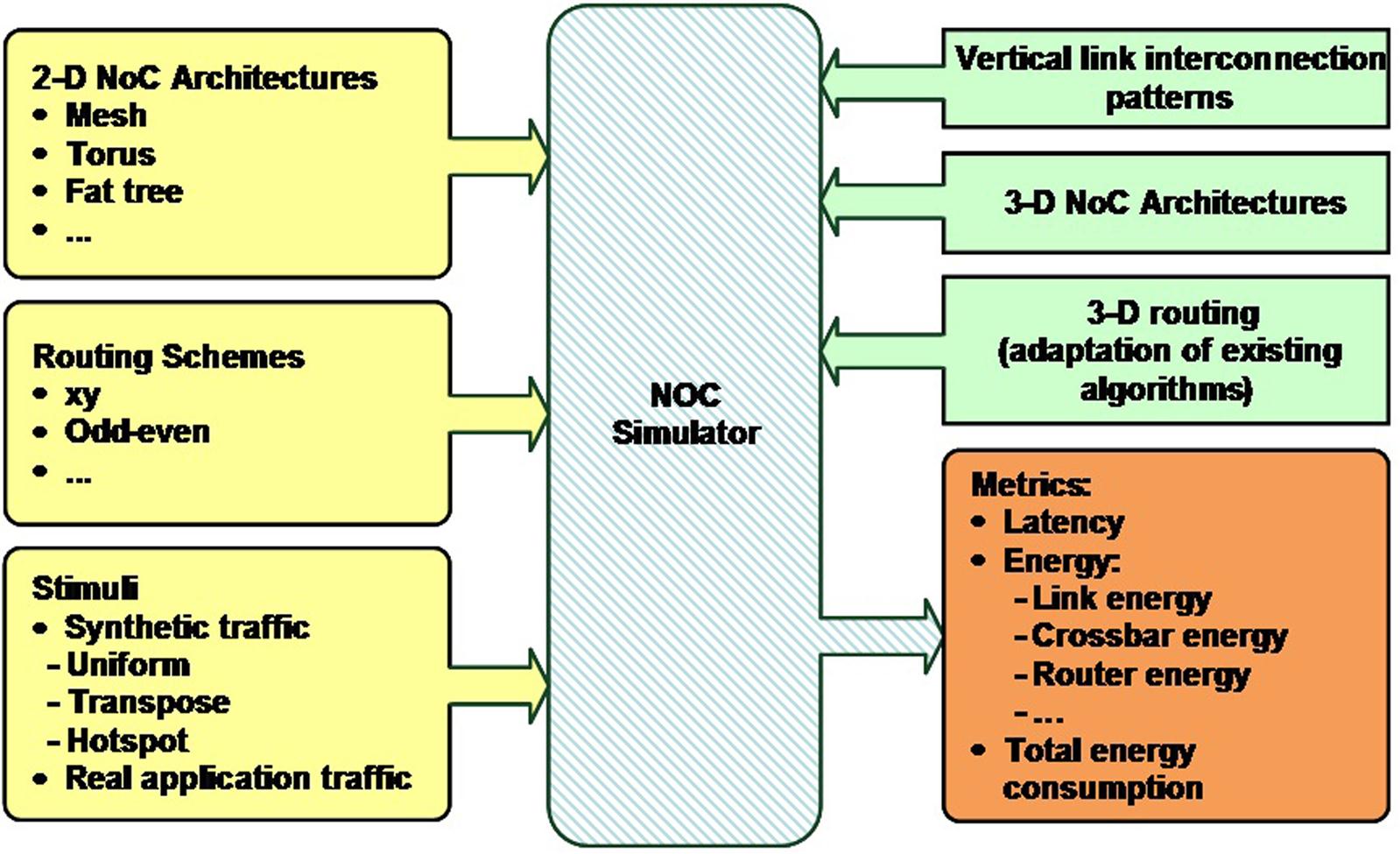
Several fundamental characteristics of a network topology are reported, including the energy consumption, average packet latency, and router area. The reported energy consumption includes the energy consumed by each component of the network, such as the crossbar switch and other circuitry within the network router, and the interconnect busses (i.e., link energy). Consequently, this simulator is a useful tool for exploring early decisions related to the system architecture.
An important capability of this tool is that variations of a basic 3-D mesh and torus topology can be efficiently explored. These topologies are characterized by heterogeneous interconnectivity, combining 2-D and 3-D network routers within the same network. The primary difference between these routers is that since a 3-D network router is connected to network routers on adjacent tiers, a 3-D router has two more ports than a 2-D network router. Consequently, a 3-D network router consumes a larger area and dissipates more power, yet provides greater interconnectivity.
Although these topologies typically have a greater delay than a straightforward 3-D topology, the savings in energy can be significant; in particular, those applications where speed is not the primary objective. Another application area that can benefit from these topologies is those applications where the data packets propagate over a small number of routers within the network. Alternatively, the spatial distribution of the required hops to propagate a data packet within the on-chip network is small. Since different applications can produce diverse types of traffic, an efficient traffic model is required. The simulator includes the traffic model used within the Trident tool [754]. This model consists of several parameters that characterize the spatial and temporal traffic across a network. The temporal parameter includes the number of packets and rate at which these packets are injected into a router. The spatial parameters include the distance that a packet travels within the network and the portion of the total traffic injected by each router into the network [754].
To generate these heterogeneous mesh and torus topologies, a distribution of the 2-D and 3-D routers needs to be determined. The following combinations of 2-D and 3-D routers for a 3-D mesh and torus are considered [755]:
Uniform: The 3-D routers are uniformly distributed over the different tiers. In this scheme, the 3-D routers are placed on each physical tier of the 3-D NoC. If no 2-D routers are inserted within the network, the topology is a 3-D mesh or torus (see Figs. 20.10 and 20.21B). In the case where both 2-D and 3-D routers are used within the network, the location of the routers on each tier is determined as follows:
• Place the first 3-D router on the (X, Y, Z) position of each tier.
• The four neighboring 2-D routers are placed in positions (X + r + 1, Y, Z), (X−r−1, Y, Z), (X, Y + r + 1, Z) and (X, Y−r−1, Z). The parameter r represents the periodicity (or frequency) of the 2-D routers within each tier. Consequently, a 2-D router is inserted every r 3-D routers in each direction within a tier. This scheme is exemplified in Fig. 20.21B, where one tier of a 3-D NoC with r=3 is shown.
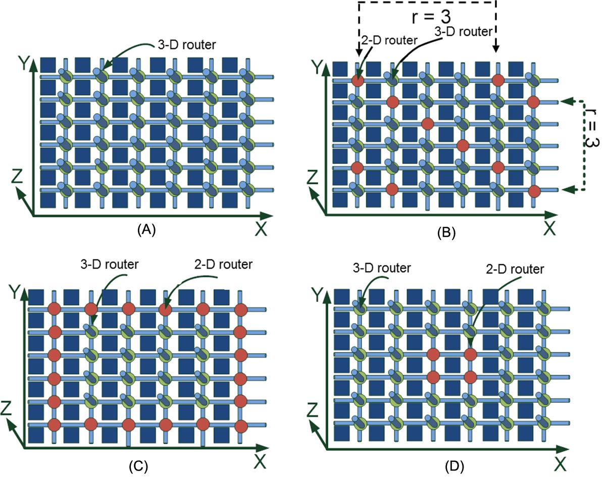
Center: The 3-D routers are located at the center of each tier, as shown in Fig. 20.21C. Since 3-D routers only exist at the center of a tier, only 2-D routers are placed along the outer region of each tier to connect the neighboring network nodes within the same tier.
Periphery: The 3-D routers are located at the periphery of each tier (see Fig. 20.21D). This combination is complementary to the Center placement.
Full Custom: The position of the 3-D routers is fully customized based on the requirements of the application, while minimizing the area occupied by the routers, since fewer 3-D routers are used. This configuration, however, produces an irregular structure that does not adapt well to changes in network functionality and application.
As illustrated in Fig. 20.20, different routing schemes are supported by the simulator. These algorithms are extended from the Worm_Sim simulator to support routing in the third dimension:
i. XYZ-OLD, which is an extended version of the shortest path XY routing algorithm.
ii. XYZ, which is based on XY routing where this algorithm determines which direction produces a lower delay, forwarding the packet in this direction.
iii. ODD–EVEN is the odd–even routing scheme as presented in [756]. In this scheme, the packets can take turns to avoid deadlock situations.
Consequently, the performance of a 3-D NoC can be evaluated under a broad and diverse set of parameters which reinforce the exploratory capabilities of the tool. In general, the following parameters of the simulator are configured:
• The NoC architecture, which can be a 2- or 3-D mesh or torus, where the dimensions of the network in the x, y, and z directions are, respectively, n1, n2, and n3.
• The type of input traffic and traffic load.
• The vertical link configuration file which defines whether a vertical link (required in 3-D routers) is present.
In the following section, several 3-D NoC topologies are explored under different traffic patterns and loads.
Evaluation of 3-D NoCs under different traffic scenarios
To compare the performance of 3-D topologies with conventional 2-D meshes and tori, two different network sizes with 64 and 144 nodes are considered. Each of these case studies is evaluated both in two and three dimensions. In two dimensions, the network nodes are connected to form 8×8 and 12×12 2-D, respectively, meshes and tori. Alternatively, the 3-D topologies of the target networks are placed on four physical tiers (i.e., n3=4). The dimensions of the two networks (n1×n2×n3), consequently, are, respectively, 4×4×4 and 6×6×4, respectively. Metrics for comparing the 2-D and 3-D topologies are the average packet latency, dissipated energy, and physical area. The area of the PEs is excluded since this area is the same in both 2-D and 3-D topologies. Topologies that contain PEs on multiple tiers (see Fig. 20.10C) are not considered in this analysis.
Although the 3-D topologies exhibit superior performance as compared to the 2-D meshes and tori, a topology that combines 2-D and 3-D routers can be beneficial for certain traffic patterns and loads. Using a fewer number of 3-D routers in a network results in smaller area and possibly power. This situation is due to the fewer number of ports required by a 2-D router, which has two fewer ports as compared to a 3-D router. Consequently, several combinations of 2-D and 3-D routers within a 3-D topology have been evaluated, some of which are illustrated in Fig. 20.21. Note that for each combination of 2-D and 3-D routers, the location of these routers within a 3-D on-chip network is the same on each tier of the network. In the case studies, ten different combinations of 2-D and 3-D routers are compared in terms of energy, delay, and area. These combinations are described below, where for the sake of clarity the number (and per cent in parenthesis) of 2-D and 3-D routers within a 4×4×4 NoC is provided:
• Full: All of the PEs are connected to 3-D routers [number of 3-D routers: 64 (100%)]. This combination corresponds to a fully connected mesh (see Fig. 20.10A) or torus 3-D network.
• Uniform-based: 2-D routers are connected to specific PEs within each tier of the 3-D network. The distribution of the 2-D routers is controlled by the parameter r, as discussed in the previous section. The chosen values are three (by_three), four (by_four), and five (by_five). The corresponding number of 3-D routers is: 44 (68.75%), 48 (75%), and 52 (81.25%). These combinations have a decreasing number of 2-D routers, approaching a fully connected 3-D mesh or torus.
• Odd: In this combination, all of the routers within a row are of the same type (i.e., either 2-D or 3-D). The type of router alternates among rows [number of 3-D routers: 32 (50%)].
• Edges: A portion of the PEs is located at the center of each tier and connected to 2-D routers with dimensions nx(2-D)×nx(2-D) while the remaining network nodes are connected to 3-D routers. For the example network, nx(2-D)=2 and, consequently, the number of 3-D routers is 48 (75%).
• Center: A segment of the PEs located at the center of each tier is connected to 3-D routers with dimensions nx(3-D)×nx(3-D) while the remaining PEs are connected to 2-D routers. For the example network, the number of 3-D routers is 16 (25%).
• Side-based: The PEs along a side (e.g., an outer row) of each tier are connected to 2-D routers. The combinations have the PEs along one (one_side), two (two_side), or three (three_side) sides connected to 2-D routers. The number of 3-D routers for each pattern, consequently, is, respectively, 48 (75%), 36 (56.25%), and 24 (37.5%). These combinations have an increasing number of 2-D routers, approaching the same number of routers as in a 2-D mesh or torus.
The interconnectivity for the two network sizes is evaluated under different traffic patterns and loads. The parameters of the traffic model used in the 3-D NoC simulator have been adjusted to produce the following common types of traffic patterns [757]:
• Uniform: The traffic is uniformly distributed across the network with the network nodes receiving approximately the same number of packets.
• Transpose: In this traffic scheme, packets originating from a node at location (a, b, c) reach the node at the destination (n1–a, n2–b, n3–c), where n1, n2, n3 are the dimensions of the network.
• Hot spot: A small number of network nodes (i.e., hot spot nodes) receive an increasing number of packets as compared to the majority of the nodes, which is modeled as uniformly receiving packets. The hot spot nodes within a 2-D NoC are positioned in the middle of each quadrant of the network. Alternatively, in a 3-D NoC, a hot spot is located in the middle of each tier.
The traffic loads are low, normal, and high. The heavy load has a 50% increase in traffic, whereas the low load has a 90% decrease in traffic as compared to a normal load.
The energy consumption in Joules and the average packet latency in cycles are compared for each of these patterns. The energy model of the NoC simulator is an architectural level model that determines the energy consumed by propagating a single bit across the network [758]. This model includes the energy of a bit through the various components of the network, such as the buffer and switch within a router and the interconnect buss among two neighboring routers. Note that only the dynamic component of the consumed energy is considered in this model [758]. Additionally, for each topology and combination of 2-D and 3-D routers, the total area of the routers is determined based on the gate equivalent of the switching fabric [759]. The objective is to determine which of these combinations results in higher network performance as compared to the 2-D and fully connected 3-D NoC. All of the simulations are performed for 200,000 cycles.
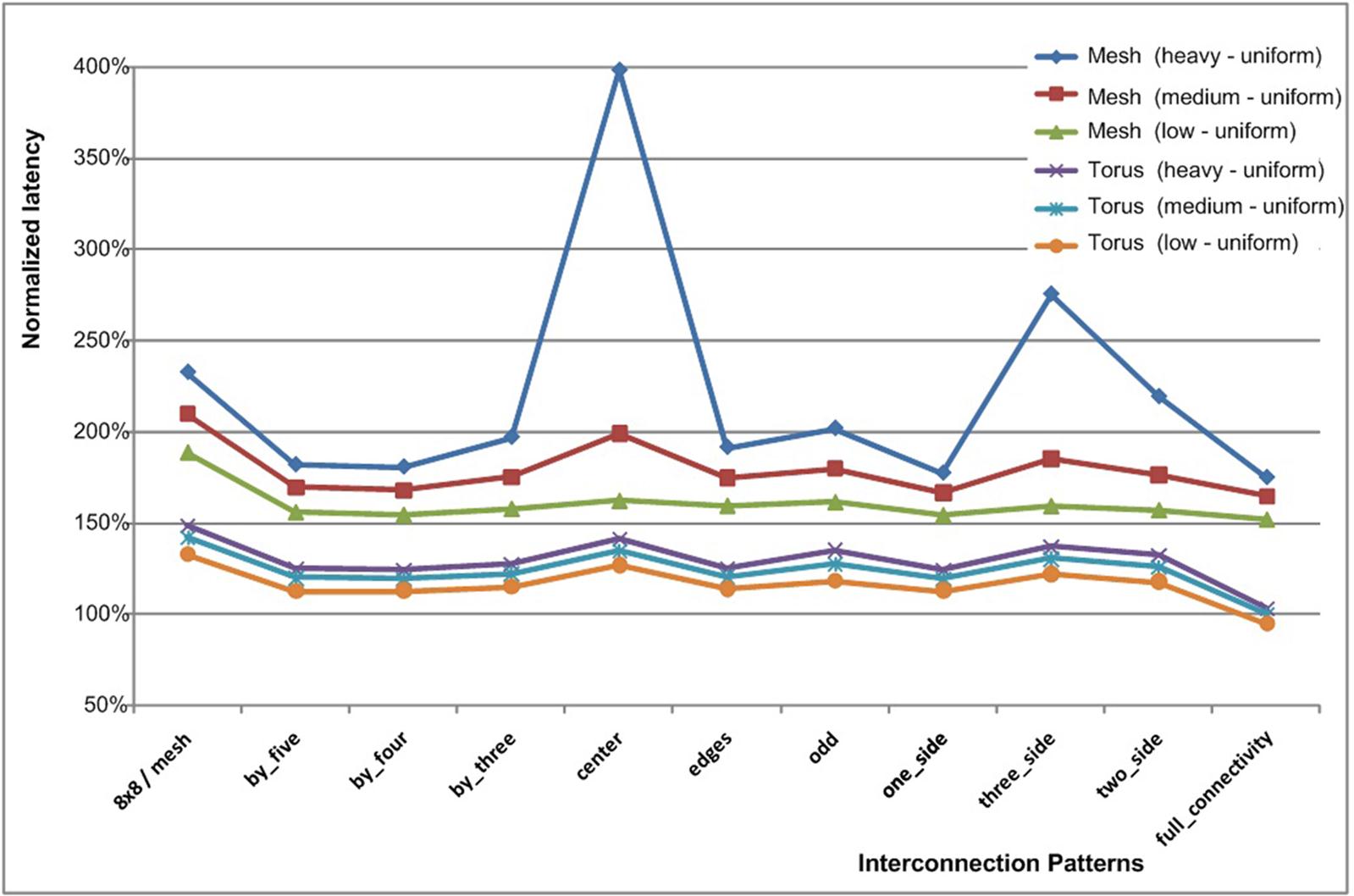
The average packet latency of the differently interconnected NoCs for a torus architecture is depicted in Fig. 20.22. The latency is normalized to the average packet latency of a fully connected 3-D NoC under normal load condition and for each traffic scheme. As expected, the network latency increases proportionally with traffic load.

Mesh topologies exhibit similar behavior, though the latency is higher due to the decreased connectivity as compared to the torus topologies. This behavior is depicted in Fig. 20.23, where the latency of a 64-node mesh and torus NoC are compared (the basis for the latency normalization is the average packet latency of a fully connected 3-D torus). The mesh topologies exhibit an increased packet latency of 34% as compared to the torus topology for the same traffic pattern, traffic load, and routing algorithm.
The results of employing partial vertical connectivity (i.e., a combination of 2-D and 3-D routers) within a 3-D mesh network with uniform traffic, medium traffic load, and XYZ-OLD routing are illustrated in Fig. 20.24. The energy consumption, average packet latency, router area, and percent of 2-D routers for the 4×4×4 and 6×6×4 mesh architectures are illustrated, respectively, in Figs. 20.24A and 20.24B. All of these metrics are normalized to a fully connected 3-D NoC.
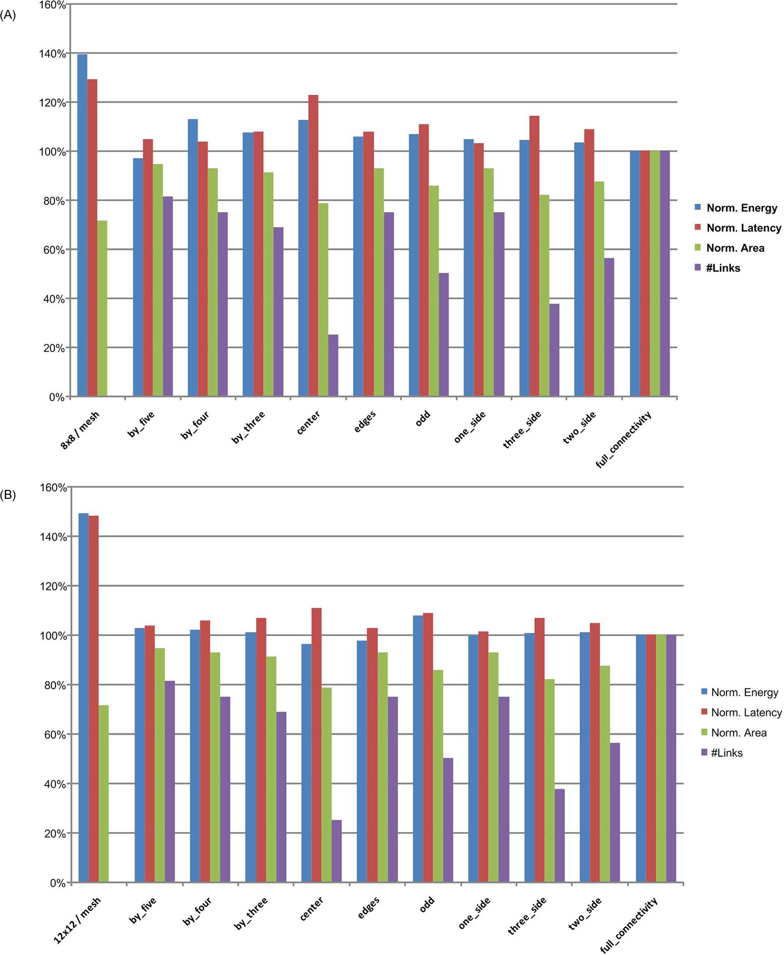
The advantages of a 3-D NoC as compared to a 2-D NoC are depicted in Fig. 20.24A. In this case, the 8×8 mesh dissipates 39% more energy and exhibits a 29% higher packet delivery latency as compared to a fully connected 3-D NoC. The overall area of the routers, however, is 71% of the area of a fully connected 3-D NoC, since all of the routers are 2-D. Employing the by_five combination results in a 3% reduction in energy and 5% increase in latency. In this combination, only 81% of the routers are 3-D, resulting in 5% smaller area for the switching logic. For a larger network (see Fig. 20.24B), several router combinations are superior to a fully connected 3-D NoC. Summarizing, the overall performance of a 2-D NoC is significantly lower, exhibiting an increased energy and latency of approximately 50%.
When the traffic load is increased by 50%, the performance of all of the router combinations degrades as compared to the fully connected 3-D NoC. This behavior occurs since in a 3-D NoC containing both 2-D and 3-D routers, a fewer number of 3-D routers is used to save energy, reducing, in turn, the interconnectivity within the network. This lower interconnectivity increases the number of hops required to propagate data packets, increasing the overall network latency.
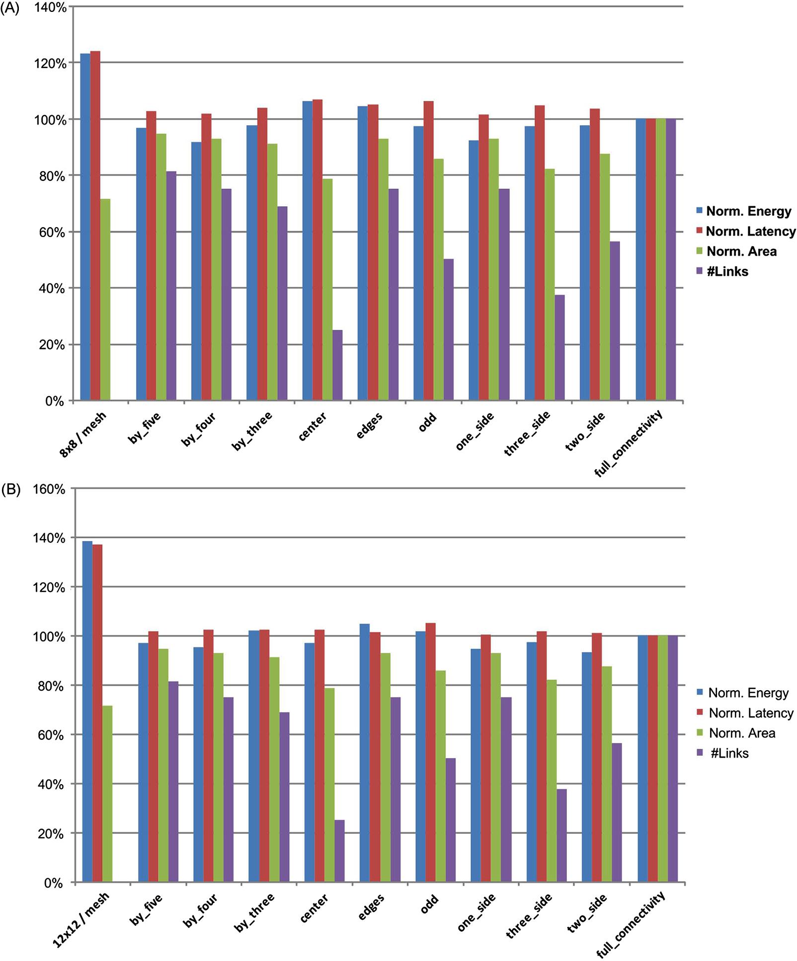
In the case of low traffic loads, alternative combinations can be beneficial since the requirements for communication resources are low. The simulation results for a 64 and 144 node 2-D and 3-D NoC under low uniform traffic and XYZ routing are illustrated in Fig. 20.25. An exception is the “edges” combination in the 64 node 3-D NoC (see Fig. 20.25A), where all of the 3-D routers reside along the edges of each tier within the 3-D NoC. This arrangement produces a 7% increase in packet latency. The performance of the 2-D NoC again decreases with increasing NoC dimensions. This behavior is depicted in Fig. 20.25B, where the 2-D NoC dissipates 38% more energy while the latency increases by 37%.
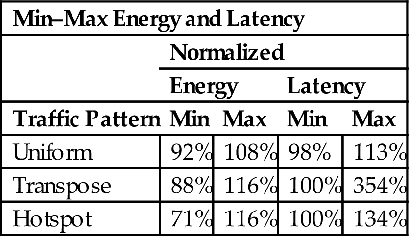
Finally, the energy and latency of the various interconnection patterns are compared to that of a fully connected 3-D NoC in Table 20.6. The three types of traffic are shown in the first column. The minimum and maximum value of the energy dissipation is listed in the next two columns. The minimum and maximum value of the average packet latency is, respectively, reported in the fourth and fifth column. Although only the latency increases, which is expected as the alternative interconnection patterns decrease the interconnectivity of the network, certain traffic patterns produce a considerable savings in energy. This savings in energy is important due to the significance of thermal effects in 3-D circuits. In addition to on-chip networks, another design style that greatly benefits from vertical integration is FPGAs, which is the topic of the following section.
Table 20.6
Min–Max Variation in 3-D NoC Latency and Power Dissipation as Compared to 2-D NoC under Different Traffic Patterns and a Normal Traffic Load
| Min–Max Energy and Latency | ||||
| Normalized | ||||
| Energy | Latency | |||
| Traffic Pattern | Min | Max | Min | Max |
| Uniform | 92% | 108% | 98% | 113% |
| Transpose | 88% | 116% | 100% | 354% |
| Hotspot | 71% | 116% | 100% | 134% |
20.4 3-D FPGAs
FPGAs are programmable ICs that implement abstract logic functions with a considerably smaller design turnaround time as compared to other design styles, such as application-specific (ASIC) or full custom ICs. Due to this flexibility, the share of the IC market for FPGAs has steadily increased. The tradeoff for the reduced time to market and versatility of the FPGAs is lower speed and increased power consumption as compared to ASICs. A traditional physical structure of an FPGA is depicted in Fig. 20.26, where the logic blocks (LB) can implement any digital logic function with some sequential elements and arithmetic units [760]. The switch boxes (SBs) provide the interconnections among the LBs. The SBs include pass transistors, which connect (or disconnect) the incoming routing tracks with the outgoing routing tracks. Memory circuits control these pass transistors and program the LBs for a specific application. In FPGAs, the SBs constitute the primary delay component of the interconnect delay between the LBs and can consume a great amount of power.
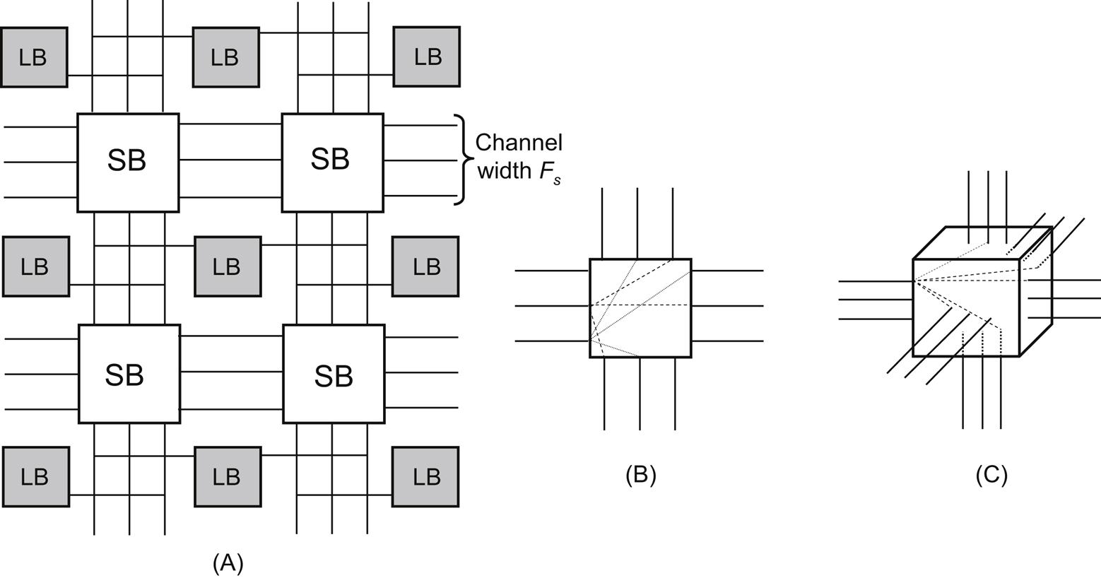
Extending FPGAs to the third dimension can improve performance while decreasing power consumption as compared to conventional planar FPGAs. A generalization of FPGAs to the third dimension would include multiple planar FPGAs, wafer or die bonded to form a 3-D system. The crucial difference between a 2-D and 3-D FPGA is that the SB provides communication to five LBs in a 3-D system rather than three neighboring LBs as in a 2-D FPGA (see Figs. 20.26B and 20.26C). Consequently, each incoming interconnect segment connects to five outgoing segments rather than three outgoing segments. The situation is somewhat different for the bottom and topmost tier of a 3-D FPGA, but in the following discussion, for simplicity this difference is neglected. Since the connectivity of a 3-D SB is greater, additional pass transistors are required in each SB, increasing the power consumption, memory requirements to configure the SB, and, possibly, the interconnect delay. The decreased interconnect length and greater connectivity can compensate, however, for the added complexity and power of the 3-D SBs.
To estimate the size of the array beyond which the third dimension is beneficial, the shorter average interconnect length offered by the third dimension and the increased complexity of the SBs should be simultaneously considered [761]. Incorporating the hardware resources (e.g., the number of transistors) required for each SB and the average interconnect length for a 2-D and 3-D FPGA, the minimum number of LBs for a 3-D FPGA to outperform a 2-D FPGA is determined from the solution of the following equation,
(20.27)
where Fs,2-D and Fs,3-D are, respectively, the channel width of a 2-D and 3-D FPGA, respectively, and N is the number of LBs. Solving (20.27) yields N=244, a number that is well exceeded in modern FPGAs.
Since the pass transistors, employed both in 2-D and 3-D SBs, contribute significantly to the interconnect delay, degrading the performance of an FPGA, those interconnects that span more than one LB can be utilized. These interconnect segments are named after the number of LBs that is traversed by these segments, as shown in Fig. 20.27. Wires that span two, four, or even six LBs are quite common in contemporary FPGAs. Interconnects that span one fourth to a half of an IC edge are also possible [762].
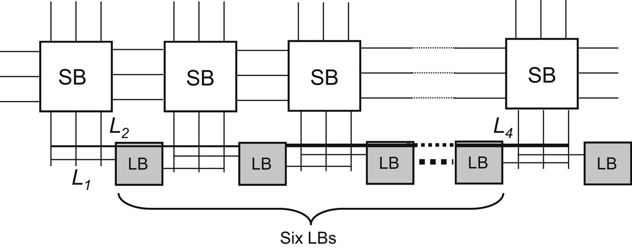
The opportunities that the third dimension offers in SRAM based 2-D FPGAs have also been investigated [763]. Analytic models that estimate the channel width in 2-D FPGAs have been extended to 3-D FPGAs. Hence, the channel width W for an FPGA with N LBs, exclusively consisting of unit length interconnect segments and implemented in n physical tiers, can be described by
(20.28)
 (20.28)
where f3-D(l) is a stochastic interconnect length distribution similar to those discussed in Chapter 7, Interconnect Prediction Models. χfpga converts a point-to-point distance into an interconnect length and et is the utilization parameter of the wiring tracks. These two factors can be determined from statistical data characterizing the placement and routing of benchmarks circuits on FPGAs. Note that these factors depend both on the architecture of the FPGA and the automated layout algorithm used to route the FPGA.
Several characteristics of FPGAs have been estimated from benchmarks circuits and randomized netlists placed and routed with the SEGment Allocator (SEGA) [764], the versatile place and route (VPR) [765] tools, and analytic expressions, such as (20.28). In these benchmark circuits, each FPGA is assumed to contain 20,000 four input LBs and is manufactured in a 0.25 μm CMOS technology. The area, channel density, and average wirelength are measured in LB pitches, which is the distance between two adjacent LBs, and are listed in Table 20.7 for different number of physical tiers.
Table 20.7
Area, Wirelength, and Channel Density Improvement in 3-D FPGAs
| Number of Tiers | Area (cm2) | Channel Density | Avg. Wirelength (LB Pitch) |
| 1 (2-D) | 7.84 | 41 | 8 |
| 2 (3-D) | 3.1 | 24 | 6 |
| 3 (3-D) | 1.77 | 20 | 5 |
| 4 (3-D) | 1.21 | 18 | 5 |

The improvement in the interconnect delay with a length equal to the die edge is depicted in Fig. 20.28 for different number of tiers. Those wires that span multiple LBs use unit length segments (i.e., no SBs are interspersed along these wires) whereas the die edge long wires use interconnect segments with a length equal to a quarter of the die edge. A significant decrease in delay is projected; however, these gains diminish for more than four tiers, as indicated by the saturated portion of the delay curves depicted in Fig. 20.28. The components of the power dissipated in a 3-D FPGA assuming a 2.5 volt power supply are shown in Fig. 20.29. The power consumed by the LBs remains constant since the structure of the LBs does not vary with the third dimension. However, due to the shorter interconnect length, the power dissipated by the interconnects is less. This improvement, however, is smaller than the improvement in the interconnect delay, as indicated by the slope of the curves illustrated in Figs. 20.28A and 20.28B. This behavior is attributed to the extra pass transistors in a 3-D SB, which increase the power consumption, compromising the benefit of the shorter interconnect length. Due to the reduced interconnect length, the power dissipated by the clock distribution network is also less.


20.5 Summary
Different classes of circuit structures that can greatly benefit from 3-D integration are described in this chapter. Several architectures and related designs aids for these circuits are discussed. The primary points of this discussion can be summarized as follows:
• Vertical integration can improve both the latency and power consumption of wire limited and communication centric circuits. These circuits include the microprocessor memory system, on-chip networks, and FPGAs.
• Implementing several components of a microprocessor across multiple physical tiers decreases the power consumption and improves the speed by utilizing fewer redundant pipeline stages.
• Partitioning a cache memory into a 3-D structure can reduce the time required to access the memory.
• Stacking additional memory tiers on a microprocessor can improve the overall performance of a microprocessor memory system without exceeding the thermal budget of the system.
• 3-D NoC are a natural evolution of 2-D NoC and exhibit superior performance.
• The minimum latency and power consumption can be achieved in 3-D NoC by reducing both the number of hops per packet and the length of the communications channels.
• Expressions for the zero-load network latency and power consumption are described for 3-D NoC.
• NoC implemented by a 3-D mesh reduce the number of hops required to propagate a data packet between two nodes within a network.
• 2-D IC–3-D NoC decrease the latency and power consumption by reducing the number of hops.
• 3-D IC–2-D NoC decrease the latency and power consumption by reducing the buss length or, equivalently, the distance between adjacent network nodes.
• Large networks are primarily benefited by the 2-D IC–3-D NoC topology, while small networks are enhanced by the 3-D IC–2-D NoC topology.
• The distribution of nodes corresponding to either the minimum latency or power consumption of a network depends upon both the interconnect parameters and network size.
• A tradeoff exists between the number of tiers utilized for a network and the number of PEs. Consequently, and not surprisingly, the 3-D IC–3-D NoC topology achieves the greatest improvement in latency and power consumption by most effectively exploiting the third dimension.
• A simulator that supports the exploration of 3-D NoC topologies with different routing schemes, traffic patterns, and traffic loads has been developed.
• A multi-tier on-chip network that includes both 2-D and 3-D routers can produce a significant savings in energy and area with a tolerable increase in latency as compared to a full 3-D topology.
• 3-D FPGAs have been proposed to improve the performance of 2-D FPGAs, where multiple planar FPGAs are bonded to form a 3-D stack of FPGAs.
• A critical issue in 3-D FPGA is the greater complexity of the 3-D SB that can negate the benefits from the shorter interconnect length and enhanced connectivity among the LBs.