
Synchronization in Three-Dimensional ICs
Abstract
The important issue of synchronization is the topic of this chapter. Clock tree synthesis (CTS) techniques under diverse design objectives for multi-tier systems are described. As these techniques extend CTS methods for planar circuits to three-dimensional (3-D) structures, standard algorithms and methods used in the synthesis of planar clock trees are presented. These techniques include the method of means and medians and the deferred-merge embedding method. A review of global clock distribution networks for 3-D circuits follows. Synthesis techniques for 3-D clock trees are extensively described. The last part of this chapter is dedicated to practical issues in the CTS process for 3-D circuits including, for example, fault tolerance for through silicon via defects.
Keywords
3-D clock tree synthesis; 3-D global clock networks; TSV fault tolerance; pre-bond testable clock trees
The clock signal constitutes the cornerstone of synchronous integrated systems as this signal provides the timing reference to maintain correct temporal operation. An important step in the delivery of the clock signal is the design of the clock distribution network, which for the majority of modern integrated systems includes a hierarchical clock network topology with several distribution levels [574]. Higher integration densities, larger silicon area, increasing power consumption, and process and environmental variability are some of the primary reasons that have led to multiple clock domains within modern integrated systems [264]. Consequently, the problem of distributing the clock signal in these complex systems can be described as the task of delivering a robust and reliable clock signal to all clock sinks (e.g., flip flops) across a circuit block, which can be as large as a processing core, or across a clock domain under skew, slew, power, and wiring constraints. Depending upon the performance specifications of the system, the significance of these constraints can vary, meaning that the design space changes according to the system specifications.
In hierarchical clock networks, the uppermost level of the hierarchy spans a large area and is often achieved with a symmetric topology requiring equidistant paths. These paths have the same traits (e.g., latency and slew) from the source to the roots of the next level of the clock network hierarchy. The global networks consist of several different topologies, such as H-tree, X-tree, ring, and mesh/grid topologies [575,576]. These global topologies often end at predetermined and reserved locations distributed throughout the system. Alternatively, the lower levels of the hierarchy connect to the clock pins of the circuit cells, where there can be several thousand clock sinks at each hierarchical level. A synthesized clock tree with specific timing characteristics typically provides the clock signal to all of these sinks. A multitude of clock tree synthesis (CTS) algorithms have been published over the past few decades that are supported by design automation tools for 2-D circuits.
With the advent of 3-D ICs, several efforts have focused on clock networks in three physical dimensions. The requirements for these 3-D clock synthesis techniques stem from the vertical interconnects (i.e., the through silicon vias (TSV)). The impedance characteristics of the TSV differ considerably from those of the horizontal wires and the partial clock networks that exist in each tier of a 3-D stack make pre-bond test a challenging task.
The design of 3-D clock network topologies is the topic of this chapter where both global topologies along with 3-D CTS algorithms are reviewed. Certain algorithms for the synthesis of two-dimensional (2-D) clock trees have been employed in the development of 3-D CTS methods. These algorithms are discussed in Section 15.1. The design and performance of 3-D global clock distribution networks are presented in Section 15.2. Synthesis techniques for 3-D clock trees are compared in Section 15.3. Enhanced techniques that stress practical issues relating to the synthesis of 3-D clock trees are reviewed in Section 15.4. The primary concepts of this chapter are summarized in Section 15.5. Note that most of the results described in this chapter are based on simulations and models while silicon measurements from an example test circuit characterizing the performance of global 3-D clock distribution networks are presented in Chapter 16, Case Study: Clock Distribution Networks for Three-Dimensional ICs.
15.1 Synthesis Techniques for Planar Clock Distribution Networks
Synthesis techniques for clock distribution networks have evolved significantly over the past several decades, producing clock network topologies that satisfy several design objectives and constraints [577,578–582]. Among these methods, some early techniques, including the methods of means and medians (MMM) [578] and deferred-merge embedding (DME) [581], have been extended to 3-D clock distribution networks. Consequently, these two techniques are discussed in this section, providing the necessary background to better follow the sections dedicated to the synthesis of 3-D clock network topologies.
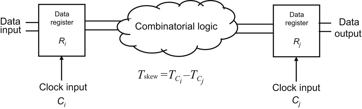
CTS techniques generate routed paths for a large number of clock sinks while ensuring a target clock skew is satisfied along with wirelength, clock slew, and power constraints. More precisely, clock skew is the difference between the clock signal arrival time of sequentially-adjacent registers [574]. Two registers are sequentially-adjacent if these registers are connected with combinatorial logic (i.e., no additional registers intervene between sequentially-adjacent registers). An illustration of this data path is provided in Fig. 15.1. An expression for the clock skew Tskew between these registers is also shown in Fig. 15.1, where TCi and TCj are, respectively, the arrival time of the clock signal at register Ri and Rj.
Other design objectives, such as robustness and reliability, are also used to enhance manufacturing technologies at the nanometer scale [584,585]. Minimizing any of these objectives typically entails tradeoffs with other design requirements due to the interdependence of the clock network characteristics. Consequently, synthesis methods ensure that design specifications are satisfied for all of the targeted objectives. For a large number of CTS methods, clock skew is the primary objective, where both zero skew and bounded skew algorithms have been developed [579,586]. Both the MMM and DME techniques discussed in this section focus on clock skew.
15.1.1 Method of Means and Medians
The MMM algorithm iteratively divides the clock sinks within a routing grid (or plane) with the use of cuts (i.e., bipartitions) in the x and y directions, producing two new sets of clock sinks for each cut. Assuming a set of m clock sinks, each clock sink is notated as si with coordinates (xi, yi) in the routing plane. The clock sinks can be described by the finite set ![]() . The location of the center of mass for this set is
. The location of the center of mass for this set is
(15.1)
 (15.1)
(15.2)
 (15.2)
where these coordinates constitute the root of the clock tree. To proceed with the cuts along the physical directions, an ordering of the clock sinks is utilized. Two different orderings of the clock sinks are formed by separately considering the x and y coordinates of the clock sinks in increasing order, meaning that for each element of a subset Sx(S) of the set, si precedes sj in Sx(S) if xi≤xj. A similar rule applies to the subset Sy(S) with respect to the y-coordinate. With these orderings, four different subsets are defined around the median of each ordering,
(15.3)
(15.4)
(15.5)
(15.6)
These four subsets are produced by applying a cut at the median of each ordering along each direction. All of these subsets contain approximately the same number of clock sinks as | |SL|–|SR| |≤1. The same inequality applies to the subsets SB and ST. The center of mass is determined for each of these new subsets. The algorithm connects these newly determined points with the center of the mass of the initial set S, which is the root of the tree. This process is repeated, producing two sets, left (L) and right (R), for each x-cut and bottom (B) and top (T) sets for each y-cut. The process terminates when each new set includes only a single clock sink.
A simple example of this algorithm is shown in Fig. 15.2, where routes between the center of mass for different sets are noted. Although routes between a center of mass and a subsequent center of mass, determined by a cut in the next iteration, are of equal length, different route lengths can occur as the algorithm progresses, as depicted in Fig. 15.2A. To address this situation, two pairs of cuts are applied. The pair of cuts leads to lower skew. This look-ahead procedure yields superior routings. As shown in Fig. 15.2B, the tree resulting from the y- and x-cuts exhibits a lower skew as compared to the tree shown in Fig. 15.2A. The complexity of the algorithm, including the look-ahead function, is O(m log m).

The MMM method ensures that after each iteration where cuts are performed, the routing path to the center of mass of the newly formed subsets is of equal length, leading to low (or zero) skew. This routing, however, is typically longer than the length of the minimum rectilinear Steiner tree (RMST) with the same set of clock sinks [403]. As described in [578], the wirelength of the generated clock tree increases proportionally to 3/2![]() , while for RMST, the length of the tree grows as
, while for RMST, the length of the tree grows as ![]() for m points (i.e., clock sinks) uniformly distributed across a routing grid. The ratio between the two routing algorithms increases by a constant factor of approximately 1.5×, demonstrating that the wirelength overhead of the MMM method is not excessive.
for m points (i.e., clock sinks) uniformly distributed across a routing grid. The ratio between the two routing algorithms increases by a constant factor of approximately 1.5×, demonstrating that the wirelength overhead of the MMM method is not excessive.
To limit this additional overhead, the MMM method is used in two phases. In the first phase, where the generated cut subsets include a large number of clock sinks, the routing proceeds with the MMM method. In the second phase, where the number of clock sinks within each subset produced at later iterations is small, standard routing algorithms are preferable to guarantee minimum wirelength with a low and acceptable increase in clock skew. The depth of the tree (or number of iterations) after which a routing technique other than MMM is applied depends upon the skew that can be tolerated.
15.1.2 Deferred-Merge Embedding Method
Another popular technique that has been extended to support the synthesis of 3-D clock networks is the DME method, which is a two phase CTS technique [581,582]. The input to the method is the connectivity of the sinks within some topology (typically a tree), where the location of the sinks is known and the internal nodes are placed to ensure that zero skew is achieved at minimum wirelength (assuming a linear delay model) [581]. Consequently, the DME technique produces optimal zero skew clock networks assuming a linear delay model, while suboptimal clock trees are produced if other more complex delay models, such as the Elmore delay model, are utilized. In this case, although the results are suboptimal, these results are in general of high quality, yielding zero skew clock trees with low wirelength. The advantage of the DME method is that as compared to MMM, the wirelength is minimized in addition to constructing a zero skew clock network.
The DME technique is not constrained by the topology of the clock network and, therefore, can be applied as a post-processing step once the internal nodes of a clock tree have, for example, been generated by the MMM method. Note, however, that the choice of topology or the choice of technique to generate the clock network affects the quality of the results produced by the DME method (i.e., the total wirelength since zero skew is guaranteed).
The DME method consists of a bottom-up and a top-down phase. In the bottom-up phase the feasible placement locations of each internal node are determined. Each internal node is a parent node for the root of (two) merged subtrees. In the top-down phase, the internal nodes are embedded into one of these feasible locations, ensuring that minimum wirelength is achieved (for the linear delay model) in addition to guaranteeing zero skew for all of the sinks within the clock network.
To explain this method, some related terminology is introduced. In the MMM method, a finite set S containing m clock sinks and the corresponding location of these sinks are considered as input. A clock tree notated as T(S) is embedded by the DME method in the Manhattan plane, where the location of each internal node of the tree is determined to ensure that the skew is zero and the wirelength of the clock tree is minimum. The placement of each node is denoted as pl(u). Assuming that u is the parent node of another node w, ew denotes the directed edge from the parent to the child node. The cost of this edge is notated as |ew|. As the Manhattan plane embeds the clock network, this cost is equal (or larger) to the Manhattan distance between these two nodes. Accordingly, the cost of the entire tree T(S) is the sum of the wirelength of all of these edges.
Similarly, the delay of any path from source node u to node w is notated as td(su,sw). The clock skew between two paths from the same source node is described by |td(su,sw)–td(su,sv)|. Assuming the root of the clock network is sr, the clock skew of T(S) is the maximum difference |td(sr,si)–td(sr,sj)| among all pairs of sinks si, sj belonging to S. If the linear delay model is used to estimate the delay of each source-sink path, this delay is the summation of the edges constituting the path from a source node u to a sink node w,
(15.7)
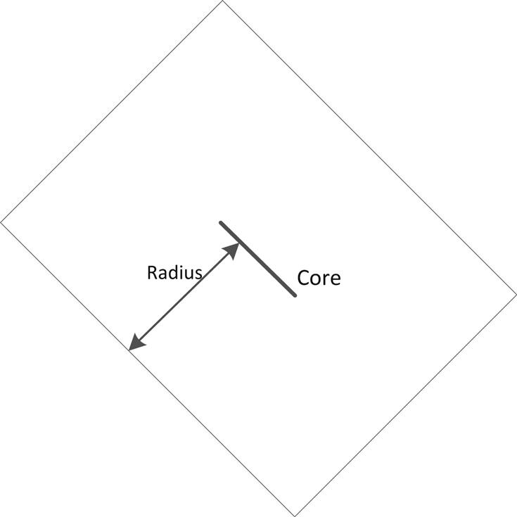
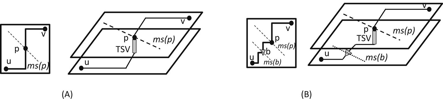
In addition to this notation, some other definitions are required to describe the DME method. The loci for each internal node determined during the bottom-up step are called merging segments. The merging segments are line segments with slope ±1 or, alternatively, with an angle of ±45° from the x–y routing directions. Similarly, a set of points on the Manhattan plane within a fixed distance from a Manhattan arc forms a tilted rectangular region (TRR), which is inscribed within Manhattan arcs. An example of a TRR is illustrated in Fig. 15.3, where the core arc and radius of the TRR are also shown. The core arc consists of all points located farthest from the boundary of the TRR (always assuming a Manhattan distance).
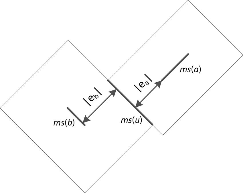
Considering a node u, the merging segment ms(u) for this node is determined as follows. If u belongs to S, the merging segment is the location of the clock sink; otherwise, u is an internal node and the length and position of the merging segment depend on the merging segments of the children nodes of u. Assuming that nodes a and b are the children nodes of u and since this step proceeds in a bottom-up manner, the merging segments of nodes a and b, notated, respectively, as ms(a) and ms(b) are known and are also Manhattan arcs [581]. This situation is illustrated in Fig. 15.4. The merging segment of node u is also a Manhattan arc and is obtained by intersecting two TRRs that have as core the segments ms(a) and ms(b). Consequently, ms(u) is formally described as ms(u)=TRRa∩TRRb. The radius of TRRa and TRRb is, respectively, |ea| and |eb|, as also shown in the figure. The merging cost for the subtrees rooted at nodes a and b is |ea|+|eb|. The objective is to determine these radii (i.e., |ea| and |eb|) such that the merging cost is minimized and the constraint of zero skew is satisfied.
Assuming a linear delay model, the lower bound for the merging cost is equal to the minimum Manhattan distance between ms(a) and ms(b), denoted as MDmin=d(ms(a), ms(b)). If the delay of nodes a and b is highly unbalanced, the merging cost deviates from this minimum to satisfy the zero skew requirement and may require additional wiring. The requirement of zero skew at node u can be satisfied from
(15.8)
where tld(a) and tld(b) denote, respectively, the (linear model) delay to the sinks of the subtrees rooted at nodes a and b. Note that since the zero skew requirement is satisfied at each level of the tree, these delays are the same at each sink of the subtrees from these nodes. The radius of TRRa and TRRb is obtained by letting |ea|+|eb|=MDmin, and if |tld(a)−tld(b)|≤MDmin,
(15.9)
and
(15.10)
If the condition |tld(a)−tld(b)|≤MDmin is not satisfied, additional wirelength is required to balance the skew from node u to nodes a and b, increasing the merging cost.
The bottom-up phase recursively merges the nodes of T(S) until the root node sr is reached. The clock driver is often placed at a specific location which is not intercepted by the merging segment of the root node. An additional segment connects to sr without degrading the performance of the resulting tree. The bottom-up phase (i.e., deferred-merge) terminates when the merging segment for the root node is obtained.
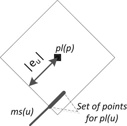
The top-down phase (i.e., embedding) follows. The exact placement of each node pl(u) is successively determined starting from the root node. For sr, any point along ms(sr) can, in general, be chosen as pl(sr). For any other internal node u, any point on ms(u) can be selected as pl(u), which is at a distance |eu| or less from the placement pl(p) of the parent node of u. From the construction of the merging segments, this location must exist [582]. An example of this situation is illustrated in Fig. 15.5.
Operation of the DME technique can be better understood with a practical example. A simple clock topology with eight sinks (e.g., s1 to s8) is depicted in Fig. 15.6. The assumption of the same (or zero) delay for each sink permits the TRR for each sink to be determined. As the location of each sink is known and zero delay is assumed, tld(si)=0∀si (15.9) and (15.10) are equal to half the Manhattan distance between each pair of sinks si and sj (see Fig. 15.6A). The radius of the TRRs for each pair of sinks is the same, and the merging segment for each parent node msi,j is illustrated by the thick lines. In Fig. 15.6B, the merging segments of the nodes at the next upper level of the tree are obtained. Note that in this specific example, ms1,4 is a single point as the TRRs for nodes s1,2 and s3,4 only intersect at one point. In Fig. 15.6C, the merging segment ms1,8 for the root node sr is at the intersection of the TRRs for nodes s1,4 and s5,8.

Since the merging segments of all nodes have been determined, the top-down phase determines the placement of the internal nodes within the tree. As previously mentioned for the root of the tree, any point along ms1,8 can be chosen. This point is indicated by a triangle in Fig. 15.6D. To determine pl(s1,4) and pl(s5,8), the TRRs are shown with, respectively, radius |ems1,4| and |ems5,8| from the placement of the root node pl(sr). As ms1,4 corresponds to only a single point, only the TRR for node s1,4 is plotted in Fig. 15.6D. The thickest line segment depicts the valid placement points for node s5,8, where any point on this segment can be selected as pl(s5,8). Similarly, the TRRs are drawn in Fig. 15.6E to determine the valid placement location for nodes s1,2, s3,4, s5,6, and s7,8. Note that for nodes s1,2 and s3,4, valid placements are possible only at a single point. The resulting clock tree is shown in Fig. 15.6F, where the solid lines indicate merging segments and all other lines depict the branches of the tree. The dots depict the placement of the internal nodes within the tree.
15.2 Global Three-Dimensional Clock Distribution Networks
A number of clock network topologies have been developed for 2-D circuits. These topologies can be symmetric, such as H- and X-trees, highly asymmetric, such as buffered trees and serpentine-shaped structures [575,583], and grid like structures, such as rings and meshes [587]. Clock distribution networks are typically structured as a global network with multiple smaller local networks. Within the global clock network, the clock signal is distributed to specific locations across the circuit. These locations are the source of the local networks that pass the clock signal to the registers or other circuit components.
A symmetric structure, such as an H-tree, is often utilized in global clock networks [583], as shown in Fig. 15.7. The most attractive characteristic of symmetric structures is that the clock signal ideally arrives simultaneously at each leaf of the clock tree.
The traversed distances are, however, substantially longer as compared to minimum length trees to preserve symmetry. Due to the extremely long interconnects in global clock networks operating at gigahertz frequencies, clock networks are typically modeled as a transmission line, since inductive behavior is likely to occur [588]. Inductive behavior can cause multiple reflections at the branch points, directly affecting the performance and power consumed by the clock network. To lessen the reflections at the branch points of H-trees, the interconnect width of the segments at each branch point is halved (for a 2× change in the line width) to ensure that the total impedance seen at that branch point is maintained constant (matched impedance).
Due to several reasons, however, such as load imbalances, process variations, and crosstalk, the arrival time of the clock signal at various locations within a symmetric tree can be different, producing clock skew. To mitigate this situation, a combination of an H-tree and a mesh is often employed, as shown in Fig. 15.8 [587]. There are several ways to implement these networks in 3-D circuits. A straightforward extension of a two tier circuit is illustrated in Fig. 15.9. Both of these topologies include two H-trees, yet the behavior of these topologies is quite different. The network shown in Fig. 15.9A utilizes only one H-tree network to provide the clock signal in both of the tiers. The clock signal is propagated to the lower tier by TSVs connected to the leaves of the H-tree in the upper tier. Local clock networks are rooted at the TSVs in the lower tier, distributing the clock signal to the clock pins in that tier. The H-tree shown with the dashed line is only used for pre-bond test and is disconnected once the two tiers are bonded. Thus, some redundancy in this topology exists but much less wiring is required in normal post-bond operation as compared to the topology shown in Fig. 15.8. Indeed, the topology depicted in Fig. 15.9B requires two full H-trees in both tiers during normal (post-bond) operation, dissipating greater power. A group of TSVs (resembling a vertical trunk) connects the roots of the two H-trees, simplifying, in general, the clock distribution within the stack.


Another difference between the two topologies is the number and size of the clock buffers that drive the clock load. As the clock load shown in Fig. 15.9A is driven by a network placed within a single tier, more and larger clock buffers are used as compared to the number and size of the clock buffers in each tier of the topology depicted in Fig. 15.9B. Note that the total number of buffers for the network shown in Fig. 15.9B can be greater. Extending these topologies to a larger number of tiers exacerbates this tradeoff. More buffers are needed to drive the clock load within all of the tiers through stacked TSVs connected to the leaves of the H-tree in only one of the tiers. Alternatively, replicating the H-tree in all of the tiers, as shown in Fig. 15.9B, is a reasonable approach as fewer TSVs are used. The large amount of wiring required for this topology may, however, be prohibitive. An important issue that also arises is the robustness of these two topologies and, more generally, of 3-D clock networks to process variations. This issue is discussed in Chapter 17, Variability Issues in Three-Dimensional ICs.
An alternative topology that is more robust to process variations and load imbalances is the combination of a tree and mesh, as shown in Fig. 15.8. In a case study, the option to dedicate an entire tier to the clock circuits and global networks has been investigated [589]. Separating the task of clock delivery from the logic provides opportunities to individually optimize the clock network and any related circuits that generate the clock signal.
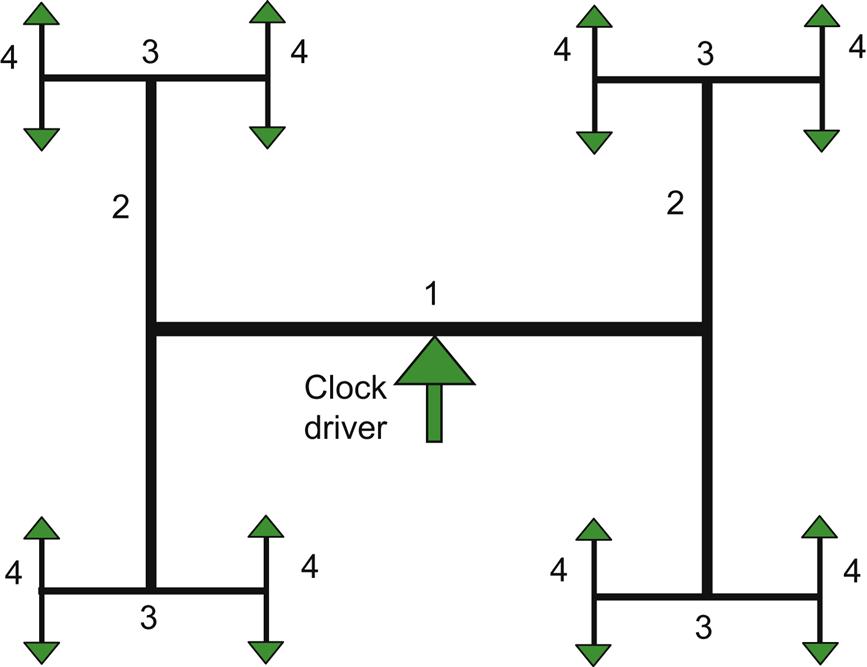
The key concept is to place a mesh within each tier and a global symmetric tree (such as an H-tree) to drive the meshes through TSVs. This dedicated clock tier is placed at the middle of a 3-D stack for the purpose of symmetry, as depicted in Fig. 15.10 for a network spanning four logic tiers. In this configuration, the clock tier is connected to the other tiers from both faces, which means that both face-to-back and face-to-face interconnections are necessary. The intertier interconnects between these two bonding styles are different (e.g., microbumps vs. TSVs), an issue which needs to be considered during the design process.

To assess the performance of this approach, the Alpha 21264 processor has been deployed within a 3-D system [590]. A 2-D floorplan of this processor is split into quadrants, each quadrant placed onto a physical tier, forming a five tier stack including the dedicated clock tier. The cache is split into two tiers and the integer and floating point units are each placed onto two separate tiers. The instruction fetch unit is shared between one of the cache tiers and the tier with the floating point unit. Although this floorplan is rather crude, it offers a reasonable test case for evaluating the performance of a clock tier. The capacitance of each tier is estimated and assigned to each grid unit, where the clock grid has a granularity of Lseg=100 μm. Clock buffers are inserted at intervals of Lbuf=300 μm (see Fig. 15.8).
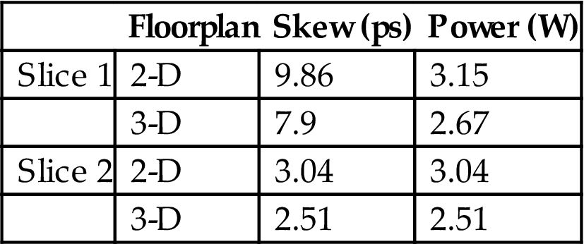
Based on this partition for the planar floorplan of the microprocessor, which is also assumed to be driven by a combined tree and grid network structure, the footprint of the circuit is greatly reduced. More specifically, the area of the clock grid in the 2-D processor is 2.5 mm×2.5 mm, which decreases to 1.25 mm×1.25 mm for the 3-D processor since four tiers are utilized. This decrease in area leads to fewer final stage buffers. The number of these buffers drops from 81 to 25. The buffers drive the grid in all four tiers, which has a total area similar to the 2-D grid since the initial planar floorplan is “folded” to produce the 3-D processor. Consequently, the size of these buffers in a 2-D system is twice as large as a 3-D system. However, as both the total number of buffers and the area of the clock tree driving the grids within the logic tiers have decreased, the power consumption of the clock network has also been reduced. For a 32 nm process node [252], the maximum skew and power consumed by the planar and 3-D system are reported in Table 15.1. The smaller dimensions of the clock network and the fewer buffers decrease both the skew and the power by 15% to 20%.
Table 15.1
Comparison of Clock Skew and Power Dissipation Between 2-D and Four Tier 3-D Microprocessor With Dedicated Clock Tier [589]
| Floorplan | Skew (ps) | Power (W) | |
| Slice 1 | 2-D | 9.86 | 3.15 |
| 3-D | 7.9 | 2.67 | |
| Slice 2 | 2-D | 3.04 | 3.04 |
| 3-D | 2.51 | 2.51 |
The drawback of this global clock distribution network is the requirement for a dedicated tier for the clock circuitry and network. This approach suffers from the same difficulties related to prebond test as the topology shown in Fig. 15.9A. Consequently, a more practical approach would combine a clock tree with a mesh in each tier sharing a common clock source [591]. In Fig. 15.11, the basic elements of a synchronization system for a two tier 3-D circuit is illustrated. An external reference clock is provided prior to bonding the clock generating circuitry. After bonding, a tristate multiplexer in tier 2 disconnects the intratier phase locked loop (PLL) and selects the output from the PLL in tier 1. In this configuration, both networks are driven from a single PLL and are connected at the root of the global tree. The phase detector and DLL in tier 2 ensure that the clock signals within the two tiers are temporally aligned. The clock skew between the two tiers primarily depends upon the process variations and bandwidth of the DLL [591].

An alternative approach that can suppress the additional skew due to process variations increases the number of connections between the clock networks of the two tiers. With this topology, the clock phase alignment circuit can be removed, simplifying the clock circuitry. Furthermore, as several more nodes are shorted between the clock networks, the process variations can be compensated, reducing the overall intertier skew. Interestingly, the power does not decrease, which, in principle, is counterintuitive. This contradictory behavior is due to the use of electrostatic discharge (ESD) diodes for each TSV to protect the driving circuits during manufacturing, which considerably increases the overall power consumption to deliver the clock. Another drawback of this approach is that the physical design of the network is constrained to provide appropriate TSV connections at the shorting nodes.
These topologies have been evaluated on an eDRAM. The test circuit is 5.6 mm×10.9 mm for an IBM 45 nm silicon-on-insulator (SOI) technology [592] and operates at 2.5 GHz. The TSV shorts add a power overhead of only 1%, but the overhead due to the capacitive load of the ESD diodes increases the power consumption by 10% to 30% [591]. Corner analysis has also shown that the approach with shorted grids and typical process corners for both tiers exhibits twice as low a clock skew as compared with the case where the tiers are in different corners (e.g., fast-slow) [591].
These results not only demonstrate the important role of selecting the appropriate number of TSV to manage skew but also show the importance of process variations in 3-D ICs where both intertier and intratier variability must be considered when determining the performance of a 3-D clock network. Due to the importance of this issue, the effects of process and environmental variability on the design of global clock distribution networks are discussed in Chapter 17, Variability Issues in Three-Dimensional ICs.
As a final remark for this section, note that the existing clock synthesis techniques discussed in the following sections have not sufficiently investigated this issue. Consequently, significant effort remains for further improving the present art in 3-D CTS.
15.3 Synthesis of Three-Dimensional Clock Distribution Networks1
Similar to previously discussed techniques, tackling other physical design issues for 3-D circuits such as floorplanning, planar CTS methods have also been adapted to manage the multi-tier nature of these systems and the vertical connections. The majority of 3-D CTS algorithms consist of two primary stages. In the first stage, a suitably modified version of the MMM algorithm, as discussed in Section 15.1, produces a connection topology for the clock sinks located on several tiers. Different variants of this topology generation algorithm have been developed depending upon the target objective(s) of the synthesis technique. In the second stage, another popular technique, DME (also discussed in Section 15.1), is used after appropriate adjustments to embed the 3-D connection topology into a multi-tier stack.
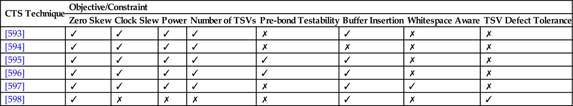
The diversity of 3-D CTS methods can be attributed to the disparate performance objectives as well as the evolution of these methods over the past few years [593–598]. As listed in Table 15.2, 3-D CTS techniques produce clock networks that satisfy a number of objectives in addition to zero (or close to zero) skew and (near-)minimum wirelength. An important objective is lower power consumed by the 3-D clock trees, which, as reported in several works [593–597], entails several tradeoffs among the number of TSVs, wirelength of the 3-D tree, and the TSV capacitance.
Table 15.2
CTS Methods for 3-D Circuits and Related Objectives Satisfied by Each Technique
| CTS Technique | Objective/Constraint | |||||||
| Zero Skew | Clock Slew | Power | Number of TSVs | Pre-bond Testability | Buffer Insertion | Whitespace Aware | TSV Defect Tolerance | |
| [593] | ✓ | ✓ | ✓ | ✓ | ✗ | ✓ | ✗ | ✗ |
| [594] | ✓ | ✓ | ✓ | ✓ | ✗ | ✗ | ✗ | ✗ |
| [595] | ✓ | ✓ | ✓ | ✓ | ✓ | ✓ | ✗ | ✗ |
| [596] | ✓ | ✓ | ✓ | ✓ | ✓ | ✓ | ✗ | ✗ |
| [597] | ✓ | ✓ | ✓ | ✓ | ✗ | ✓ | ✓ | ✗ |
| [598] | ✓ | ✗ | ✗ | ✗ | ✗ | ✓ | ✗ | ✓ |
Considering the global topology and the structures shown in Fig. 15.9, similar tradeoffs have been observed [593,595] where multi-TSV clock trees dissipate, in general, less power than single TSV trees. Limiting the number of TSVs within a 3-D clock tree does not increase power if the TSV capacitance is high, as this capacitive load is counter balanced by the savings due to the lower capacitance of the horizontal interconnects.
Additionally, pre-bond test, which has been shown to be a useful means to improve the yield of 3-D systems [599], requires a different treatment of the clock synthesis process, a situation unique to 3-D systems. To better understand the added complexity of pre-bond testing to the clock synthesis process, consider the example shown in Fig. 15.12 of a two tier clock tree with several sinks and a multi-TSV topology.

The sinks in tier 2 form three disconnected subtrees connected with the subtree in tier 1, forming a 3-D tree connecting all of the 13 sinks. To support pre-bond test for both tiers, a clock tree should exist in either tier and satisfy all of the objectives as compared to a fully connected clock tree of the bonded two tier system. This requirement cannot be satisfied with the illustrated topology unless a redundant network is utilized in tier 2. This redundant network should ensure that the same clock skew and slew are maintained as for the post-bond 3-D tree. In addition, a pre-bond test for tier 1 does not require a redundant tree; however, since the clock loads are different than the full tree, the characteristics of the clock network also differ. Clock synthesis techniques that consider this situation have been developed, where these techniques consider routing and placement obstacles [600] and the placement of TSVs within the available whitespace.
Another issue considered in the CTS process is fault tolerance. As TSVs can suffer from fabrication or assembly defects [601], fault tolerance is an important issue.
The characteristics of several clock synthesis methods are summarized in Table 15.2, where the different objectives addressed by each technique are listed. In the following subsections, techniques with and without pre-bond test are described separately due to the different approaches and resources.
15.3.1 Standard Synthesis Techniques
Classic synthesis techniques for 2-D clock trees are discussed in Section 15.1. These approaches can produce clock trees for 3-D circuits, assuming that each tier contains a tree connecting all of the clock sinks within that tier. The roots of all of these trees are connected through a single vertical connection (e.g., a few TSVs connected in parallel), providing a complete tree spanning the entire 3-D circuit. This single TSV topology, however, is a rather naïve approach as the advantages of the third dimension are not adequately exploited [593]. Consequently, a multi-TSV topology is a superior approach, offering a considerable reduction in wirelength, which typically translates to lower power.
The 3-D clock synthesis problem has been casted in several ways, where the primary objectives are to produce a zero-skew multi-TSV tree with minimum (or near-minimum) wirelength and/or power and the minimum [594] or a bounded number of TSVs [593] for a set of clock sinks ![]() . The clock sinks span several physical tiers. The location of these sinks is described by a triplet of coordinates (xi, yi, zi) where zi indicates the tier of si. In addition, the slew should satisfy a target constraint that is typically less than 5% of the clock period.
. The clock sinks span several physical tiers. The location of these sinks is described by a triplet of coordinates (xi, yi, zi) where zi indicates the tier of si. In addition, the slew should satisfy a target constraint that is typically less than 5% of the clock period.
Techniques for multi-TSV clock tree synthesis proceed in two phases. A topology connecting the clock sinks in all of the tiers of a 3-D system is first generated, followed by an extension of the DME method to embed the topology throughout the tiers of the 3-D system. Topology generation extends the traditional MMM algorithm. As described in Section 15.1, the MMM algorithm operates recursively by bipartitioning a set of clock sinks using an x- or y-cut until only one sink belongs to each set. In 3-D circuits, the clock sinks within a subset produced by a cut are located in different tiers, where those sinks are connected by TSVs. Additionally, a z-cut divides S in several ways, resulting in different demands for TSVs.
The classic MMM algorithm is, therefore, indifferent to TSVs, which can lead to undesirable situations either due to insufficient usage of TSVs to reduce the total wirelength or excessive utilization of TSVs, resulting in lower savings (or even increasing) in power. To address these issues, the MMM algorithm has been extended to control the number of TSVs required by the synthesized tree topologies [593,594].
The MMM-TSV-Bound algorithm, called MMM-TB, generates topologies based on satisfying a user specified upper limit on the number of TSVs. The TSVs are distributed across the area of the tiers [593]. An example of the effect that different bounds of TSVs have on the resulting topologies is shown in Fig. 15.13. As observed in this figure, for larger TSV bounds, additional TSVs are used, where these TSVs appear closer to those sinks connecting a smaller number of internal nodes and/or sinks. This behavior decreases the total wirelength since the horizontal interconnections are shorter. The MMM-TB algorithm begins with a set of sinks S and a TSV bound for each tier within the 3-D system. If stack(S) denotes the number of tiers spanning the sinks of S, at each partitioning iteration, two sets S1 and S2 are produced based on two conditions.

If the TSV bound is one, the existing set S is partitioned to ensure that sinks with the same zi (i.e., from the same tier) are assigned to the same subset. This partition is straightforward as long as stack(S)=2. If, however, the sinks span more than two tiers and since cuts bipartition set S, there are (stack(S)–1) iterations that partition the sinks into the z-direction to ensure that sinks with the same zi are on the same tier. The procedure, illustrated in Fig. 15.14, demonstrates the process in which the partitions in the z-direction occur. In this figure, zmin (zmax) is the lowest (highest) index of the tier that contains the sinks of set S at a specific iteration of the MMM-TB algorithm. In addition, the root of the clock tree is assumed to be located at zr. Indexing the tiers is achieved in ascending order from the bottom tier to the uppermost tier.

As shown in Fig. 15.14, if zr≤zmin, which means the root is located at a lower tier than any of the sinks in S, all sinks with zi=zmin form the (bottom) subset SB and the remaining sinks (e.g., zi∈[zmin+1, zmax]) constitute the (top) subset ST. Alternatively, if zr≥zmax, which means the root is located at a higher tier than any of the sinks in S, all sinks with zi=zmax form the (top) subset ST and the remaining sinks (e.g., zi∈[zmin, zmax−1]) constitute the (bottom) subset SB. In any other case, the (top) subset ST includes those sinks in the same tier as the root of the tree, while the (bottom) subset SB contains the remaining sinks in the other tiers. An example of this procedure for a small set S={a, b, c} is depicted in Fig. 15.15, where the number of TSVs resulting from different z-cuts are illustrated by the thick line segments.

In the second condition, where the TSV bound is greater than one, a cut along the horizontal direction is applied to the median of the x- or y-coordinate of the sinks as in MMM and the z-dimension is not considered. The resulting subsets require several TSVs if sinks with a different z-coordinate are contained in these subsets. At the end of each partitioning step, a new TSV bound is assigned to each subset to ensure that the TSV bound is maintained. This new TSV bound is determined by estimating the number of TSVs required by the newly formed subsets and dividing the bound by the estimated number of TSVs. The TSV estimates are determined from the minimum number of sinks within each tier resulting from the horizontal cuts. The complexity of the MMM-TB algorithm remains the same as that of MMM, which is O(m log m).
The MMM-TB algorithm guarantees that the number of TSVs does not exceed the TSV bound. Any number of TSVs can, however, be employed as long as this bound is satisfied. The number of TSVs greatly affects the total wirelength and, therefore, the power consumed by the clock network. An exhaustive sweep is used to determine the optimum number of TSVs. This approach, however, is computationally expensive, particularly for large TSV bounds. The MMM-TB can be further enhanced to determine the optimal number of TSVs in terms of power. Note that simply using as many TSVs as possible may not yield the least power if the capacitance of the TSVs is high as this trait can adversely affect the savings in power by the decrease in the horizontal wirelength. To determine the number of TSVs, look ahead operations similar to those operations used in [578] are employed [593]. These operations proceed by (a) a z-cut followed by xy-cuts, and (b) xy-cuts followed by a z-cut. The distance of the newly formed centers of mass is compared for cases (a) and (b). A cost function is applied in both cases that relates the resulting number of TSVs and wirelength to estimate the power. The sequence of steps that yields the lower estimate of power is selected during the following iteration.
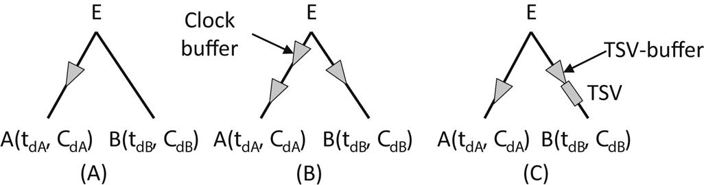
The second phase of the synthesis process is a variant of the DME method, adapted to consider TSVs and a slew constraint. To satisfy slew constraints, a general practice is to not allow the capacitance seen by any node of the tree to exceed a specific limit, Cmax [602]. This constraint is met by adding clock buffers to ensure that the load seen by these buffers remains below Cmax. The merging segments produced from the bottom-up pass of the DME method (see Section 15.1), computed in [593] based on the Elmore delay, are also determined for the buffers whenever the downstream capacitance of the internal nodes exceed Cmax. During the top-down phase, DME is extended to evaluate the type of merging (e.g., merging of an internal node and a buffer from the root of the subtrees or a standard merging of an internal node with the children nodes) and determines the placement of the internal node and buffer. An example of the two different merging types encountered when buffer insertion is integrated with the DME method is illustrated in Fig. 15.16.
Application of the MMM-TB algorithm and the integrated buffer insertion with the DME technique to several benchmarks [603] has demonstrated that multi-TSV clock trees can greatly reduce power, ranging from 16.1% to 18.8%, 10.3% to 13.7%, and 6.6% to 8.3%, as compared to a single TSV clock network where the TSV capacitance is, respectively, 15, 50, and 100 fF, for a two tier circuit. The corresponding decrease in total wirelength is, respectively, 24.0% to 26.5%, 23.9% to 26.6%, and 16.6% to 18.9%. Another advantage of multi-TSV clock trees is that the average slew and distribution of slews are better managed due to the reduced wirelength. Although the combination of the MMM-TB algorithm and the DME method produces efficient multi-TSV clock trees, a greater reduction in wirelength for unbuffered trees is demonstrated by other variants of the MMM and DME methods, which are presented below to offer greater insight.
15.3.1.1 Further reduction of through silicon vias in synthesized clock trees
A simple extension of MMM in three physical dimensions, called MMM-half perimeter wirelength (HPWL), is introduced in [594], where a user defined parameter, ρ (0≤ρ≤1) determines the direction of a cut. If ρ=0, the standard MMM is employed, and the z-dimension is ignored. Alternatively, if ρ=1, the sinks are partitioned among the tiers comprising the 3-D circuit, and the resulting per tier subsets are bipartitioned using xy-cuts as in MMM. For any other ρ, a horizontal cut is performed along the geometric median in a 2-D Manhattan plane. The HPWL for these subsets of sinks is determined. If the HPWL of a subset of sinks is smaller than ρ· HPWL of all of the sinks, the sinks are partitioned among the tiers (i.e., a z-cut) rather than along the xy-directions. This condition shares some concepts with the MMM-TB algorithm, where the TSV bound is used to determine the direction of the sink partition. Furthermore, in the MMM-TB algorithm, constraining the number of TSVs does not guarantee that the total vertical wirelength is minimized.
The MMM-TB algorithm provides the number of TSVs required to connect the sinks during the recursive top-down partition. However, TSV usage also depends upon the tier in which the internal nodes of the connection topology of T(S) are placed. This information, however, is not determined by the MMM-TB algorithm. In addition, the standard DME technique is applied to a 2-D plane where the sinks are projected and does not minimize the number of TSVs.
To demonstrate the different number of TSVs that can originate from diverse placements of the internal nodes of a tree topology, consider the example shown in Fig. 15.17. Depending upon the placement of nodes x1, x2, and the root node sr, the number of TSVs can differ significantly for a two tier tree, as depicted in Fig. 15.17. As illustrated in this example, embedding the nodes for cases (A) and (H) yields the fewest number of TSVs. An algorithm that embeds the tiers to ensure a minimum vertical length is presented in [594]. The vertical length for a 3-D clock tree is
(15.11)
where LTSV is the length of one TSV connecting adjacent tiers, and the summation applies to every pair of nodes within the connection topology of tree T(S). Any pair of nodes placed within the same tier does not contribute to the vertical wirelength since zi=zj. To determine the number of TSVs for a node i of T(S) and, subsequently, the vertical wirelength, the following expressions are used
(15.12a–b)
 (15.12a–b)
where nTSV(Tleft(i)) and nTSV(Tright(i)) are, respectively, the number of TSVs contained in the subtrees rooted at the children of node i and nTSV(i, Tleft(i)) and nTSV(i, Tright(i)) are, respectively, the number of TSVs connecting node i to subtrees Tleft(i) and Tright(i).

If the children of node i are sinks and the location of the sinks is known, the tier(s) where node i can be embedded is notated as ET(i) to ensure that the minimum number of TSVs is determined by the tier of the children nodes. If, however, the children nodes are internal nodes, the embedding tiers for these nodes are sets of embedding tiers. In this case, from these sets of embedding tiers, the set of tiers ET(i) that lead to the minimum number of TSVs nTSV(i) for this node can be determined. An example of embedding an internal node x based on the embedding tiers of the children nodes x1 and x2 is shown in Fig. 15.18. If the children nodes are sinks, which means that x1=s1 and x2=s2, the length of the vertical connection for merging these nodes at node x is |t2−t1|, where t2=z2 and t1=z1 are the tier of the sinks, as depicted in Fig. 15.18A.

If the children nodes are also internal nodes, two cases can be distinguished. If the embedding tiers ET(x1) and ET(x2) have some common tier(s), the minimum vertical length to merge these nodes with node x is nTSV(Tleft(x))+nTSV(Tright(x)), and the tier where the node is embedded is between tier t2 and t3, as shown in Fig. 15.18C. Choosing any other tier for embedding x results in an increase in nTSV(x), as depicted in Fig. 15.18D. In the second case, where the set of embedding tier(s) for the children nodes x1 and x2 do not share any common embedding tier, as shown in Fig. 15.18E, node x is embedded between tier t2 and t3. The difference between these two cases, as shown in Figs. 15.18C and 15.18E, a common embedding tier for the children nodes exists in Fig. 15.18C and, consequently, merging with node x does not require a TSV. As shown in Fig. 15.18E, however, |t3−t2|>1 and at least one TSV is required to embed node x.
The set of embedding tiers for the internal nodes (required by (15.12a)) is iteratively determined in a bottom-up process [594],
(15.13)
where
(15.14)
and
(15.15)
The optimality of these expressions has been proven through a series of lemmas [594]. The process of embedding the nodes of a tree to ensure that the minimum vertical length is employed exhibits a complexity of O(m) where m is the number of nodes of tree T(S).
Once the embedding tiers for the nodes within a tree are determined, the placement of the nodes of the tree follows based on the DME technique, where the Elmore or a linear delay model is employed. In a linear delay model, the TSVs are modeled differently due to a disimilar capacitance as compared to the horizontal wires. As with the application of DME to 2-D clock trees with a linear delay model, zero skew with minimum wirelength is also produced for 3-D clock trees. The situation is more subtle since the Elmore delay is used for ea and eb for merging nodes a and b (see Section 15.1). This approach can lead to a suboptimal wirelength due to the lack of a specific position along a merging segment to balance the delay from the merging node x to the root of subtrees Ta and Tb. This behavior requires wire snaking, which results in detouring from the minimum wirelength.
15.3.2 Synthesis Techniques for Pre-bond Testable Three-Dimensional Clock Trees
The previously discussed synthesis techniques produce 3-D clock trees for any number of tiers, yet suffer from a drawback that limits usability. As pre-bond test can guarantee high yield of 3-D systems [604], the correct functionality and expected performance of each tier should be verified prior to assembly of the stack. This demand places considerable constraints on the design of 3-D systems. For pre-bond test methodologies of 3-D circuits, see [605]. For the design of clock trees, specific changes must be made to provide pre-bond test. The fundamental difference of pre-bond test related to CTS techniques is the additional circuitry. The salient features of these techniques are presented in this section.
A method for providing a 3-D clock distribution network that can be tested during pre-bond is to utilize single TSV topologies as shown, for example, in Fig. 15.19, where these topologies include fully connected trees in each tier of the 3-D system. One clock input for each tier provides the clock signal to all of the clock pins within that tier. This approach, however, yields minor improvements over 2-D circuits, reducing the advantages of 3-D integration. Instead, adapting multi-TSV clock networks to support pre-bond test is more advantageous. The main challenge is in multi-TSV topologies. There is typically only one tier that contains a fully connected tree (typically the tier where the primary clock driver resides), while the other tiers comprise several (or a forest) of trees connected to the full tree through TSVs. These several trees within each tier are however disconnected from each other during pre-bond test operation. A non-negligible number of clock inputs is required to clock these disconnected trees prior to bonding, complicating the test process and increasing cost.

Additionally, even for the tier that includes the fully connected clock network, test is not a simple process as this network drives the entire clock load. During pre-bond test, only part of this load exists, which means that clock skew and slew can deviate significantly from the target skew and slew during normal operation. This network can, therefore, cause several timing violations that can incorrectly be interpreted as faults. To mitigate this situation, two measures are applied: (1) insert a buffer at each node of the complete network that connects to a TSV, and (2) add an appropriate number of redundant networks that connect the local trees of a tier with each other during pre-bond test. During normal operation, that is post-bond, these redundant trees are disconnected from the rest of the clock network [606]. Buffer insertion from (1) decouples the fully connected tree from the rest of the network. Consequently, the capacitance at each node of this clock tree remains the same during both pre- and post-bond operation.
An example of a pre-bond testable clock tree in two tiers is shown in Fig. 15.20. Drawn with dashed lines, the buffers before the TSVs, the redundant tree, and the transmission gates (TGs) that disconnect this tree during normal operation, are noted in this figure. Also note that an additional control signal is required for this structure to switch the TGs in tier 2.

Having described the characteristics of pre-bond testable clock networks, the synthesis problem is formulated as follows: for a set of sinks ![]() distributed across n tiers, a root node sr, and a TSV bound, synthesize a 3-D clock network with a minimum or zero clock skew both in post-bond (for the entire stack) and pre-bond (for each tier) operation. The wirelength and power of the 3-D clock network are minimized while simultaneously satisfying the clock slew constraints.
distributed across n tiers, a root node sr, and a TSV bound, synthesize a 3-D clock network with a minimum or zero clock skew both in post-bond (for the entire stack) and pre-bond (for each tier) operation. The wirelength and power of the 3-D clock network are minimized while simultaneously satisfying the clock slew constraints.
Employing the MMM-TB method, as described in the previous section, a connection topology for the sinks of S, denoted as T(S), is generated. The MMM-TB method produces a topology where the sinks are located on the same tier as the source, called herein the source tier. These sinks are connected by a tree. Connections to other tiers are implemented with TSVs. To decouple the subtrees in these tiers from the network in the source tier, the following steps are followed [596]: (1) if a TSV connects the source tier with another tier, a TSV buffer is inserted in the source tier, (2) if two nodes of the 3-D clock tree are connected by a TSV traversing the source tier, a TSV buffer is added to the source tier, and (3) if one TSV interconnects two nodes without traversing the source tier, no TSV buffer is inserted. In this case, the absence of this TSV during pre-bond test has no effect on the capacitance of the source tier and, therefore, a TSV buffer is not needed.
The next phase of the synthesis process includes a modified DME, which is a two stage technique. In this pre-bond aware CTS (PBA-CTS) technique, a zero skew tree is produced that considers merging segments both for the TSV buffers and the nodes of the connection topology originating from the MMM-TB algorithm. The TSV buffers, however, often require additional wirelength to maintain the zero (or low) skew requirement [596]. This situation can result in the minimum wirelength objective to not be satisfied. The insertion of common clock buffers avoids this situation. Consider the example shown in Fig. 15.21 where two subtrees, ST1 and ST2, are, respectively, in tiers one and two. A TSV buffer is used to merge these subtrees as the trees are located on separate tiers. This TSV buffer adds to the delay from node E to ST2. If this delay is much greater than the delay from E to ST1, before the insertion of the TSV buffer, this delay increases. Wire “snaking” is added to maintain the zero skew objective, which departs from the minimum wirelength objective. A clock buffer can be inserted to avoid wire snaking. Case studies show that these imbalances occur infrequently; the use of a clock buffer for this purpose is, therefore, not a significant issue.

Another reason exists for adding clock buffers during the bottom-up process where the merging of subtrees takes place. Clock buffers are widely used to satisfy slew constraints. Inserting these clock buffers ensures that the load that each clock buffer drives does not exceed a downstream capacitance threshold Cmax [602]. This practice has been shown to control slew. In the case of pre-bond testable 3-D clock trees, examples where the clock and TSV buffers are inserted are illustrated in Fig. 15.22. The simple case is shown in Fig. 15.22A, which is common in both 2-D and 3-D (either pre-bond testable or not) synthesized clock trees if the delay of the merged branches is highly imbalanced (e.g., tdA<tdB). In Fig. 15.22B, multiple clock buffers are utilized due to the excessive length of the wires and/or if the downstream capacitance exceeds Cmax. Another case is shown in Fig. 15.22C, which requires the addition of a clock buffer to counteract the delay imbalance caused by inserting a TSV buffer. The insertion of the TSV buffer also decouples the subtrees, thereby facilitating pre-bond test.
The output of the PBA-CTS method is a 3-D clock tree used for post-bond operation and a tree that spans all of the clock sinks lying in the source tier. Similar trees are generated for the remaining tiers, which is achieved by redundant trees connecting the unconnected trees in these tiers. This process is similar to a conventional CTS technique for planar circuits [596] comprising: (1) construction of a binary connection topology T(S) generated in a top-down manner, (2) insertion of a TG at each sink node, and (3) embedding and buffering of T(S) in a tier under skew and minimum wirelength constraints. Note that the sinks are the roots of the subtrees connected by the redundant tree in this tier. Insertion of the TGs, which connect (pre-bond operation) or disconnect (post-bond operation) the redundant tree, requires a control signal spanning a large portion of the tier. To limit the wirelength of this signal, the rectilinear minimum spanning tree (RMST) algorithm can be used [403,607].
IBM [603] and ISPD [608] benchmark circuits are utilized to ascertain the efficiency of this pre-bond CTS technique, where the clock sinks are randomly assigned within the tiers of the 3-D circuits. A 45 nm process node based on the Predictive Technology Model (PTM) model is assumed [252]. The clock frequency is 1 GHz and the power supply is 1.2 volts. A via-last TSV technology is used where the area, length, and liner thickness of a TSV are, respectively, 10 μm×10 μm, 20 μm, and 0.1 μm. The clock skew and slew constraints are, respectively, 10% and 3% of the clock period. Other electrical and physical characteristics assumed for these circuits are listed in [596]. A comparison of a single TSV, which is inherently pre-bond testable, and multi-TSV clock trees, which require redundant trees and TSV buffers, has demonstrated that multi-TSV clock trees decrease wirelength from 14.8% to 24.4% and 39.2% to 42.0%, for circuits with, respectively, two and four tiers. The savings in power vary from 10.1% to 15.9% and from 18.2% to 29.7%, respectively, for circuits comprising two and four tiers.
The departure between the wirelength and power savings, as wirelength and power depend linearly on wire capacitance, is attributed to the additional circuits, such as the TSV buffers and TGs, and the TSV capacitance, which can be greater than the capacitance of the horizontal wires on a per unit length basis. Furthermore, the control signal for the TGs adds to the overall wirelength congestion of the clock trees. The breakdown of the wirelength components for several benchmark circuits implemented in two tiers is reported in Table 15.3. The wirelength breakdown is reported for the post-bond 3-D clock trees, the pre-bond trees in the source tier (tier 1), and the pre-bond trees in tier 2. Notably, the length of the control signal of the TGs constitutes a significant portion of the total wirelength (on average, 29%).
Table 15.3
Post-bond Testable 3-D Clock Trees and Pre-bond Testable 2-D Clock Trees of the Individual Tiers for a Two Tier 3-D Circuit [596]
| Circuit | # of Sinks | # of TSVs | Post-bond 3-D | Pre-bond Testable Tier 1 | Pre-bond Testable Tier 2 | |||||||||
| Wirelength (μm) | Power (mW) | Skew (ps) | Wirelength (μm) | Power (mW) | Skew (ps) | Wirelength (μm) | Power (mW) | Skew (ps) | ||||||
| Total | Subtrees | Redundant | TG Control Signal | |||||||||||
| r1 | 267 | 57 | 227,141 | 128.4 | 13.7 | 166,691 | 103.0 | 13.5 | 150,219 | 60,450 | 89,769 | 62,732 | 68.2 | 13.0 |
| r2 | 598 | 95 | 488,987 | 274.1 | 14.2 | 328,914 | 196.0 | 14.1 | 302,023 | 160,073 | 141,950 | 109,031 | 148.6 | 11.8 |
| r3 | 862 | 183 | 616,077 | 361.6 | 15.5 | 444,156 | 280.5 | 15.5 | 429,950 | 171,921 | 258,029 | 161,561 | 201.9 | 16.2 |
| r4 | 1903 | 265 | 1,311,290 | 763.2 | 15.5 | 889,460 | 536.4 | 14.9 | 846,980 | 421,830 | 425,151 | 259,442 | 422.1 | 15.1 |
| r5 | 3101 | 269 | 1,998,950 | 1115.0 | 29.1 | 1,255,760 | 715.9 | 29.1 | 1,236,417 | 743,190 | 493,227 | 310,885 | 615.9 | 20.9 |
| f11 | 121 | 44 | 129,391 | 73.3 | 9.4 | 99,393 | 64.1 | 9.2 | 99,169 | 29,998 | 69,171 | 51,214 | 44.3 | 6.3 |
| f12 | 117 | 36 | 127,763 | 71.2 | 6.8 | 96,093 | 60.4 | 6.2 | 93,625 | 31,669 | 61,956 | 42,134 | 42.0 | 5.7 |
| f21 | 117 | 42 | 136,676 | 75.6 | 5.0 | 107,834 | 67.0 | 4.7 | 101,968 | 28,841 | 73,127 | 52,241 | 45.0 | 7.3 |
| f22 | 91 | 30 | 80,977 | 46.8 | 15.3 | 61,504 | 40.4 | 15.2 | 59,870 | 19,473 | 40,397 | 29,449 | 26.4 | 14.9 |
| Ratio | 1.00 | 1.00 | 1.00 | 0.72 | 0.79 | 0.97 | 0.69 | 0.28 | 0.41 | 0.29 | 0.57 | 0.94 | ||

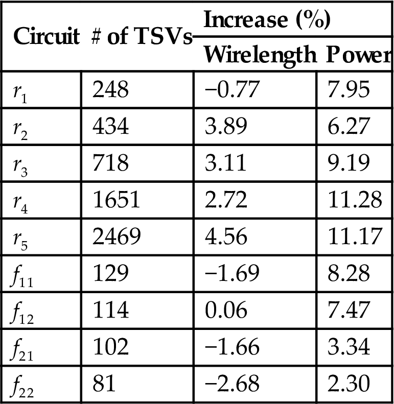
Another potential source of overhead is the TSV buffers. The change in wirelength and power from the case where no TSV buffers are used in the source tier to decouple that tree from the downstream capacitance in the other tiers is listed in Table 15.4. The change in wirelength is small; for specific benchmark circuits, a decrease in the interconnect length is observed. Alternatively, an increase in power is always observed, verifying that inserting TSV buffers narrows the power gains for multi-TSV clock trees that are pre-bond testable.
Table 15.4
TSV Buffer Insertion on Wirelength and Power [596]
| Circuit | # of TSVs | Increase (%) | |
| Wirelength | Power | ||
| r1 | 248 | −0.77 | 7.95 |
| r2 | 434 | 3.89 | 6.27 |
| r3 | 718 | 3.11 | 9.19 |
| r4 | 1651 | 2.72 | 11.28 |
| r5 | 2469 | 4.56 | 11.17 |
| f11 | 129 | −1.69 | 8.28 |
| f12 | 114 | 0.06 | 7.47 |
| f21 | 102 | −1.66 | 3.34 |
| f22 | 81 | −2.68 | 2.30 |
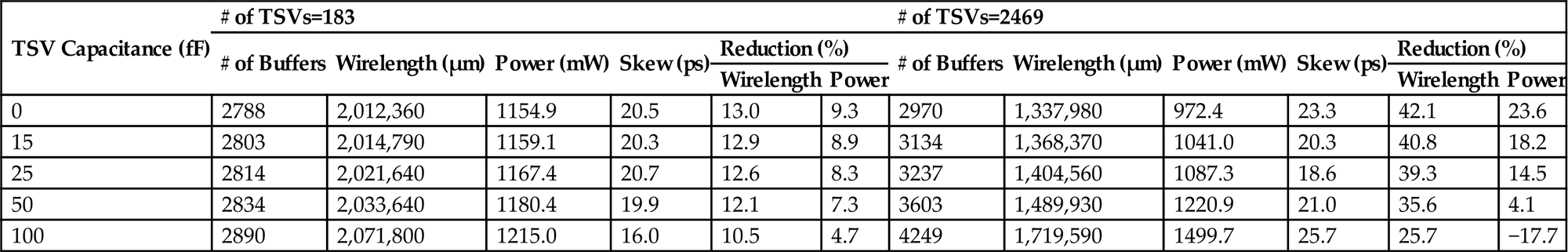
Lastly, the effect of the TSV capacitance on the performance of a 3-D clock trees is assessed by the results reported in Table 15.5 for the IBM benchmark circuit r5. These results include disparate TSV bounds, which constrain the number of TSVs in the clock tree. Two interesting observations are noted from these results. First, the power worsens with increasing TSV capacitance irrespective of the TSV bound. Second, increasing the TSV bound lowers power as more TSVs drive a shorter interconnect length. This trend is reversed if the TSV capacitance is much larger, increasing the power by 17.7% for 2,469 TSVs and a TSV capacitance of 100 fF.
Table 15.5
TSV Capacitance and TSV Bound for Different Metrics as Compared to Single TSV Clock Trees [596]
| TSV Capacitance (fF) | # of TSVs=183 | # of TSVs=2469 | ||||||||||
| # of Buffers | Wirelength (μm) | Power (mW) | Skew (ps) | Reduction (%) | # of Buffers | Wirelength (μm) | Power (mW) | Skew (ps) | Reduction (%) | |||
| Wirelength | Power | Wirelength | Power | |||||||||
| 0 | 2788 | 2,012,360 | 1154.9 | 20.5 | 13.0 | 9.3 | 2970 | 1,337,980 | 972.4 | 23.3 | 42.1 | 23.6 |
| 15 | 2803 | 2,014,790 | 1159.1 | 20.3 | 12.9 | 8.9 | 3134 | 1,368,370 | 1041.0 | 20.3 | 40.8 | 18.2 |
| 25 | 2814 | 2,021,640 | 1167.4 | 20.7 | 12.6 | 8.3 | 3237 | 1,404,560 | 1087.3 | 18.6 | 39.3 | 14.5 |
| 50 | 2834 | 2,033,640 | 1180.4 | 19.9 | 12.1 | 7.3 | 3603 | 1,489,930 | 1220.9 | 21.0 | 35.6 | 4.1 |
| 100 | 2890 | 2,071,800 | 1215.0 | 16.0 | 10.5 | 4.7 | 4249 | 1,719,590 | 1499.7 | 25.7 | 25.7 | −17.7 |
Although the results listed in Tables 15.3 to 15.5 demonstrate considerable improvements, two limitations of the CTS technique in [596] are noted. One of these limitations relates to the effect of the added TSV buffers, which can produce delay imbalances that are controlled by additional clock buffers. The outcome is increased power. Another limitation stems from the use of TGs in all but the source tier to (dis)connect the redundant trees according to the operational mode (pre- or postbond). Indeed, as listed in column 13 of Table 15.3, the interconnect overhead due to the control signal of the TGs (although the routing of this signal is embedded with RMST) reaches, on average, 29% of the total wirelength of the post-bond clock tree. This overhead adds to the wirelength required by the clock distribution network or, alternatively, severely curtails the benefits of pre-bond testable multi-TSV trees.
These limitations can be circumvented through more elaborate CTS methods and a suitable self-configured circuit that can substitute for the TGs [595]. This approach commences with an advanced methodology for topology generation, called herein MMM-HPWLmax, which is based on the MMM-HPWL algorithm followed by the embedding of the topology in the tiers of the stack to minimize the vertical wirelength [594]. These steps provide a post-bond 3-D clock tree. To generate the redundant clock trees for pre-bond test, the same methods are applied again to all but the source tier, where the TGs are replaced by a self-configured circuit that adapts to the operating mode.
There are two primary differences between this method, called herein low overhead pre-bond aware CTS (LO-PBA-CTS) [595], and PBA-CTS [596]. These differences are (1) relaxation of the constraint that a buffer should be placed before a TSV to decouple the tree in the source tier from the downstream subtrees, and (2) elimination of the control signal for the TGs along with the associated interconnect overhead.
Consequently, in LO-PBA-CTS, a buffer can be placed anywhere along the branch of the tree that connects to a TSV. Greater flexibility is, therefore, offered for placing the buffers, lowering the likelihood of inserting a TSV buffer that produces a delay imbalance during the node merging process. This flexibility may, however, be insufficient to prevent delay imbalances, in particular when a TSV buffer is inserted at a branch with a small capacitive load. To cope with this situation, the TSV buffers are characterized as stable or unstable [595]. A TSV buffer is stable if inserting this buffer isolates the tree of the source tier and does not require insertion of another clock buffer at another edge to satisfy delay imbalances. Otherwise, a TSV buffer is unstable.
The LO-PBA-CTS technique manages the unstable TSV buffers through the MMM-HPWLmax algorithm [594], which builds on the MMM-HPWL. Whereas the latter algorithm handles the density of TSVs by the parameter ρ during the recursive bipartition, the MMM-HPWLmax checks whether the HPWL of the sinks included in a candidate subset is less than or equal to HPWLmax,cap,
(15.16)
where Cmax is the maximum capacitance constraint, cw is the unit length capacitance of the horizontal interconnects, and Cmax,sink is the maximum capacitive load of all of the sinks. MMM-HPWLmax employs the threshold max(HPWLmax,cap, ρ·HPWL) to decide whether partitioning the sinks occurs in the z-direction or along the xy-directions. This threshold is rather conservative as the TSV capacitance is not included; however, simulation results demonstrate that the number of unstable TSV buffers is reduced, particularly in those circuits with a high number of clock sinks [595]. Note that this treatment resembles the practice of [596] to satisfy slew constraints but targets a different design objective.
The other key difference of LO-PBA-CTS [595] as compared to PBA-CTS [596] is the use of a self-configured circuit to switch the TGs connecting the redundant clock tree in all but the source tier. This circuit is depicted in Fig. 15.23, where, in addition to the TG, only a handful of transistors are required. The circuit operates as follows. During pre-bond test, the clock signal is supplied to the root of the redundant tree and reaches the root of every subtree preceded by a TG. A rising edge of the clock signal Tclk is inverted by INV1 and the device P2 turns on, charging node PBTEST to Vdd. This high voltage drives the output of INV3 low, turning off N2. The output signal of inverters INV3 and INV4 produces the control signals for the TG.
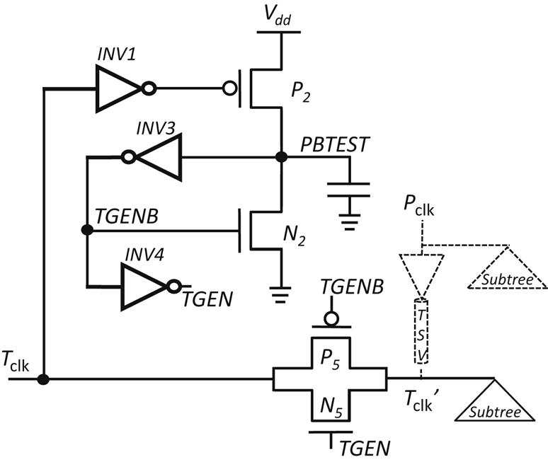
Alternatively, if the Tclk signal is low (no pre-bond test), P2 turns off. The capacitance of node PBTEST slowly discharges through the different leakage current paths. At some time, the output of INV3 is driven high, turning on N2, completely discharging node PBTEST. The TG is also turned off, disconnecting the redundant tree. The turn-off time of the circuit can be regulated by sizing P2 and N2, which are along, respectively, the charge and discharge paths of node PBTEST. The circuit in [595] is based on a 45 nm predictive technology [252], resulting in a turn-off time of about 100 ns.
Application of LO-PBA-CTS to the same benchmark circuits as in PBA-CTS and the same technology parameters demonstrates comparable results in terms of wirelength, clock skew, slew rate, and power. However, for specific benchmark circuits, such as ispd09fnb1 and ispd09fnb2, reductions of 56% to 88% in the number of TSVs, 53% to 67% in the number of buffers, 22% to 65% in total wirelength, and 26% to 43% in the power of the post-bond clock distribution network are observed. Additionally, the wirelength overhead of the control signal for the TGs no longer exists. Further developments in CTS techniques for 3-D clock trees emphasize other important issues, such as limitations on the TSV placement. These techniques are reviewed in the following section.
15.4 Practical Considerations of Three-Dimensional Clock Tree Synthesis
The methods presented in Section 15.3 have significantly advanced the state-of-the-art for 3-D CTS. More recent approaches have enhanced the efficiency of these techniques by considering more practical issues, such as whitespace availability and obstacle avoidance for the TSVs (which can affect important metrics, such as clock skew, slew rate, wirelength, and power) as well as fault tolerance.
The majority of the physical design techniques reviewed in Chapter 9, Physical Design Techniques for Three-Dimensional ICs, highlight the importance of whitespace in 3-D circuits where TSVs and buffers (or repeaters) are inserted. Due to the nature of TSVs, which disrupt cell placement, the placement of the clock signal TSVs can also affect the whitespace. An approach to address this practical constraint is, after applying one of the techniques discussed in Section 15.3, to shift the TSVs to the nearest available whitespace. This approach is illustrated in Fig. 15.24, where the dashed lines depict the additional wire segment. This shift of the TSV location can negate the (near-)optimality of the DME technique (and its variants), degrading the performance of the synthesized clock network.

Considering the constraints in placement due to the whitespace, the clock synthesis problem can be formulated as follows. For a target whitespace area (fragmented into several parts, the number and size of which depends upon the floorplan parameters, see Chapter 9, Physical Design Techniques for Three-Dimensional ICs) within each tier, a set of clock sinks S, a bound for the number of TSVs, and a slew constraint, synthesize a clock tree to ensure that (1) the number of TSVs does not exceed the TSV bound, (2) each TSV is placed within some whitespace, (3) the clock slew constraint is met, and (4) clock skew and power are minimized.
To address this problem, a three-stage method is employed [597], where these stages include: (1) pre-clustering of sinks, (2) an extension of the MMM-TB method to consider available whitespace, and (3) the application of the DME technique to place the TSVs within the whitespace. The computational complexity of this method is O(kwsm), where kws is the number of whitespace blocks and m is the number of clock sinks in S.
The pre-clustering step proceeds by clustering all of the clock sinks located within a specific radius from each whitespace and assigning these sinks to the corresponding whitespace. The whitespace from all of the tiers is projected onto a single plane, forming a set of whitespace regions. A parameter β controls the assignment of a sink to a whitespace. For sinks situated farther than β⋅HPWLtier (HPWLtier is the HPWL of the tier) from the nearest whitespace, these sinks are clustered. This clustering means that a TSV placed in a nearby whitespace provides the clock signal to all of the sinks. To comply with the design requirements for a clock network, each cluster is treated as a subtree, the root of which is contained within a whitespace. An example of sink clustering is shown in Fig. 15.25. The traditional MMM and DME methods produce a tree connecting these sinks to the corresponding whitespace. Consequently, at the end of this stage, a new set of sinks is formed that also includes the root of these subtrees. The downstream capacitance of the roots and the delay to the sinks is, respectively, the input delay and capacitive load for these root nodes in the two successive stages of the technique. Furthermore, the clustered sinks are removed from set S.

The second stage is based on the MMM-TB algorithm (see Fig. 15.14), where the decision of the direction of bipartition also considers the whitespace. Assume that at an iteration of the algorithm, two subsets with sinks SA and SB result from xy-cuts. If the sinks contained in these subsets are only placed within one tier, meaning that stack(SA)=1 and stack(SB)=1, no TSVs are needed and no whitespace is required to proceed with the partition. Alternatively, if stack(SA)>1 and stack(SB)>1, whitespace exists in all of the stack(SA)−1 and stack(SB)−1 tiers to ensure that the TSVs can be inserted to connect the sinks of these subsets. Otherwise, the xy-cut does not occur and the partition occurs in the z-direction (see Fig. 15.14). Generation of this connection topology that is also whitespace aware completes the second stage.
A variant of DME is employed during the last stage to produce the clock tree. During the bottom-up phase of this stage, the merging segments for all of the nodes are generated, including the nodes related to a TSV, where these nodes are placed within the whitespace. As the whitespace can contain multiple clock TSVs, crosstalk noise can develop among these TSVs. This issue emerges if the physically adjacent TSVs within some whitespace carry the clock signal at a different hierarchical level of the clock network. The latency of the clock signal from the root to these TSVs can differ. The signal transferred by these TSVs can, therefore, be out-of-phase, increasing coupling within the clock network. To alleviate this noise, modifications of the merging segments of the nodes with TSVs are relocated to the center of the nearest whitespace. The location of the TSV may be farther from this whitespace.
An example of this diversion from the initial merging segment is shown in Fig. 15.26. The whitespace is divided into several squares. The size of this space is determined by the area of a single TSV and the TSV keep-out zone. Any square that overlaps with the merging segment of that TSV is an appropriate location. If, however, this placement leads to coupling with neighboring TSVs, a more distant square is used, and wire “snaking” is required to cope with the delay imbalance. Note that as individual TSVs are placed, suboptimal placements are produced. To satisfy slew constraints, buffer insertion as in the PBA-CTS technique is applied but as a post-synthesis step.

The efficiency of this technique is evaluated on ISPD benchmark circuits for a two tier system assuming a 45 nm CMOS technology node [252]. The clock sinks and whitespace are randomly distributed across the two tiers. The clock frequency is 2 GHz and the power supply is 1.2 volts. The clock slew constraint is 100 ps. A comparison between the whitespace aware method and a clock synthesis method consisting of the MMM-TB, DME, and buffer insertion is performed for different scenarios. These results are listed in Table 15.6, where the number and area of the whitespace as a per cent of the tier area are listed in the first column of the table.
Table 15.6
Effect of Whitespace Area on the Number of TSVs, Skew, Power, and Slew on Different Whitespace Aware and Unaware Methods, where the Bound for TSVs is 20 [597]
| Whitespace No/Area (%) | MMM-TB, DME, Buffer Insertion, W/O TSV Relocation | MMM-TB, DME, Buffer Insertion, After TSV Relocation | Whitespace Aware CTS [597] | |||||||||
| # of TSVs | Skew (ps) | Power (W) | Slew Violation | # of TSVs | Skew (ps) | Power (W) | Slew Violation | # of TSVs | Skew (ps) | Power (W) | Slew Violation | |
| 4 (4.11) | 20 | 23.81 | 0.299 | No | 20 | 175.78 | 0.358 | Yes | 2 | 28.58 | 0.294 | No |
| 9 (5.64) | 20 | 23.81 | 0.299 | No | 20 | 148.98 | 0.336 | Yes | 9 | 41.28 | 0.314 | No |
| 16 (10.03) | 20 | 23.81 | 0.299 | No | 20 | 55.14 | 0.314 | No | 14 | 40.09 | 0.308 | No |
| 29 (12.86) | 20 | 23.81 | 0.299 | No | 20 | 83.06 | 0.309 | No | 18 | 32.45 | 0.309 | No |
| 36 (14.47) | 20 | 23.81 | 0.299 | No | 20 | 40.94 | 0.304 | No | 19 | 26.41 | 0.310 | No |
| 55 (16.23) | 20 | 23.81 | 0.299 | No | 20 | 33.22 | 0.302 | No | 20 | 32.01 | 0.302 | No |
| 131 (19.79) | 20 | 23.81 | 0.299 | No | 20 | 22.98 | 0.301 | No | 20 | 25.33 | 0.302 | No |
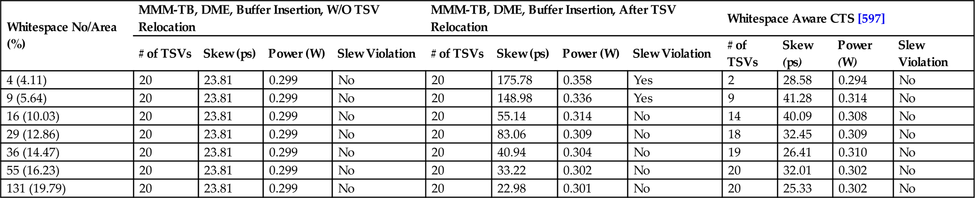
Columns 6 to 9 correspond to those results after the TSVs are moved into the nearest whitespace. This practice, however, leads to slew violations, most likely due to an increase in the capacitance of the path after the TSV is relocated. Furthermore, the whitespace aware method seems to utilize fewer TSVs than the TSV bound (which, in this case, is 20). The rationale behind this behavior is that if fewer and smaller whitespaces exist, the extension of the MMM-TB method to produce the connection topology discourages xy-cuts that produce several TSVs since no whitespace (at least at a reasonable distance) is available to accommodate these TSVs. This lack of whitespaces exacerbates the clock skew reported in column 7, as relocating the TSVs adds significant wirelength. As the number and area of the whitespace blocks increase, however, the performance of the different methods deviates less. This result is due to less of an effect of the post-synthesis TSV relocation process than for whitespace unaware methods due to the greater availability of whitespace.
Another practical issue that has drawn attention in CTS is the presence of defects in TSVs, which can render a 3-D stack inoperable [604]. Due to the criticality of the clock networks, adding fault tolerance to a 3-D clock network is a reasonable objective. The simplest way to achieve this objective is TSV redundancy. Two or more TSVs can be utilized for each intertier connection within a clock network. The area (and power) overhead is, however, significant. Consequently, more advanced redundancy schemes have been proposed [609–612]. Some of these schemes are depicted in Fig. 15.27. The method of double (or higher) redundancy, shown in Fig. 15.27A, replicates the number of TSVs. To reduce the area overhead, for example, the 4:2 topology illustrated in Fig. 15.27B uses multiplexers to reroute the signal transferred by a defective TSV to a spare TSV. This rerouting can add significantly to the delay of a signal. In Fig. 15.27C, in the 4:1 topology, a signal is shared between two adjacent TSVs through multiplexers, where the signal to a defective TSV is shifted to a neighboring connection. A spare TSV is used, thereby tolerating a single defect. The last scheme shown in Fig. 15.27D includes no spare TSVs and shares a signal with three TSVs, which enhances the ability to tolerate TSV faults.
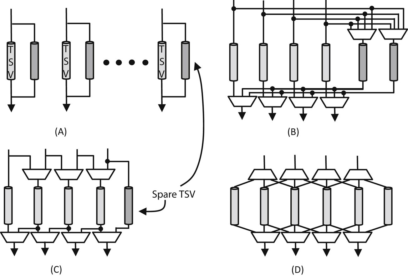
Introducing these defect tolerance mechanisms to a clock network is feasible but the overhead in area and power can be prohibitive. An approach that requires less overhead utilizes existing TSVs within the clock network. These TSVs are inserted by the CTS technique to tolerate faults from defective TSVs. The key concept of this approach is a TSV fault tolerant component (TFC). The operation of TFC is described in Fig. 15.28. As shown in this figure, additional circuitry is needed. This circuitry includes one TG (i.e., TGT) and multiplexers, MUX1 and MUX2, while the other TGs are available from the pre-bond testable clock network. These TGs connect the redundant clock tree during pre-bond test. This scheme exhibits a lower overhead as compared to the schemes depicted in Fig. 15.27.

The essence of this technique is to form pairs of existing TSVs and use these pairs to form TFCs, which operate as follows. If the tiers are not bonded, pre-bond operation is achieved by enabling the TGs to connect the redundant clock tree and supply the clock signal across a tier. During post-bond operation without any TSV defects, all of the TGs are off and the clock signal propagates through “healthy” TSVs. If any of the two TSVs is defective, the TGs and multiplexers are configured to ensure that the clock signal delivered from the healthy TSV is propagated to another subtree through the wire segment connected by TG1 and TG2. This scheme can be further extended to include more TSVs, offering enhanced fault tolerance. The complexity and associated overheads, however, make the usage of pairs or triplets of TFCs more beneficial [598].
This method is applied as a post-synthesis technique, and should, therefore, be placed to not degrade the characteristics of the synthesized clock tree. Pairs of TSVs can form a TFC whenever a TSV is added. First, a check is performed to determine whether other TSVs are located within a radius rp from the placed TSV, as illustrated in Fig. 15.29. If several TSVs exist, the closest TSV is chosen to form a pair, yielding a TFC. If only TSVs that belong to other TFCs exist, the recently placed TSV can be used to form a triple TFC. If this possibility does not exist or if no TSVs are within the specified distance, double redundancy is employed to provide defect tolerance. A crucial component in forming a TFC is the radius rp, which is determined from the TSV characteristics and the fabrication technology [598].

This fault tolerance scheme has been applied to several synthesized 3-D clock trees [580], where two tiers comprise the 3-D stack. A comparison among three fault tolerant techniques, double redundancy, only pair TFCs, and both pair and triple TFCs, is performed using an industrial circuit with 55.4 clock sinks. This comparison demonstrates that the pair and triple TFCs reduce the area overhead as compared to double redundancy by, respectively, 40% and 58%. The power overhead due to the use of pair and triple TFCs as compared to a clock network without fault tolerance is, respectively, 29% and 32%. The additional improvement in yield offered by the TFCs as compared to double redundancy is 1.27%, while the increase in skew and wirelength does not exceed 3%. Consequently, using the existing resources of the clock network, defect tolerance can be provided with moderate overhead.
15.5 Summary
CTS techniques and global clock distribution networks for 3-D circuits are reviewed in this chapter. The majority of 3-D CTS methods are based on standard CTS methods, such as the method of MMM and the DME method. The primary enhancements, differences, and traits of 3-D CTS approaches and global clock network topologies are summarized as follows:
• Symmetric planar topologies have been extended to three dimensions, where a different number of TSVs is required to provide the clock signal to all of the tiers within a 3-D circuit. Single and multi-TSV global networks have been proposed, where the number of TSVs is traded off with power and wirelength.
• Multi-TSV topologies do not inherently support pre-bond test and, therefore, require redundant trees during pre-bond test.
• A clock network that combines in each tier a global tree with a grid is more robust to process and environmental variations, typically at the cost of increased power. The meshes can be shorted at several points through TSVs to lower intertier variations.
• A dedicated tier that includes the global clock network and related clock circuitry supports individual optimization of the clock delivery topology and circuitry. The other tiers comprise the logic and memory of the system. Each tier, except for the clock tier, includes a mesh to provide the clock signal to the clock pins in these other tiers.
• 3-D CTS techniques usually proceed in two phases. A top-down phase to generate a connection topology for a set of clock sinks, and a second phase where the generated topology is embedded into the tiers of the 3-D circuit.
• The top-down phase is based on the MMM method where a new form of partitioning, the z-cut, is introduced. The direction of these partitions take place recursively, resulting in different TSV requirements for the topologies. Several algorithms are described that generate topologies that either obey a TSV bound or minimize the total vertical length.
• The second phase is based on the DME technique where all of the sinks are projected onto a single Manhattan plane. Embedding of the internal nodes into tiers affects the number of required TSVs. Modifications of the DME method can embed the internal nodes while minimizing the number of TSVs.
• Multi-TSV clock trees significantly reduce wirelength and power as compared to single TSV topologies, although these improvements decrease for large TSV capacitances.
• Pre-bond test is an important requirement of 3-D clock trees. This task adds redundant trees in all but the source tier of a 3-D circuit. Unconnected local trees in those tiers are connected to the redundant tree through TGs during pre-bond test.
• Insertion of TSV buffers in the source tier decouples the clock network of this tier from subtrees in the other tiers. This practice preserves the characteristics (e.g., clock skew and slew) of the network in the source tier during both pre- and post-bond operation.
• Additional adjustments to the synthesis of clock trees are required if placement of the TSVs is constrained to limited whitespace. Clustering of sinks, modifications of the MME technique, and restructuring of the merging segments produced by the DME technique are performed to address the implications of limited whitespace and ensure that the 3-D clock trees satisfy the required specifications.
• Pre-bond testable 3-D clock trees can be augmented with fault tolerance by replacing the TGs with TFCs using the existing TSVs of the network rather than adding redundant TSVs, which require significant area overhead.
• The overhead in power and skew of the TFC is moderate as compared to 3-D clock networks that do not support fault tolerance.