
Variability Issues in Three-Dimensional ICs*
Abstract
The effects of variations on the behavior of three-dimensional (3-D) circuits are reviewed in this chapter. Stochastic models that describe the performance variability of 3-D circuits are presented. Both interdie and intradie variations are considered. Detailed analytic models to describe the combined effects of die-to-die and within-die variations for clock paths that span more than one tier are included. The distribution of clock skew for different clock networks is evaluated based on this model, and enhanced topologies that reduce skew variability are presented. The skew model is extended to include power supply noise, and design guidelines for clock trees considering both power supply noise and process variations are presented.
Keywords
Die-to-die variations; within-die variations; process variability in 3-D circuits; clock skew variations; power supply noise in 3-D circuits; skitter
For several decades, the electrical behavior of both active devices and passive components in integrated circuits was primarily characterized with deterministic models. With feature size scaling well below micrometer dimensions, the increasing variability of the physical properties of these elements has rendered these models increasingly less accurate [619]. Consequently, since approximately the mid-1990s, a considerable body of research on statistical models has been developed that focus on the variability of on-chip transistors and interconnect [620–623].
Variability originates from both the manufacturing process and the environment of an integrated circuit. Environmental variability is typically attributed to fluctuations in the power supply of the circuits and temperature gradients within the ambient environment. Collectively, these variations are termed as process, voltage, and temperature or, succinctly, PVT variations.
Process variations are the result of a large and diverse number of imperfections in the manufacturing process. For example, aberrations in the stepper lens [624] or other imprecisions introduced from lithography [625] and/or during illumination [626] lead to slightly different physical properties of the transistors, thereby affecting the electrical behavior of the manufactured circuits. In addition to variations due to the optical process steps, fluctuations are also caused during fabrication of the interconnection layers. For example, the chemical mechanical polishing process utilized to smooth the interface of the deposited interconnect layers produces variations in the thickness of the metal layers [627].
Depending upon the underlying phenomena producing the manufacturing variations, these variations can be characterized as either systematic or random. For example, variations in the transistor channel length depend upon the orientation of the layout of the transistors and can be characterized in a systematic manner [628]. Alternatively, the number and distribution of the dopant atoms within the transistor channel, which determine the transistor voltage threshold, is a random phenomenon [622]. Whether a source of variation is treated as systematic or random also depends on the models that capture these variations. Therefore, if the model is of significant complexity, the assumption of a random process to model a source of physical variation may be a plausible approach from a design perspective [629].
The different scales at which process variations are manifested are illustrated in Fig. 17.1. Depending upon the stage of the fabrication process, these variations affect all of the transistors across a die in the same way but differently between dies (interdie variations), or cause the properties of each transistor within a die to differ from each other (intradie variations). Another nomenclature typically used for these types of variations that is also followed in this chapter is die-to-die (D2D) for interdie and within-die (WID) for intradie variations. The issue of variability in the manufacturing and design of integrated systems is a broad topic that by no means can be covered within this chapter (nor is this the intent). The interested reader is referred to many other excellent sources that consider this topic in much greater depth [629].

Historically, random or systematic variability was addressed by worst case design methodologies [630]; however, considering the increase in the magnitude of the variations, designing for the worst case can lead to a significant loss in performance at high overhead. Consequently, statistical models that reduce the pessimism of the design margins can recover some of this performance loss, yielding more competitive products. These models employ random variables to characterize WID or D2D variations, where these variables are usually assumed to be normally distributed. In this chapter, these process variations are assumed to follow a Gaussian distribution. The effects of variability on timing and, consequently, the parametric yield of 3-D circuits are discussed in the following section. An efficient model that characterizes the distribution of clock skew for 3-D clock distribution networks as compared to Monte Carlo simulations [631] is presented in Section 17.2. The combined effects of process and power noise fluctuations on the salient features of 3-D clock distribution networks are discussed in Section 17.3. Alternatively, temperature variations are not considered since thermal issues are extensively covered in previous chapters. The major concepts of this chapter are summarized in Section 17.4.
17.1 Process Variations in Data paths Within Three-Dimensional ICs
Interestingly, variability in 3-D circuits has to date not been adequately investigated. The multi-tier nature of these circuits requires different statistical models to account for process variations. To exemplify this requirement, consider the datapaths illustrated in Fig. 17.2. For the datapath shown in Fig. 17.2A, one random variable can be used for each gate to describe the effects of WID variations on the delay of this gate. Furthermore, one random variable, common for all of the gates along the path, is used to capture the effect of D2D variations. Thus, a statistical model that describes the delay distribution of this path requires seven random variables.

Alternatively, for the path shown in Fig. 17.2B, which spans two physical tiers, the situation is somewhat different. The same number of random variables is required to model WID variations. Two variables are, however, needed to model D2D variations as some gates along the path are placed in another tier. Assuming that these tiers originate from different wafers (a reasonable assumption for the vast majority of systems), these variables should be modeled as independent. Furthermore, if all of the tiers are fabricated with the same process (e.g., a memory stack), these random variables are also considered to be identically distributed. Alternatively, this situation is not the same if a different process is used for all or some of the tiers. The former case is assumed in this chapter to model the multiple sources of D2D variations that can exist within a 3-D stack. The effects of multiple D2D variations on the speed of datapaths in a 3-D circuit are described in [632]. This work constitutes the basis of this section.
A statistical delay model for 3-D circuits is based on the critical path model described in [633]. This path model describes the performance of a datapath while hiding information from the lower abstraction levels. Although this approach adds some inaccuracy, a general path model is useful in adding insight into the effects of variability on the performance of 3-D circuits. Note that the general critical path model in [633] is for planar circuits. The model utilizes two primary parameters, the number of critical paths within a circuit Ncp and the number of stages within each critical path ncp. Another assumption of the model is that all of the ncp stages within a critical path are two input NAND gates.
To model D2D variations, a single random variable G is employed for all of the gates, while the effects of WID variations are modeled by a set of independent and identically distributed random variables notated as Lij, where 1≤i≤Ncp and 1≤j≤ncp. Consequently, Lij describes the effects of WID variations on gate j of path i. Based on this notation, the maximum delay variation due to the combined effect of D2D and WID variations is [633]
(17.1)
where a is the sensitivity of the delay of the gates to process variations. Using the common assumption that both D2D and WID process variations follow a normal distribution, that is G~N(0, σG) and L~N(0, σL), the probability that the maximum delay variation of the critical paths is less than a specific delay τ is
(17.2)
The functions fK() and FK() are, respectively, the probability density function and the cumulative density function (cdf) of the random variable K and the sign * corresponds to the convolution operation.
The primary difference in the modeling procedure for delay variations in 3-D circuits is that a single variable G to describe D2D variations can no longer be used. This situation is due to the existence of intertier paths, as depicted in Fig. 17.2. Consequently, if a 3-D circuit includes m tiers, m random variables are required to model D2D variations. Based on the discussion of intra and intertier paths, the number of intertier and intratier critical paths within a 3-D circuit are, respectively, notated as ![]() and
and ![]() . If tier i contains
. If tier i contains ![]() intratier paths, the total number of intratier paths throughout a 3-D stack is
intratier paths, the total number of intratier paths throughout a 3-D stack is
(17.3)
Accordingly, the within each intratier path within any tier of a 3-D circuit is assumed to comprise ![]() number of stages. Similarly, the number of stages of an intertier path is notated as
number of stages. Similarly, the number of stages of an intertier path is notated as ![]() , where the number of gates within this path placed in each tier i is denoted by
, where the number of gates within this path placed in each tier i is denoted by ![]() . Based on this notation,
. Based on this notation,
(17.4)
To better understand this notation, an example of a two-dimensional (2-D) and 3-D circuit is shown in Fig. 17.3. For the 2-D circuit depicted in Fig. 17.3A, ![]() and
and ![]() for both paths. Alternatively, in Fig. 17.3B, there is one intertier and two intratier paths, which, respectively, means that
for both paths. Alternatively, in Fig. 17.3B, there is one intertier and two intratier paths, which, respectively, means that ![]() and
and ![]() . For the intratier paths,
. For the intratier paths, ![]() , while for the intertier path,
, while for the intertier path, ![]() and
and ![]() . Another distinction in the notation of WID random variables is shown in Fig. 17.3, where the variables for the WID variations of the intratier paths are notated as Lij and the variables for the WID variations of the intertier paths are notated as L’ij, capturing the delay variation of gate j in the (intra or intertier) critical path j. In a manner similar to (17.1), the delay variation of a critical path i within a multi-tier circuit for the intratier paths [632] is
. Another distinction in the notation of WID random variables is shown in Fig. 17.3, where the variables for the WID variations of the intratier paths are notated as Lij and the variables for the WID variations of the intertier paths are notated as L’ij, capturing the delay variation of gate j in the (intra or intertier) critical path j. In a manner similar to (17.1), the delay variation of a critical path i within a multi-tier circuit for the intratier paths [632] is
(17.5)
 (17.5)
and for the intertier paths [632] is
(17.6)
 (17.6)
where g() is a mapping function that projects each intratier critical path onto one of the m tiers. The sensitivity of the gate delay to process variations for intra and intertier paths is, respectively, denoted by α and β. The maximum delay variation for the entire 3-D circuit is the maximum delay variation provided by (17.5) and (17.6),
(17.7)

Determining a closed-form expression for (17.7) is a complicated task. This intractability is due to the intertier paths [632]. Consequently, upper and lower bounds (LBs) are determined for (17.7), while for the delay variation of intratier paths, closed-form expressions are similar to (17.1). Note that in (17.5) a mapping function exists for each intratier path to another tier within the stack. Assuming that the intratier paths are divided equally among the m tiers of the stack, the cumulative distribution function (cdf) for the intratier paths in a 3-D circuit is
(17.8)
 (17.8)
where * is the convolution operation. Different from a 2-D circuit the number of tiers affects the cdf, as described by (17.8). Furthermore, the critical paths are assumed to be equally split among the tiers of the stack. This mapping yields the worst case delay variability for the intratier paths [632]. These results suggest that to better manage variability in 3-D circuits, process aware physical design should carefully consider the distribution of the paths among the tiers within a stack.
Based on these analytic formulations, another conclusion is that a planar circuit has a higher likelihood to satisfy a timing constraint as compared to a 3-D circuit. The related assumptions are that both circuits contain the same number of critical paths, and that the 3-D circuit does not contain any intertier paths. Although this last assumption is rather restrictive, assuming that registers are present at the boundary of each tier for intertier nets, this argument demonstrates that process variability is an important issue for 3-D circuits, a situation that has to date been neglected. To exemplify these results, consider Fig. 17.4 where the cdf of different circuits with the same critical paths are considered. These curves demonstrate that a 2-D circuit exhibits a higher probability to satisfy a timing constraint (τ) as compared to a 3-D version of the same circuit. Moreover, a 3-D circuit with an even distribution of paths between the two tiers is the least likely circuit to satisfy a design constraint. Note that these results do not consider any changes that the third dimension brings into the physical design of the circuit.

To provide a complete picture of the importance of process variations on datapaths within 3-D circuits an intertier path is considered. In this case, however, the delay variation cannot be described analytically and only bounds are provided [632]. The LB is set to the greatest delay variation of the intratier paths,
(17.9)
Although this approach appears as a crude simplification, the bound in (17.9) is not loose since the intertier path delay is determined by adding the random variables for the D2D variations. This summation decreases the standard deviation of an intertier path as compared to an intratier path. Assuming therefore that all of the traits of intra and intertier paths are the same (e.g., the number of gate stages and sensitivity of each gate delay to process variations), an intertier path always exhibits a lower likelihood to limit the performance of a 3-D circuit.
Alternatively, the upper bound (UB) can be described by [632]
(17.10)
where
(17.11)
In this expression, a set of new random variables ![]() is introduced which are assumed to be independent and identically distributed as Gj. Based on (17.10) and (17.11), the cdf of
is introduced which are assumed to be independent and identically distributed as Gj. Based on (17.10) and (17.11), the cdf of ![]() becomes [632]
becomes [632]
(17.12)
where ![]() ,
, ![]() ,
, ![]() ,
, ![]() .
.
The application of this model on synthetic critical paths for a 90 nm process node demonstrates interesting tradeoffs [632]. Assuming 1,000 critical paths, each consisting of six NAND gates, and introducing the parameter ![]() to describe the importance of D2D variations (modeled as a random variable G) over the total variations, the mean of the maximum critical path delay is determined for different placements of the critical paths among the tiers within a 3-D system. The parameter γ has the values, 0.25, 0.5, and 0.75, where a higher γ corresponds to a greater contribution of D2D variations. Furthermore, the number of tiers changes from one (i.e., a 2-D circuit) to six tiers.
to describe the importance of D2D variations (modeled as a random variable G) over the total variations, the mean of the maximum critical path delay is determined for different placements of the critical paths among the tiers within a 3-D system. The parameter γ has the values, 0.25, 0.5, and 0.75, where a higher γ corresponds to a greater contribution of D2D variations. Furthermore, the number of tiers changes from one (i.e., a 2-D circuit) to six tiers.
These results indicate that if only intratier paths are assumed, the mean delay increases by 9.5% for γ=0.5, while for lower γ, the increase in the mean delay is lower. If only intratier paths are assumed, the D2D variations affect all of the gates along the critical paths within a tier in the same way, shifting the nominal mean delay. If the contribution of D2D variations is greater than the total variations, this shift is more pronounced. Alternatively, WID variations affecting each gate (or stage) of the critical paths have an averaging effect for longer (multistage) paths [634], leading to a smaller shift in the mean delay. Consequently, if the D2D variations are low, the increase in the mean delay is also low.
The placement of the critical paths among the tiers of the 3-D stack also affects the mean delay, where an uneven distribution of the critical paths among the tiers produces higher yield [632]. Although this situation suggests the placement of the critical paths in those tiers where D2D variations are lower, other design constraints may not permit such a placement. However, including variability in the physical design process for 3-D circuits can reduce the performance margins of the circuits; particularly since overall variability in 3-D systems is expected to worsen as compared to 2-D circuits [632].
Alternatively, if the critical paths span more than one tier, meaning that both intra and intertier critical paths exist in a 3-D circuit, the delay distribution of these paths decreases. This behavior is similar to the averaging effect of WID variations in intratier paths. As the gates within the intertier paths are spread over several tiers, the contribution of D2D variations from different tiers can cancel each other, yielding a narrower delay distribution of the critical paths as compared to those 3-D circuits that are comprised of only intratier critical paths. The interplay between the contribution of WID and D2D variations is applied in the following section to the design of more robust global clock distribution networks for 3-D circuits, where a highly accurate variation aware clock skew model is also described.
17.2 Effects of Process Variations on Clock Paths
Several global 3-D clock distribution networks are presented in Chapter 15, Synchronization in Three-Dimensional ICs. In this section, the effects of process variations on the principal traits of 3-D clock networks, such as clock skew and power, are discussed. To consider these effects, effective statistical delay models are required to describe the distribution of the clock skew for disparate 3-D clock network topologies. A model of the delay distribution of a clock buffer including both WID and D2D variations is described in Section 17.2.1. This model produces a delay distribution of clock paths, as described in Section 17.2.2. This distribution is, in turn, utilized to describe the distribution of clock skew in 3-D clock trees, as discussed in Section 17.2.3. Based on these models, the effects of process variations on clock skew distribution for different clock networks are reviewed, and a robust 3-D clock topology is presented in Section 17.2.4.
17.2.1 Statistical Delay Model of Clock Buffers
A typical buffered 3-D H-tree is illustrated in Fig. 17.5. The pairwise clock skew is defined as the skew between every pair of sinks in a 3-D clock distribution network, Sskew={si,j|si,j=Di−Dj, 1≤i, j≤nsink}. Sinks i and j can be located in any tier of the 3-D circuit. si,j denotes the skew between sinks i and j. The clock signal delay to sinks i and j is denoted, respectively, by Di and Dj. The number of clock sinks is nsink. To determine the distribution of skew Sskew for the clock sinks, a statistical delay model for a clock buffer is required.

The overall variation in the delay of a clock buffer is dependent on the variations of the input capacitance and output resistance [635,636]. This approach considers the input slew rate to more accurately model the distribution of the buffer delay. The interconnects constituting a clock stage are modeled as distributed RC wires. The circuit illustrated in Fig. 17.6 is utilized to obtain the variation of the buffer delay for different input signal slew rates.
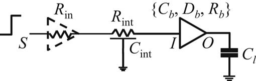
Let Rin denote the output resistance of a buffer driving a second buffer. The load capacitance of the buffer is denoted by Cl. Interconnects with diverse impedance characteristics are modeled by employing different Rint and Cint, where Rint and Cint denote, respectively, the resistance and capacitance of the interconnects. The interconnect Rint and Cint can also be adjusted to produce different slew rates for the input signal of the buffer shown in Fig. 17.6.
For a step input signal, the Elmore delay [414] from source S to nodes I and O (in Fig. 17.6) is, respectively,
(17.13)
(17.14)
(17.15)
(17.16)
where Cb, Rb, and Db are, respectively, the input capacitance, output resistance, and intrinsic delay of the buffer. Variations of Cb, Rb, and Db are, respectively, denoted by ΔCb, ΔRb, and ΔDb. For the buffer shown in Fig. 17.6, Rin is considered constant (for the moment).
Through several Monte Carlo simulations, the delay variation at nodes I and O is measured by setting Cl to zero (corresponding to ![]() ) and a different value (e.g., 200 fF, corresponding to
) and a different value (e.g., 200 fF, corresponding to ![]() ). The mean value and standard deviation of ΔCb, ΔRb, and ΔDb are obtained from (17.14) and (17.16) [636]. Assuming that process variations can be described by a Gaussian distribution, the electrical characteristics of a buffer can also be approximated by a Gaussian distribution [637],
). The mean value and standard deviation of ΔCb, ΔRb, and ΔDb are obtained from (17.14) and (17.16) [636]. Assuming that process variations can be described by a Gaussian distribution, the electrical characteristics of a buffer can also be approximated by a Gaussian distribution [637],
(17.17)
![]() is characterized from (17.14). According to (17.14) and (17.16),
is characterized from (17.14). According to (17.14) and (17.16), ![]() is dependent on
is dependent on ![]() ,
, ![]() , and
, and ![]() , and the covariance
, and the covariance ![]() among these variables is
among these variables is
(17.18)
(17.19)
(17.20)
![]() is obtained from (17.18) by substituting
is obtained from (17.18) by substituting ![]() and
and ![]() , respectively, into (17.19) and (17.20).
, respectively, into (17.19) and (17.20).
Consider that ΔCb, ΔRb, and ΔDb are used to obtain the delay variation of each buffer stage Δdi, which is similar to ΔDSO. When calculating ![]() (similar to recalculating
(similar to recalculating ![]() through (17.18)),
through (17.18)), ![]() ,
, ![]() , and
, and ![]() are again substituted into (17.18). In this procedure, the covariances, cov(Db, Rb), cov(Db, Cb) and cov(Cb, Rb), effectively cancel. Consequently, the correlation among ΔCb, ΔRb, and ΔDb does not significantly affect Δdi as long as Δdi is based on this same correlation. Since ΔCb, ΔRb, and ΔDb originate from the same source of process variations, these variables are assumed in this model to be fully correlated.
are again substituted into (17.18). In this procedure, the covariances, cov(Db, Rb), cov(Db, Cb) and cov(Cb, Rb), effectively cancel. Consequently, the correlation among ΔCb, ΔRb, and ΔDb does not significantly affect Δdi as long as Δdi is based on this same correlation. Since ΔCb, ΔRb, and ΔDb originate from the same source of process variations, these variables are assumed in this model to be fully correlated.
17.2.2 Delay Distribution of Clock Paths
The buffer delay model described in the previous subsection is used to evaluate the delay distribution of clock paths in 3-D circuits. An example of a 3-D clock path is illustrated in Fig. 17.7. The devices in different physical tiers are connected by TSVs [181], which, in turn, are modeled as RC wires of different resistance and capacitance as compared to the horizontal wires (e.g., RTSV and CTSV in Fig. 17.7). RTSV and CTSV are considered fixed.
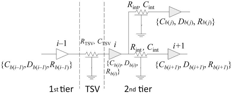
Consider the clock path consisting of buffers i−1, i, and i+1. From (17.14) and (17.16), the delay variation Δdi attributed to the variation of buffer i along a target path is
(17.21)
(17.22)
(17.23)
where the prime (′) denotes the nominal value. For buffer i, the ΔRb(i−1) of the upstream buffer and ΔCb(i+1) of the downstream buffer are both included in (17.21). To determine the delay of a clock path, Δdi for all of the buffers along this path is summed. In this case, ΔRb(i−1)ΔCb(i) and ΔRb(i)ΔCb(i+1) are duplicated. One of these two terms therefore needs to be removed. Consequently, Δdi is rewritten as
(17.24)
where
(17.25)
The variation of ΔCb is relatively low as compared with the nominal Cb (σ/μ<3% for both D2D and WID variations, as reported in Table 17.1). The observed delay variation of the buffers is also typically much lower than the nominal value (e.g., σ/μ≤5% for both D2D and WID variations, as reported in [638]). δi can be approximated using a first order linear Taylor series expansion around zero [637],
(17.26)
Table 17.1
Variations in the Electrical Characteristics of the Buffers
| Input Slew | Rb (Ω) | Cb (fF) | Db (ps) | ||||||
| μ | σWID | σD2D | μ | σWID | σD2D | μ | σWID | σD2D | |
| 47 (mV/ps) | 371 | 18.8 | 15.3 | 4.9 | 0.04 | 0.03 | 19.9 | 1.04 | 0.85 |
| σ/μ | 5.1% | 4.1% | σ/μ | 0.8% | 0.7% | σ/μ | 5.2% | 4.3% | |
| 16 (mV/ps) | 349 | 17.8 | 14.7 | 5.7 | 0.31 | 0.16 | 24.8 | 1.49 | 1.21 |
| σ/μ | 5.1% | 4.2% | σ/μ | 2.3% | 2.1% | σ/μ | 6.0% | 4.9% | |
| 6 (mV/ps) | 345 | 16.7 | 13.7 | 7.2 | 0.08 | 0.06 | 30.1 | 2.19 | 1.79 |
| σ/μ | 4.8% | 4.0% | σ/μ | 1.1% | 0.9% | σ/μ | 7.3% | 5.9% | |

As reported in Table 17.1 and discussed in [632,638] and [639], σ/μ of the transistor characteristics is typically less than 5%. The 3σ variation is smaller than 15% of the nominal Rb and 10% for ΔCb. Since ΔCb and ΔRb are modeled as Gaussian distributions, for more than 99.7% of buffers, ΔCbΔRb is lower than 1.5% CbRb. Moreover, from the nominal value and standard deviation of Cb, Rb, and Db, as reported in Table 17.1, 0.69ΔCbΔRb and 0.69CbRb are, respectively, much lower than ΔDb and Db. Consequently, approximating δi with (17.26) does not introduce a significant loss of accuracy.
As mentioned previously, ΔRb(i), ΔCb(i), and ΔDb(i) are approximated as Gaussian distributions and can be assumed to be fully correlated. According to (17.24) and (17.26), Δdi is approximated as a Gaussian distribution.
(17.27)
(17.28a)
(17.28b)
(17.29)
The terms σ1 to σ8 are, respectively,
The correlation between buffers i and j is denoted by corr(i, j). A model describing this spatial correlation is discussed in Appendix E.
Consequently, for a 3-D clock path to a sink u that includes nu clock buffers, the variation of the delay is expressed as the summation of (17.24) of each buffer along the path. The variance of the distribution of a 3-D clock path is a Gaussian distribution consisting of WID and D2D variations of the buffers,
(17.30)
(17.31)
The variation of the delay of a 3-D clock path due to D2D process variations is the sum of the D2D variations of the buffer delay in all of the tiers,
(17.32)
(17.33)
where m is the number of tiers spanned by the clock tree. ![]() is the variation of the delay of the clock path from the clock source to sink u in tier j. The number of buffers located in tier j along this clock path is denoted by nu(j). The variation of the delay related to the ith buffer in tier j is denoted by
is the variation of the delay of the clock path from the clock source to sink u in tier j. The number of buffers located in tier j along this clock path is denoted by nu(j). The variation of the delay related to the ith buffer in tier j is denoted by ![]() . Since the D2D variations equally affect the buffers within the same tier, according to (17.27), (17.28), and (17.32), the distribution of
. Since the D2D variations equally affect the buffers within the same tier, according to (17.27), (17.28), and (17.32), the distribution of ![]() is a Gaussian distribution. The D2D variations affect the buffers in different tiers independently and, therefore,
is a Gaussian distribution. The D2D variations affect the buffers in different tiers independently and, therefore, ![]() is independent of
is independent of ![]() for any j ≠ k. Consequently, according to (17.32), the distribution of
for any j ≠ k. Consequently, according to (17.32), the distribution of ![]() is also a Gaussian distribution,
is also a Gaussian distribution,
(17.34)
(17.35)
Alternatively, the variation of the delay of a 3-D clock path affected by WID variations is the sum of the WID variations of all of the buffers along this path. Consequently, according to (17.29), the distribution of ![]() is also a Gaussian distribution. The resulting variance of the delay of sink u due to WID variations is
is also a Gaussian distribution. The resulting variance of the delay of sink u due to WID variations is
(17.36)
(17.37)
where corr(i, j) is the correlation between the WID variations of buffers i and j. If buffers i and j are located in different tiers, corr(i, j)=0. The correlation of the impact of WID variations on different buffers within the same tier can be classified as systematic or random. The systematic WID variations typically exhibit a spatial correlation [638,640–642]. For those buffers located within the same tier, two types of correlations for WID variations exist, as described in Appendix E.
17.2.3 Clock Skew Distribution in Three-Dimensional Clock Trees
The clock skew between any pair of sinks in a 3-D clock tree is the difference in the clock delay between these sinks. For a 3-D clock tree with nsink sinks distributed in m tiers, the nominal and variation of the clock skew su,v between sinks u and v are, respectively,
(17.38)
(17.39)
The mean value of Δsu,v is E(Δsu,v)=E(![]() )=E(
)=E(![]() )=0. The terms ΔDuWID−ΔDvWID and ΔDuD2D−ΔDvD2D are independent. Consequently,
)=0. The terms ΔDuWID−ΔDvWID and ΔDuD2D−ΔDvD2D are independent. Consequently, ![]() and
and ![]() are treated separately. The correlation between every two terms in the expression of
are treated separately. The correlation between every two terms in the expression of ![]() is one or zero (i.e., respectively, fully correlated or uncorrelated). According to (17.32),
is one or zero (i.e., respectively, fully correlated or uncorrelated). According to (17.32), ![]() is the sum of the terms in different tiers,
is the sum of the terms in different tiers,
(17.40)
where ![]() is the D2D delay variation related to the ith buffer in the jth tier along the clock path ending at sink u. The number of buffers in the jth tier along this path is denoted as nu(j).
is the D2D delay variation related to the ith buffer in the jth tier along the clock path ending at sink u. The number of buffers in the jth tier along this path is denoted as nu(j).
All of the buffers in the same tier are equally affected by D2D variations, meaning that the correlation between each pair of variables in (17.40) is one. Since ![]() and
and ![]() are both modeled as a Gaussian distribution,
are both modeled as a Gaussian distribution, ![]() is also a Gaussian distribution. In (17.40), ∀ j1 ≠ j2 (1≤j1, j2≤m)
is also a Gaussian distribution. In (17.40), ∀ j1 ≠ j2 (1≤j1, j2≤m) ![]() is independent of
is independent of ![]() . Consequently,
. Consequently, ![]() is also described by a Gaussian distribution,
is also described by a Gaussian distribution,
(17.41)
(17.42)
According to (17.37), the distribution of ![]() is also a Gaussian distribution,
is also a Gaussian distribution,
(17.43)

(17.44)
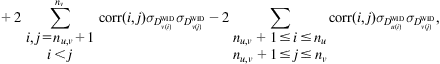 (17.44)
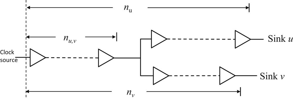
where nu,v is the number of buffers shared by the clock paths ending at sinks u and v, as depicted in Fig. 17.8. Downstream the buffers nu,v, the subpaths to u and v do not share a buffer.
According to (17.39) through (17.44), the variation of the clock skew Δsu,v between sinks u and v in a 3-D clock tree is modeled as a Gaussian distribution,
(17.45)
If the maximum tolerant skew variation is ΔS≥0, the probability that a 3-D clock tree satisfies this constraint is
(17.46)
(17.47)