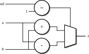
Chapter 3
Combinational Logic
This chapter will describe the basics of VHDL required to describe combinational logic using basic types to create boolean equations and simple arithmetic circuits.
It will also introduce the simulation model of VHDL, with an introduction to modelling concurrency, how this is done using the event model and the concepts of simulation time and delta time.
This chapter will then show how this model is used by synthesis tools to control the mapping of VHDL descriptions to circuits, and introduces synthesis templates.
Design Units are the basic building blocks of VHDL. They are indivisible in that a design unit must be completely contained in a single file. A file may contain any number of design units.
When a file is analysed using a VHDL simulator or synthesiser, the file is, in effect, broken up into its individual design units and each design unit is analysed separately as if they had been in separate files.
There are six kinds of design units in VHDL. These are:
- entity;
- architecture;
- package;
- package body;
- configuration declaration;
- context declaration.
The six kinds of design unit are further classified as primary or secondary units. A primary design unit can exist on its own. A secondary design unit cannot exist without its corresponding primary unit. In other words, it is not possible to analyse a secondary unit before its primary unit is analysed. The secondary units are shown above indented and immediately below their corresponding primary units.
The entity is a primary design unit that defines the interface to a circuit. Its corresponding secondary unit is the architecture that defines the contents of the circuit. There can be many architectures associated with a particular entity, but this feature is rarely, if ever, used in synthesis and so will not be covered here.
The package is also a primary design unit. A package declares types, subprograms, operations, components and other objects that can then be used in the description of a circuit. The package body is the corresponding secondary design unit that contains the implementations of subprograms and operations declared in its package. This will not be covered yet, but the usage of packages supplied with the synthesiser is covered throughout the book and how to declare your own is covered in Chapters 10 and 11.
The configuration declaration is a primary design unit with no corresponding secondary. It is used to define the way in which a hierarchical design is to be built from a range of subcomponents. However, it is not generally used for logic synthesis and will not be covered in this book.
The context declaration is a new primary unit with no corresponding secondary, and was added in VHDL-2008. It allows multiple context clauses (i.e. library and use clauses) to be grouped together. However, because it is not in common use it will not be used in this book, except in Chapter 6 where other VHDL-2008 features are discussed.
3.2 Entities and Architectures
An entity defines the interface to a circuit and the name of the circuit. An architecture defines the contents of the circuit itself. Entities and architectures therefore exist in pairs – a complete circuit description will generally have both an entity and an architecture. It is possible to have an entity without an architecture, but such examples are generally trivial and of no real use. Also, it is possible to have multiple architectures for a single entity, each one representing a different implementation of the same circuit. This can be useful when comparing different levels of model, such as comparing the RTL model with the gate-level model. It is not possible to have an architecture without an entity.
An example of an entity is:
entity adder_tree is
port (a, b, c, d : in integer; sum : out integer);
end entity adder_tree;
In this case, the circuit adder_tree has five ports: four input ports and one output port. Note that the repeat of the keyword entity and the circuit name adder_tree after the end are both optional and in practice are usually omitted.
The structure of an architecture is illustrated by the following example:
architecture behaviour of adder_tree is
signal sum1, sum2 : integer;
begin
sum1 <= a + b;
sum2 <= c + d;
sum <= sum1 + sum2;
end architecture behaviour;
The architecture has the name behaviour and belongs to the entity adder_tree. It is common practice to use the architecture name behaviour for all synthesisable architectures. As with the entity, the repeat of the architecture keyword and name behaviour after the end is optional and usually omitted. Common alternatives to architecture behaviour are architecture RTL or architecture synthesis. Architecture names do not need to be unique, indeed the consistent use of the same architecture name throughout a VHDL design is considered best-practice because it makes it easy to tell at a glance whether a VHDL description is system level (architecture system), RTL (architecture behaviour) or gate-level (architecture netlist). It does not matter what naming convention is used for architectures but it is recommended that a consistent naming convention is adhered to.
The architecture has two parts.
The declarative part is the part before the keyword begin. In this example, additional internal signals have been declared here. Signals are similar to ports but are internal to the circuit.
A signal declaration looks like:
signal sum1, sum2 : integer;
This declares two signals called sum1 and sum2 that have a type called integer. Basic types will be dealt with in Chapter 4, and a set of synthesis-specific types are covered in Chapter 6, so for now it is sufficient to say that integer is a numeric type that can be used for calculations.
The statement part is the part after the begin. This is the description of the circuit itself. In this example the statement part only contains signal assignments describing the adder tree as three adders described by equations.
The simple signal assignment looks like:
sum1 <= a + b;
The left-hand side of the assignment is known as the target of the assignment (in this case sum1). The assignment itself has the symbol "< = " that is usually read ‘gets’, as in ‘signal sum1 gets a plus b’.
The right-hand side of the assignment is known as the source of the assignment. The source expression can be as complex as you like. For example, the circuit of the adder_tree example could have been written using just one signal assignment:
sum <= (a + b) + (c + d);
The example was written with three assignments so that the relationship between assignments, ports and signal declarations could be explained.
In this example, the statements have been written in sequence so that the data flow is from top to bottom. However, this is done for readability only; the ordering of the statements is irrelevant. This is because each statement simply defines a relationship between its inputs (the source, on the right-hand side of the assignment) and its output (the target, on the left-hand side).
For example, the following architecture is functionally equivalent to the previous version:
architecture behaviour of adder_tree is
signal sum1, sum2 : integer;
begin
sum <= sum1 + sum2;
sum2 <= c + d;
sum1 <= a + b;
end;
In order to really understand how VHDL works, it is useful to have a basic knowledge of the underlying mechanisms of the language. This will help to explain many VHDL features introduced in this and subsequent chapters.
VHDL has been designed from the start as a simulation language, so an understanding of the language must come from examining the behaviour of a VHDL simulator. The definition of VHDL contained in the Language Reference Manual includes a definition of how a simulator should implement the language, so this behaviour must be common to all VHDL simulators.
The basis of VHDL simulation is event processing. All VHDL simulators are event-driven simulators.
There are three essential concepts to event-driven simulation. These are: simulation time, delta time and event processing.
During a simulation, the simulator keeps track of the current time that has been simulated, that is, the circuit time that has been modelled by the simulator, not the time the simulation has actually taken. This time is known as the simulation time and is usually measured as an integral multiple of a basic unit of time known as the resolution limit. The simulator cannot measure time delays less than the resolution limit. For gate-level simulations the resolution limit may be quite fine, possibly 1 fs or less. For RTL simulations, there is no need to specify a fine resolution since we are only interested in clock-cycle by clock-cycle behaviour and the transfer functions are described with zero or unit time delay. In this case, a resolution limit of 1 ps is often used. It is important to note that the resolution limit is a characteristic of the simulator, not of the VHDL model. It is usually controlled by a simulator configuration setting.
The simulation cycle alternates between event processing and process execution. Put another way, signals are updated as a batch in the event processing part of the cycle, then processes are run as a batch in the process execution part. The signal updating and process execution are kept completely separate. This is how VHDL models concurrency such that it can be modelled on a sequential computer processor without having to use multiple processors or threads.
When a signal assignment (a simplified process) is performed, the signal that is the target of the assignment is not updated immediately by the assignment; in fact it keeps its old value for the remainder of the process execution phase. Instead, the assignment causes a transaction to be added to a queue of transactions associated with the driver of the signal.
For example:
a <= '0' after 1 ns, '1' after 2 ns;
This signal assignment queues two transactions in the driver for signal a. The first transaction has the value '0' and a time delay of 1 ns; the second transaction has the value '1' and a time delay of 2 ns. It is also possible to have a zero-delay assignment:
a <= '0';
This contains one transaction with the value of '0' and no time delay. Even when there is no time delay the signal is not updated immediately, since the transaction will be scheduled for the next delta cycle.
When simulation time moves on to the point where a transaction becomes due on a signal, then during the event-processing phase that signal becomes active. The new value is then compared with the old value and, if the value has changed, then an event is generated for that signal. This event causes processes sensitive to the signal to be triggered. Note that, if the signal is assigned a value that is the same as its current value, it will become active but will not have an event and so will not trigger any processes.
An event is processed by updating the signal value, then working out which statements have that signal as an input (in VHDL-speak, all the statements that are sensitive to that signal). All signals are processed as a batch, that is, all signals that have an event in the current simulation cycle are updated in this way. The set of processes triggered by these signal updates are scheduled for execution during a later process execution phase. Each process can only be triggered once per simulation cycle, no matter how many of its inputs change.
During the process execution phase, each process is executed until it pauses. The simulator works its way through all the triggered processes in no particular order executing them until they pause. Only after all the triggered processes have paused will the simulator switch back to the event-processing phase.
Any signal assignments in the executed processes cause more transactions to be generated. These new transactions are processed in later simulation cycles. Zero-delay assignments will be processed in the next delta cycle.
The distinction between an active signal and a signal event is very important. Processes are sensitive to events, so will only be activated by a signal changing its value. This is generally what is wanted. For example, consider the following RS latch model:
P1: process (R, Qbar)
begin
Q <= R nor Qbar;
end process;
P2: process (S, Q)
begin
Qbar <= S nor Q;
end process;
This example has been written using processes to show the sensitivity list. This is the list of signals in parentheses after the keyword process, which represents the set of signals that will trigger the process. For combinational logic, the sensitivity list should include all of the inputs of the process, in this case all of the signals on the source (right-hand) side of the signal assignments.
The example could have been written without processes, using just simple signal assignments:
P1: Q <= R nor Qbar;
P2: Qbar <= S nor Q;
This is exactly equivalent since the VHDL standard states that a signal assignment has an implied sensitivity list containing all the signals on its right-hand side. In other words, assignment P1 will trigger on changes to R or Qbar, whilst assignment P2 will trigger on changes to S or Q.
Consider the case when R and S are '0', with Q at '1' and Qbar at '0'. Consider what then happens when R changes due to a transaction of value '1' at the current simulation time. The model will go through the following sequence:
delta 1, event processing
The transaction makes R active and, since it is a change in value for R (from '0' to '1'), it causes an event on R. The event on R triggers process P1 that is sensitive to it.
delta 1, process execution
P1 recalculates the value of Q, creating a transaction of value '0' (since '1' nor '0' is '0') at the current time. This transaction is added to the transaction queue for Q.
delta 2, event processing
The transaction on Q makes Q active and, since it is a change in value for Q (from '1' to '0'), it causes an event on Q. The event on Q triggers process P2 that is sensitive to it.
delta 2, process execution
P2 recalculates the value of Qbar, creating a transaction of value '1' (since '0' nor '0' is '1') at the current time. This transaction is added to the transaction queue for Qbar.
delta 3, event processing
The transaction on Qbar makes Qbar active and, since it is a change in value for Qbar (from '0' to '1'), it causes an event on Qbar. The event on Qbar triggers process P1 for the second time.
delta 3, process execution
P1 recalculates the value of Q, creating a transaction of value '0' (since '1' nor '1' is '0') at the current time. This transaction is added to the transaction queue for Q.
delta 4, event processing
The transaction on Q makes Q active but, since it is not a change in value for Q (from '0' to '0'), it does not cause an event on Q.
Since there are no more transactions to process in the model, the model reaches a stable state at this point. The simulation time can now be moved on to the next scheduled transaction on R or S and a similar series of delta cycles will be carried out.
The important thing about the way VHDL models the circuit is that the signal/process delta cycles stopped because a transaction did not result in a change in a signal, so no events were generated, even though a signal did become active in the last cycle. As you can see from this example, this means that VHDL models asynchronous feedback simply and naturally. It also means that the order in which the processes or signal assignments are listed in the architecture has no effect on the simulation, since the decisions determining which processes to execute are based purely on the events and process sensitivity lists, not on the order of the statements. Swapping the two processes would result in exactly the same sequence. VHDL is a concurrent language.
Note: you would never model a latch like this in RTL, it was just used to illustrate how VHDL models feedback correctly.
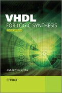
To further illustrate the action of an event-driven simulator to show how values propagate through a circuit, consider the behaviour of the adder_tree example introduced earlier.
For this example, it will be assumed that the circuit is initially in a stable state with all the inputs set to 0. It can be seen from the description of the adder tree that all the internal signals and the outputs will also be 0. These values are set up during the initialisation (or elaboration) phase of simulation, which happens at time zero.
Consider what happens if the input b changes from 0 to 1 at a simulation time of 20 ns. This means that a transaction is generated for signal b and this transaction is posted at the first delta cycle of the 20 ns simulation time. When this transaction is processed, it is tested to see if it is a change in value, which it is, so this causes an event on b. The event processing causes the equations that are sensitive to b to be triggered. These are:
sum1 <= a + b;
So this equation is executed during the process execution phase. As a result of recalculating this equation, a transaction is generated for sum1 at the current simulation time (20 ns), but at the next delta cycle. At this stage, signal sum1 has not changed value; the only outcome of the process execution is that a transaction is posted for sum1 specifying a new value of 1 (i.e. 0 + 1) for signal sum1.
The next stage of the simulation is transaction processing of the second delta cycle. First, the transaction on signal sum1 is tested to see if it changes its value, which it does, so the transaction is transformed into an event.
Then, all equations sensitive to sum1 are triggered. The sensitive equations are:
sum <= sum1 + sum2;
Process execution is carried out on this equation, generating transactions for the next delta cycle. One new transaction is generated in this case and posted at the third delta cycle at the current simulation time. The transaction is a new value for sum2 of 1. Once again, this value is not yet assigned to the signal.
Transaction processing of the third delta cycle causes the transaction on sum to be tested to see if it represents a change of value. Once again it is a change, so the transaction is transformed into an event, triggering equations sensitive to it. No equations are sensitive to the output signals, so there are no further transactions to process and simulation of the current simulation time has now completed. Simulation time can now be moved on.
The whole simulation cycle is summarised in Table 3.1.
Table 3.1 Event processing of adder tree.
Note how the change on the input propagated through to the sum output over three delta cycles. The result is that a minimum set of processes was re-executed as a result of the input change and that some processes were not re-executed at all.
Since VHDL has been designed as a simulation language without regard to the needs of synthesis or any other application area, synthesisers must make an interpretation of the language. This interpretation is based on mappings of special VHDL constructs onto hardware with equivalent behaviour.
These special constructs are known as templates.
The mapping is not always straightforward. Some VHDL constructs have direct one-to-one mappings to hardware equivalents. Many VHDL constructs have no possible hardware equivalents, at least within the confines of logic synthesis, and these will cause errors during synthesis. Other constructs have to meet specific constraints in order to be mappable. Synthesisers must impose these constraints on the use of the language so that only VHDL constructs that have hardware equivalents can be used. In other words, your VHDL must conform to the appropriate template for the hardware structure you wish to build.
There are templates for combinational logic, simple registers, registers with asynchronous reset, registers with synchronous reset, latches, RAMs, ROMs, tristate drivers and finite-state machines, all of which will be covered later in this book.
Note: you might come across the synthesis subset of VHDL expressed as a restricted syntax. This is unhelpful since the synthesis subset is really a semantic subset. That is, most VHDL constructs are synthesisable provided that they are used in a particular, constrained way that fits one of the synthesis templates.
It is extremely important to conform to these templates since they dictate how VHDL must be written in order to be synthesisable. VHDL models must be written for synthesis from the start; it is not possible to take just any VHDL that simulates correctly and expect it to be synthesisable. Many person-years of work have been wasted by engineers who failed to realise this and wasted their time perfecting simulation models before considering the synthesis constraints.
Fortunately, in the case of the adder_tree example, the circuit interpretation is a simple and direct mapping to hardware. VHDL signal assignments map directly onto blocks of combinational logic. This can be seen by considering the event processing cycle described earlier. At each stage, every equation that is sensitive to a changing input is recalculated. This is the behaviour of combinational logic in which the output is re-evaluated whenever an input changes. The expressions used (+ operators) have direct equivalents in hardware too. These equivalences together give us the mapping from simulation behaviour to circuit structure.
In later chapters, similar parallels will be drawn to show how the simulation model of other constructs can be mimicked by certain hardware structures. It is this mimicry that gives us the hardware mapping. It should always be remembered that VHDL is a simulation language and that not all simulation constructs have hardware equivalents. This is why all synthesisers must work on subsets of the language.
Figure 3.1 illustrates the circuit representation of the adder_tree entity/architecture pair.
Figure 3.1 Adder tree circuit.

In this figure, the operations have been represented by simple circles rather than as gates to highlight the fact that, at this stage, there has been no mapping to gates. Instead the circuit has been shown as a network of abstract arithmetic functions. A synthesiser will usually restructure these arithmetic functions to match actual gates in the target technology library at a late stage in the synthesis process known as the technology mapping stage. In this case the functions would be restructured into a full-adder circuit, but the exact type of adder will depend on the target technology and the speed and area constraints being use for the synthesis. For clarity in this discussion, the synthesis process has been frozen prior to this technology mapping phase so that the intermediate structure can be seen. All synthesisers perform synthesis in stages, starting with the interpretation of the source VHDL to form a functional network, followed by optimisation of the functional network and then finally technology mapping.
Signals are the carriers of data values around an architecture. Ports are the same as signals but also provide an interface through the entity so that the entity can be used as a subcircuit in a hierarchical design.
A signal is declared in the declarative part of an architecture (between the keywords is and begin) and the declaration has two parts:
architecture behaviour of adder_tree is
signal sum1, sum2 : integer;
begin
...
The first part of the declaration is the keyword signal and a list of signal names: in this case there are two signals sum1 and sum2. The second part, after the colon, is the type of the signals: in this case integer.
There can be many signal declarations in an architecture, each terminated by a semi-colon. The above declaration could be rewritten as two separate declarations:
architecture behaviour of adder_tree is
signal sum1 : integer;
signal sum2 : integer;
begin
...
Port declarations are enclosed by a port specification in the entity. The port specification has the following structure:
entity adder_tree is
port (port specification );
end;
Note that the port specification is enclosed in parentheses and always terminated by a semi-colon that is outside the parentheses.
A port is declared within the port specification. A port declaration has three parts:
entity adder_tree is
port (a, b, c, d : in integer; sum : out integer);
end;
Looking at the first declaration in the port list, the first part is a list of port names: in this case a, b, c and d. The second part is the mode of the port: in this case the mode is in. The third part is the type as in the signal declaration: in this case the type is integer.
Each port declaration within the specification is separated by semi-colons from the others. Note that, unlike the signal declarations, which are each terminated by a semi-colon, port declarations are separated (not terminated) by semi-colons, so there is no semi-colon after the last declaration before the closing parenthesis.
The mode of a port determines the direction of data flow through the port. There are five port modes in VHDL: in, out, inout, buffer and linkage. If a mode is not given, then mode in will be assumed.
The meanings of the modes as they are used for logic synthesis are:
| in | input port – cannot be assigned to in the circuit, can be read |
| out | output port – can be assigned to in the circuit, cannot be read |
| inout | bidirectional port – can only be used for tristate buses |
| buffer | output port – like mode out but can also be read |
| linkage | not used by synthesis |
There is often confusion between mode out and mode buffer. Mode buffer is an anachronism and the reason for its existence in the language is obscure. The full behaviour of a buffer port is a restricted form of mode inout. However, to make the mode usable for synthesis, the rules for buffer ports are constrained so that they act like mode out ports with the added convenience that it is possible to read from the port within the architecture. There really is no reason to have two output modes, so it is recommended that only out mode is used.
So the port modes as recommended for use in logic synthesis are:
| in | input port |
| out | output port |
| inout | bidirectional port for tristate buses |
There is a problem if you need to read from an out mode port. This problem is illustrated by the following example of an and gate with true and inverted outputs. The first version shows an illegal description, because the out port z is read:
entity and_nand is
port (a, b : in bit;
z, zbar : out bit);
end;
architecture illegal of and_nand is
begin
z <= a and b;
zbar <= not z;
end;
The solution is to use an intermediate internal signal and read from that. The intermediate signal can then be assigned to the out mode ports.
The corrected example is:
entity and_nand is
port (a, b : in bit;
z, zbar : out bit);
end;
architecture behaviour of and_nand is
signal result : bit;
begin
result <= a and b;
z <= result;
zbar <= not result;
end;
It is good practice to always use intermediate signals for outputs and to assign them to the out ports at the end of the architecture. By doing this consistently, the pitfall of trying to read an out port is always avoided.
Note: in VHDL 2008, it is possible to read from out ports, thus making it unnecessary to have the intermediate signal. Therefore, in a few years time when VHDL-2008 becomes the norm, this problem will go away.
All signals have an initial value when simulation begins. This initial value can either be user-supplied in the signal (or port) declaration or will be given by default. The simulator will assign these initial values to signals during the elaboration phase of simulation.
Initial values given in the signal declaration look like this:
signal a : bit := '1';
This means that, at the start of simulation, signal a will take the value '1'.
If a signal does not have an explicit initial value given in the signal declaration, the signal will still have an initial value in simulation. This value will be the first value (referred to as the left value because it will appear on the left if you list the values in order) of the type. For type bit (see Chapter 4), the left value is '0', so all signals of type bit will be initialised with the value '0' unless an explicit initial value is used to override it. Signals of type std_logic (see Chapter 5) will initialise to the value 'U' that signifies an undefined value.
The rules for initial values ensure that all simulations start from the same, known, state. This means that identical simulations will give identical results even on different simulators.
For synthesis, there is no hardware interpretation of an initial value. It is not possible to initialise all signals in a circuit with a known value on power-up. Even though it is possible to do a power-on reset in some logic technologies, it would not be desirable to do this for every wire in the circuit. So, synthesis must ignore initial values.
This opens up a potential pitfall that is a common cause of circuit failure for a synthesis-generated design. That is, the synthesised circuit will not start up in a known state and will not therefore behave in the same way as the simulation predicted. It may even get permanently stuck in an unknown state that doesn't exist in the simulation model.
The point is that this is not a failure of the synthesiser, since the synthesiser must ignore initial values – it is the designer's responsibility to provide a mechanism for putting the circuit into a known state, either in the form of a global reset input to the system or by designing circuits so that they can be put into a known state in some other way such as by making the controller state machine re-entrant. The design of a reset or initialisation mechanism is an essential part of the RTL design process and must not be skipped. Generally it is registers that need to be reset or initialised, so the details of how to implement register resets will be deferred to Chapter 9.
One way of testing a reset mechanism is to give the internal signals undefined initial values (i.e. use std_logic for all signals) and then ensure that the simulation gives expected, defined results. This doesn't guarantee that the design is correct, but it is impractical to try all possible initial values, so the only real way of ensuring correct initialisation behaviour is by structured and rigorous design.
The simple signal assignment statement has already been used in the adder_tree example. This section examines the signal assignment statement in more detail.
The simple signal assignment looks like this:
sum1 <= a + b;
The left-hand side of the assignment is known as the target of the assignment (in this case sum1). The right-hand side of the assignment is known as the source expression of the assignment (in this case a + b). The assignment itself is the symbol <= that is formed by combining the less-than and the equals symbols to form an arrow. There must be no space between the two characters in the symbol. Beware of confusion with the less-than-or-equal operator <= that looks exactly the same. Fortunately, there is no real chance of confusion because there are no situations where both meanings would be allowed by the language. Nevertheless, it takes some getting used to.
The rules of VHDL insist that the source of an assignment is the same type as the target. This example uses type integer. The addition of two signals of type integer gives a result that is also an integer. Therefore, the source and target are of the same type.
The source expression can be as complex as you like. For example, the circuit of the adder_tree example could have been written using just one signal assignments:
sum <= (a + b) + (c + d);
3.8 Conditional Signal Assignments
Conditional signal assignments are signal assignments with more than one source expression, where one of the source expressions is chosen by a control condition. The simplest form of the conditional signal assignment has only one condition:
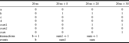
sum <= a + b when sel = '1' else a - b;
In this case, the condition is the test for sel = '1'. The test can be any boolean expression, which generally means a test for equality or inequality, or a comparison such as less-than when using integer types.
The rule for the source expressions is that they must all be the same type as the target of the assignment. In this example, the sources and the target are of type integer.
The hardware mapping of the conditional signal assignment is a multiplexer that selects between the source expressions and that is controlled by the condition expression. Figure 3.2 shows the circuit of this example.
Figure 3.2 Hardware mapping of conditional signal assignment.
In the figure, the condition has been shown explicitly as a test for the equality of sel and the value '1'. This is the circuit that a synthesiser will map the VHDL onto initially, but the equality operator will be easily minimised to a single piece of wire such that sel controls the multiplexer directly. This kind of minimisation is routine in synthesis and it means that you don't have to worry about the exact implementation of the circuit.
This example is the simplest form of conditional signal assignment, with only one condition. It is possible to have any number of branches; each branch but the last has a different condition. The last branch must be an unconditional else so that one of the source expressions will always be assigned to the target. An example of a multiple-branch conditional signal assignment is:
z <= a when sel1 = '1' else
b when sel2 = '1' else
c;
The conditions are evaluated in the order that they are written and the first condition that is true will be selected. This is equivalent in hardware terms to a series of two-way multiplexers, with the first condition controlling the multiplexer nearest to the output so that that condition overrides any of the later conditions.
The circuit for this example is illustrated in Figure 3.3.
Figure 3.3 Multi-way conditional signal assignment.

In this example, the conditions have already been optimised so that sel1 and sel2 control the multiplexers directly. It can be seen from this circuit that when sel1 is '1', then a is selected regardless of the value of sel2. If sel1 is '0', then sel2 selects between b and c inputs.
With more branches, extra multiplexers are added to the structure so the result is a long chain of multiplexers. The chain will be skewed, not symmetrical, because of the precedence rules just described. This should be taken into account in the design; the further down the list of selections a source is, the more multiplexers it will pass through when synthesised.
A similar structure can be created by the if statement (see Section 8.4) which allows more complex structures; in particular it allows more than one signal to be assigned in each branch of the conditional.
Each condition in a conditional signal assignment is assumed to be independent of the others when mapping onto hardware. This means that, if the conditions are dependent (based on the same signal, for example), then there won't necessarily be any optimisation. For example:
z <= a when sel = '1' else
b when sel = '0' else
c;
In this example, the second condition is dependent on the first. In fact, in the second branch, sel can only possibly be '0', since the first condition would have been true if sel was '1'. Therefore, the second condition is a redundant one and the final else branch cannot be reached. In synthesis, this conditional signal assignment would still be mapped onto two multiplexers as shown in Figure 3.4.
Figure 3.4 Redundant branch in conditional signal assignment.

With a simple example such as this, the synthesiser may identify and eliminate the redundant extra multiplexer during the logic optimisation phase of the synthesis process, but with more complex examples it could not be guaranteed to do so. Detecting redundant conditions is a very difficult task in the general case. This example was made simple to illustrate the problem, but in practice, these redundancies can be subtle and beyond the capability of logic minimisation. It is important to realise that you tend to get what you ask for in the mapping from VHDL to hardware, so if you ask for two multiplexers, that is probably what you will get.
The cause of this pitfall is the incorrect use of an extra branch in the conditional signal assignment in the first place. The point of the conditional signal assignment is that the individual conditions are independent of each other and the synthesis interpretation assumes this independence. In this example, the conditions are dependent on each other because they are repeated tests of the same signal. This should have been implemented as a two-input conditional signal assignment.
3.9 Selected Signal Assignment
Selected signal assignments, like conditional signal assignments, allow one of a number of source expressions to be selected based on a condition. The difference is that a selected signal assignment uses a single condition to select one from many branches. The condition can be of any type and therefore can select between any number of branches.
A simple example is:
with sel select
z <= a when '1',
b when '0';
The main difference between the selected signal assignment and the conditional signal assignment is that there is only one condition; all the tests have equal priority and are mutually exclusive.
This simple example could just as easily have been done with a conditional assignment, because it only has two branches, but it does illustrate the form of the selected signal assignment.
The condition in this case is the signal sel. In this example it is of type bit, but could be any type. For example, it could be a bus of signals, with a branch for each possible bit pattern on the bus. Then, the assignment itself contains a number of source expressions, each of which is selected by a given value of the condition. Here is a similar example where the selection signal is a 2-bit bus:
with sel select
z <= a when "00",
b when "01",
c when "10",
d when "11";
All values of the condition's type must be covered by the selections. A similar structure can be created by the case statement (see Section 8.5) that allows more complex structures; in particular it allows more than one signal to be assigned in each branch of the conditional.
Selected signal assignments come into their own when used with enumeration types, especially multi-valued logic types and integer types. The discussion of selected signal assignments with other types will be deferred until after the types have been covered, in Section 4.12.
3.10.1 Parity Generator
The example creates a simple 8-bit parity generator using concurrent signal assignments. The parity circuit will be switchable between two different modes depending on the values of a control input, as shown in Table 3.2.
Table 3.2 Parity-generator functions.
| Mode | Function |
| 0 | odd parity |
| 1 | even parity |
In odd parity mode, the output is 0 if the input has an odd number of ones. In even parity mode, the output is 0 if the input has an even number of ones.
The block diagram for the circuit is shown in Figure 3.5.
Figure 3.5 Parity generator interface.
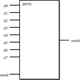
The first stage is to write the entity, based on the block diagram. This looks like:
entity parity is
port (d7, d6, d5, d4, d3, d2, d1, d0 : in bit;
mode : in bit;
result : out bit);
end;
The architecture for the solution is:
architecture behaviour of parity is
signal sum : bit;
begin
sum <= d0 xor d1 xor d2 xor d3 xor d4 xor d5 xor d6 xor d7;
result <= sum when mode = '1' else not sum;
end;
The architecture is in two parts, each a separate signal assignment. One is a simple signal assignment that calculates the parity function and assigns it to the internal signal sum. The second part is a conditional signal assignment that selects the output appropriate to the function to be performed according to the values of the control input mode.