
Chapter 12
Special Structures
This chapter is a mopping-up chapter to cover a few hardware structures that are important but that haven't fitted into the earlier chapters. These special structures have been collected together here.
The first special structure is the tristate driver, how to model this in simulation using a synthesis template and how to model tristate buses.
Then finite state machines (FSMs) are covered. These are often used to implement controllers. A variety of templates are described that provide Moore machines, Mealy machines and FSMs with either combinational or registered outputs.
The next section covers memories, which can be implemented as register banks or converted into RAMs using RAM inference. A number of different templates are described that allow different types of RAM to be inferred.
Finally, decoders are described, which can be converted into ROMs using ROM inference.
There are two aspects to the modelling of tristate systems in VHDL. One covers the modelling of tristate drivers. The other is the modelling of tristate buses.
Tristate drivers are hardware structures that have to be recognised as templates, since there is no direct mapping from VHDL to tristate drivers. In other words, a synthesiser has to perform tristate inference, just as it has to perform latch inference and register inference.
The most common tristate driver template uses sequential VHDL to model tristate behaviour. This means that tristate drivers must be modelled as processes. It is possible to write a concurrent signal assignment (using conditional assignments) that has the behaviour of a tristate driver, but most synthesisers will not recognise it as a tristate driver because it does not match the template.
Tristate buses require the use of a multi-valued logic type, which can model a high-impedance value. The logic type should also be able to handle multiple drivers driving the same bus. In VHDL terms, this means that the type must be resolved, that is, capable of being the target of more than one signal assignment. In simulation, resolution is implemented as a resolution function that is called with all the values being driven onto the signal from all the tristate drivers. The resolution function then decides what value the signal should have. Resolution only applies to signals, so tristate buses must be modelled by signals and cannot be modelled by variables.
The IEEE standard type std_logic models high-impedance values as the value ‘Z’. Furthermore, it is resolved in a way that models tristate drivers. For example, if one driver is driving the value ‘1’ and another ‘Z’, then the signal gets the value ‘1’. It is not necessary to understand any more than this about the operation of a resolved type if you are using VHDL for synthesis. It is sufficient to know that the subtype std_logic is resolved for use as a tristate bus, whereas its basetype std_ulogic is not.
The tristate driver template uses a combinational process containing an if statement. An example is shown in the following VHDL code, which shows just the tristate driver process:
process (d, en)
begin
if en = '1' then
q <= d;
else
q <= 'Z';
end if;
end process;
It can be seen that this process is a combinational logic process, apparently containing a two-way multiplexer modelled by the if statement. However, since the assignment to q in one branch of the if statement is the value ‘Z’, this will be interpreted as a tristate driver. The equivalent circuit is shown in Figure 12.1.
Figure 12.1 Tristate driver.

The tristate driver is implemented in a similar way to the register. The process is implemented as if it was a combinational process (ignoring the tristate part) and then a tristate driver is added to the outputs. Because of this similarity with the register template, it is not possible to combine the two templates. In other words, it is not possible to describe a register with a tristateable output as a single process. Instead, it should be modelled by separate processes; a registered process to model the register and a combinational process to model the tristate driver on its output.
The exact rules for writing the tristate driver will vary between synthesisers. The safest template to use is as illustrated by the example above which is the simplest standardised form. Assume that the whole process will be implemented as a tristate driver and that the if statement must be in the form shown, with two branches: one containing the high-impedance assignment and the other containing any other combinational logic. Most synthesisers offer more flexibility than this, but using that extra flexibility may be non-portable between synthesisers. In any case, the use of the template makes the intention of the circuit clearer both to the original designer and to anyone else who subsequently has to work on it, so the use of this template is recommended, even if it is not obligatory.
The tristate bus is simply a signal of a subtype, known as a resolved subtype, which can model tristates. This is always std_logic or any one of its array types, since this subtype already has a resolution function that models tristates and is the only standard type that does. However, the subtype itself is not enough to make a signal a tristate – after all the subtype std_logic is generally used for all signals in a design. The other condition is that a signal is treated as a tristate bus if it has tristate drivers driving it. If any one driver of a signal is a tristate driver, then all the drivers of that signal must be tristate drivers. Furthermore, if one element of an array signal is a tristate signal, then all elements must be tristate signals.
The only other special handling of tristate signals is when they are used as ports to an entity. Tristate ports should be modelled using mode inout, so that the synthesiser knows that they must be implemented as tristate buses. This rule should be followed even if the bus is being driven by a tristate driver but is not being read. An example of this is the above example of the basic driver, shown in context in an entity/architecture pair.
library ieee;
use ieee.std_logic_1164.all;
entity tristate is
port (d : in std_logic;
en : in std_logic;
q : inout std_logic);
end;
In this entity, port q has been identified as a tristate bus and therefore it should be driven by a tristate driver.
architecture behaviour of tristate is
begin
process (d, en)
begin
if en = '1' then
q <= d;
else
q <= 'Z';
end if;
end process;
end;
Generally, tristate drivers will be mixed with other logic in an architecture. This example showed the tristate driver as the only component in the architecture for clarity, to show the relationship between the driver process and the port modes. Despite the fact that the process only writes to the port and doesn't read it, the port is inout mode.
Note: there are a lot of examples available on the Internet that show tristate buses modelled as in or out parameters. Modern synthesisers don't need the inout port class to know that a port is a tristate bus and to synthesise it correctly. However, it is still recommended practice to use inout ports for all tristate buses because it makes the interface of the entity more self-explanatory.
Array drivers can be created simply by using any array of std_logic, such as std_logic_vector and the synthesis typessigned and unsigned from numeric_std.
Note: the fixed-point and floating-point types from the VHDL-1993 compatibility versions of fixed_pkg and float_pkg cannot be used for tristates because they use std_ulogic. This problem is fixed in the VHDL-2008 versions of the packages so these types will also be usable as tristate buses when the VHDL-2008 versions become available. In the meantime, tristate buses should be implemented using std_logic_vector and the fixed and floating-point types converted to and from this type using the bit-preserving type conversions described in Section 6.7.
For tristate arrays. the assignment of the value ‘Z’ is changed into an array assignment of a string of ‘Z’ values
library ieee;
use ieee.std_logic_1164.all
use ieee.numeric_std.all;
entity tristate_vec is
port (d : in signed(7 downto 0);
en : in std_logic;
q : inout signed(7 downto 0));
end;
architecture behaviour of tristate_vec is
begin
process (d, en)
begin
if en = '1' then
q <= d;
else
q <= "ZZZZZZZZ";
end if;
end process;
end;
An alternative that is simpler to type, especially for large buses, and the only form that works for generic-sized buses, is to use an aggregate with an others clause:
q <= (others => 'Z'),
To illustrate the use of tristates in a slightly larger example, a tristateable multiplexer will be written using the synthesisable tristate template.
To keep the example clear, the design is placed in the context of a separate entity and architecture.
The entity is:
library ieee;
use ieee.std_logic_1164.all;
entity tristate_mux is
port (a, b, sel, en : in std_logic;
z : inout std_logic);
end;
There are two possible solutions to this problem: either two tristate drivers driving the same output or a multiplexer followed by a single tristate driver. Both of these two solutions will be shown.
The block diagram of the first possible implementation circuit is shown in Figure 12.2.
Figure 12.2 Tristate multiplexer using two drivers.
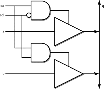
Inputs a and b are the data inputs, sel selects between a (sel = 0) and b (sel = 1). Input en enables the output driver: when en = 0 the output is high impedance.
The architecture for this two-driver solution is:
architecture behaviour of tristate_mux is
begin
t0: process (en, sel, a)
begin if en = '1' and sel = '0' then
z <= a;
else
z <= (others => 'Z'),
end if;
end process;
t1: process (en, sel, b)
begin
if en = '1' and sel = '1' then
z <= b;
else
z <= (others => 'Z'),
end if;
end process;
end;
The solution contains two copies of the template for a tristate driver. The drivers are connected straight to the tristate port z. Note that no attempt has been made to combine the two drivers into one process: this is a common mistake. The design is clearer and simpler and therefore far less error-prone if each part of the design is expressed separately in this way. There is a one-to-one correspondence with the original block diagram.
The alternative solution uses a single tristate driver with a multiplexer on its input. This solution is illustrated by Figure 12.3.
Figure 12.3 Tristate multiplexer using one driver.

Since the tristate driver process can contain other logic in the combination branch (that is, the branch without the high-impedance assignment) of the if statement, this can be expressed as a single process:
process (en, sel, a)
begin
-- tristate driver
if en = '1' then
-- multiplexer
if sel = '0' then
z <= a;
else
z <= b;
end if;
else
z <= (others => 'Z'),
end if;
end process;
Notice how the combinational part of the behaviour has been kept separate from the tristate driver part, with the multiplexer logic completely contained within the first branch of the outer if statement that represents the tristate driver.
The basic form of a finite state machine (FSM) is a sequential circuit in which the next state and the circuit outputs depend on the current state and the inputs. The most common application for FSMs is in control circuits. The basic form of an FSM is shown in Figure 12.4.
Figure 12.4 Finite state machine.
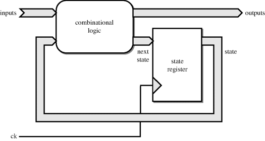
An FSM can be modelled in VHDL as a combinational block and a register block, and in that sense is nothing special. However, most synthesisers have the capability of performing state optimisation on FSMs to minimise the circuit area. This optimisation is only available if the FSM model fits one of the templates that allows FSM inference to take place.
As usual, the range of different templates vary from one synthesiser to another and some synthesisers support several other variants, but the templates presented here are the common denominator and are the recommended forms.
The key feature of the FSM templates is that the current state and next state are represented by an enumeration type, with one value for each state. The inputs and outputs can be of any type.
The example is a very simple state machine that detects a certain bit sequence (a signature) on a one-bit wide serial input. The state machine is defined by the state-transition diagram in Figure 12.5.
Figure 12.5 Signature detector state-transition diagram.
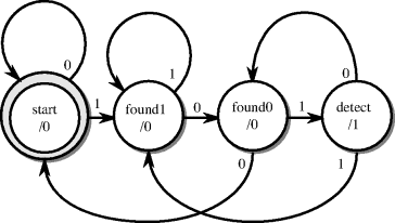
The state-transition diagram shows the states as circles with the state name inside. The states themselves are also annotated with the output value that is required from the state machine when it is in that state. The state transitions are labelled with the input value that causes the transition. This example is a Moore machine, since the output only depends on the current state and is independent of the input.
The example in VHDL is shown in context in a separate entity and architecture. In general, state machines can be mixed with other circuitry and the separation has been done purely for clarity. The entity is the same for all the examples:
library ieee;
use ieee.std_logic_1164.all;
entity signature_detector is
port (d : in std_logic;
ck : in std_logic;
found : out std_logic);
end;
12.2.1 Two Processes, Single Decoder
This variant of the FSM template puts all of the decoding logic into one combinational process with a second registered process that just generates the state register but has no logic in it.
architecture behaviour of signature_detector is
type state_type is (start, found1, found0, detect);
signal state, next_state : state_type;
begin
-- register block
process
begin
wait until rising_edge(ck);
state <= next_state;
end process;
-- combinational logic block
process (state, d)
begin
case state is
when start =>
found <= '0';
if d = '1' then
next_state <= found1;
else
next_state <= start;
end if;
when found1 =>
found <= '0';
if d = '0' then
next_state <= found0;
else
next_state <= found1;
end if;
when found0 =>
found <= '0';
if d = '1' then
next_state <= detect;
else
next_state <= start;
end if;
when detect =>
found <= '1';
if d = '1' then
next_state <= found1;
else
next_state <= found0;
end if;
end case;
end process;
end;
The combinational logic block should be modelled as a process with a case statement branching on the current value of the state. The contents of each branch of the case statement should contain simple assignments of values to the next state and output signals. Branches in the state-transition diagram are modelled by if statements within a branch of the case statement, as in this example. To model a Mealy machine, the outputs would also be conditional on the inputs, so the assignments to the outputs would also be inside the if statements.
The case statement must be complete, which means that it covers all the states, and it should be purely combinational with no latches, which means that all outputs get a value under all conditions.
This can be rewritten using the combinational process style of assigning a default value before the case statement and then overriding it in the case statement, a style that ensures that the process is combinational:
process (state, d)
begin
next_state <= start;
found <= '0';
case state is
when start =>
if d = '1' then
next_state <= found1;
end if;
when found1 =>
if d = '0' then
next_state <= found0;
else
next_state <= found1;
end if;
when found0 =>
if d = '1' then
next_state <= detect;
end if;
when detect =>
found <= '1';
if d = '1' then
next_state <= found1;
else
next_state <= found0;
end if;
end case;
end process;
12.2.2 Two Processes, Two Decoders
This variant of the FSM template puts all of the output logic into a combinational process and all the state logic in a registered process. Thus, there are two decoders, one decoding the state transitions, the other decoding the state to generate the outputs.
The above example using this alternative style is:
architecture behaviour of signature_detector is
type state_type is (start, found1, found0, detect);
signal state : state_type;
begin
-- register block
process
begin
wait until rising_edge(ck);
case state is
when start =>
if d = '1' then
state <= found1;
else
state <= start;
end if;
when found1 =>
if d = '0' then
state <= found0;
else
state <= found1;
end if;
when found0 =>
if d = '1' then
state <= detect;
else
state <= start;
end if;
when detect =>
if d = '1' then
state <= found1;
else
state <= found0;
end if;
end case;
end process;
-- combinational logic block
process (state)
begin
case state is
when start | found1 | found0 =>
found <= '0';
when detect =>
found <= '1';
end case;
end process;
end;
This template makes the distinction between Moore and Mealy state machines more obvious. In a Moore machine, the output is generated purely from the state. This means the inputs can change during a cycle without affecting the outputs. In a Mealy machine, the output is a combination of the state and the input. This can cause the outputs to change during a cycle if the inputs change.
In this example, the combinational logic block depends only on the state and does not have any other inputs. This makes it a Moore machine.
Note: this style of FSM also eliminates the next_state signal.
12.2.3 Single-Process, Single Decoder
There is a form of FSM that uses just one registered process. This variant puts a register on the FSM outputs as well as the state. This is illustrated by Figure 12.6.
Figure 12.6 Single-process finite state machine.
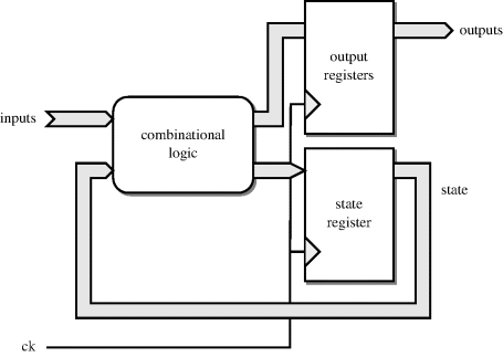
When encoding the outputs for this form, the one-cycle delay introduced by the output register needs to be allowed for in the design. So the signal assignments to the outputs must set the outputs a cycle (state) before they are required. In other words, they are arranged so they specify the value that the output will have after the state transition rather than the output for the current state.
The previous example using the single-process form of FSM is:
architecture behaviour of signature_detector is
type state_type is (start, found1, found0, detect);
signal state : state_type;
begin
-- register block
process
begin
wait until rising_edge(ck);
found <= '0';
case state is
when start =>
if d = '1' then
state <= found1;
else
state <= start;
end if;
when found1 =>
if d = '0' then
state <= found0;
else
state <= found1;
end if;
when found0 =>
if d = '1' then
state <= detect;
found <= '1';
else
state <= start;
end if;
when detect =>
if d = '1' then
state <= found1;
else
state <= found0;
end if;
end case;
end process;
end;
Note how the found signal is set to ‘0’ by default, but this assignment is overridden by ‘1’ in the case where the next state is detect.
This style of state machine is difficult to program because of this need to think one state ahead, but it does have registered outputs that are therefore available immediately after the clock and are guaranteed to be glitch-free.
12.2.4 State Encoding
FSM inference: is automatic and FSM synthesis will choose the most efficient encoding for the state. However, sometimes you want to specify the encoding. Some synthesisers allow the user to specify the binary encoding of the state values. This usually allows a predefined sequence to be specified, such as one-hot encoding or sequential encoding (0, 1, 2…). Alternatively, the actual binary encodings can be specified. Some synthesisers will not support user-customisation at all, in which case the encoding will be automati-cally selected.
Unfortunately, the way you specify the state encoding is completely synthesiser-specific so you have to see the synthesiser's manual to determine how to do it. Typically it is either an attribute in the VHDL file or it is a project setting in a settings file. Here's an example of the use of an attribute:
signal state : state_type;
attribute fsm_encoding : string;
attribute fsm_encoding of state : signal is "one_hot";
This is a completely made-up attribute – the real name and value will be different in practice and you can only find out what it is from the synthesiser's manual.
In the absence of an explicit encoding, the synthesiser will allocate states automatically. This is usually sufficient and it is rarely necessary to choose an encoding.
12.2.5 Illegal States and Resets
An FSM in VHDL uses an enumeration type that probably will not have exactly a power of two values. When it is mapped onto logic, there will be some state encodings that do not correspond to a state. These are known as illegal states.
Even if the enumeration does have a power of two values, the FSM synthesis may choose one-hot encoding that has one register per state and therefore for S states in the RTL model, has 2S possible states in the hardware, of which all but S are illegal.
If an FSM gets into an illegal state, it may get stuck there since the FSM synthesis does not allow for this possibility – the optimisation of the next-state logic does not account for the illegal states. Indeed, doing so would make one-hot encoding the least effective encoding, whereas it is often (particularly for register-rich FPGA technologies) the best encoding.
Illegal states are not due to erroneous synthesis, they are due to the power-up behaviour of hardware, so it is not the job of FSM synthesis to solve this problem, it is a design issue. The only time an FSM can get into an illegal state is at power-up when the initial state cannot be controlled. Once the FSM is in a legal state, it will always stay in legal states because the FSM synthesis will ensure this. So, in order to avoid illegal states, all that is necessary is to make the FSM resettable. By resetting to a legal state after power-up, the problem of illegal states is solved.
A reset can easily be added to the register part of the template and has no effect on the combinational part. For example, using the two-process, one-decoder FSM model, a synchronous reset to the start state could be incorporated by adding a reset input to the entity and rewriting the register part.
-- register block
process
begin
wait until rising_edge(ck);
if rst = '1' then
state <= start;
else
state <= next_state;
end if;
end process;
This is a synchronous reset. As usual, an asynchronous reset could be used if that is the design requirement. However, the general rule as explained in Section 9.9 is to use synchronous reset unless there is a compelling reason not to.
Conceptually a register bank is not the same as a RAM, since a register bank is a 2-dimensional array of flip-flops and a RAM is a two-dimensional array of memory cells. However, this is an implementation difference and at the level of abstraction used for RTL design, there is no difference. For this reason, the two structures will be discussed together.
The two structures will be referred to collectively as memories, so this term will be used wherever the discussion applies to both structures. The terms RAM and register-bank will then be used to distinguish between the two types of memory.
A memory is generated by using the register model from Chapter 9 on an array signal to create an array of registers. Each element of the array can then be accessed by array indexing. The element type for a register bank can be any synthesisable type, such as any of the synthesis types described in Chapter 6. You could for example have a memory made of an array of float. However, if a RAM is required it is usually necessary to only use arrays of std_logic_vector.
RAMs are then inferred from the memory model by the synthesiser, so to get a RAM, you must use one of the RAM inference templates. This inference decision is based partly on the functionality available in the target technology and partly on the size of the memory: small memories are more efficiently implemented as register banks, whereas larger memories are more efficiently implemented as RAMs.
The problem with RAM inference is that the templates can vary from technology to technology – one technology may implement a particular type of RAM, whilst another does not. If you use a template that's not supported by the technology, the memory will be implemented as a register bank. So if you want a RAM, it is really important to check the documentation to see which templates are available to use with your target synthesiser/technology combination and to check the synthesis tool's log to ensure that the mapping has taken place.
In the following three sub-sections, three different memory models will be explained. The memory models will be illustrated by examples that will be written as generic components. The data inputs, outputs and the memory itself must be std_logic_vector to get a RAM. The address is an unsigned number designating the offset into the array of words, so type unsigned is used to represent it.
The three different versions reflect different behaviour on read: synchronous or asynchronous, and different behaviour on a write: whether to read the previous value of a word while writing the new value – conceptually a read-before-write; or whether to read the new value as it is written – conceptually a write-before-read.
In each example, the memory will be parameterised for both word size (word_size) and the size of the address bus (address_size). The number of words in the register bank will be the full set of addressable words for the address bus size – namely 2address_size. The interface is the same for all of the examples except for the entity name so that the differences in the models is more obvious.
library ieee;
use ieee.std_logic_1164.all;
use ieee.numeric_std.all;
entity RAM is
generic (word_size : natural;
address_size : natural);
port (d : in std_logic_vector(word_size-1 downto 0);
ck : in std_logic;
write : in std_logic;
address : in unsigned(address_size-1 downto 0);
q : out std_logic_vector(word_size-1 downto 0));
end;
Note how the ports have been sized by the generic parameters.
12.3.1 Asynchronous Read, Synchronous Write
This version of the model implements a memory where the read and write operations are independent, such that the read is combinational (i.e. asynchronous) and the write is synchronous. This means that if you read and write to the same address, the read output will change as the write operation updates the memory contents.
The architecture is:
architecture behaviour of RAM is
type memory_type is array (0 to 2**address_size-1) of
std_logic_vector(word_size-1 downto 0);
signal memory : memory_type;
begin
-- write
process
begin
wait until rising_edge(ck);
if write = '1' then
memory(to_integer(address)) <= d;
end if;
end process;
-- read
q <= memory(to_integer(address));
end;
The main complication in writing the architecture is that the address bus is represented as an array, in this case a signal of type unsigned. This address is supposed to be used to index an array of registers, but it is illegal in VHDL to use an array type to index another array type – a scalar type such as integer must be used. The solution is to use a type-conversion function to convert the address bus into an integer value at the point of use; the return value of this function can then be used as an array index. Type conversions do not generate any hardware, so there is no synthesis overhead to this solution although there is a slight simulation overhead. In this case the to_integer function from package numeric_std will be used to perform the type conversion.
Note how the number of elements in the memory has been sized by the generic parameter address_size so that the full address range is covered. This has the advantage of making the memory simple – there are no out-of-range addresses for example. However, it is possible to use a third generic parameter to control the address range if an unconventional size is required, for example if the size is not a power of two.
The read assignment uses dynamic indexing of the source of the assignment: one of the elements of memory is selected and written to the output q. If a register bank is being generated then the read operation will be implemented as a multiplexer structure selecting one of the register outputs. If a RAM is being generated then it will be implemented as a memory read operation that is functionally equivalent. Note that the read is combinational so if the RAM contents change, the output will change.
The architecture also contains a process that uses the edge function template for a register as explained in Section 9.4. This implements the write behaviour of the memory. Any of the register templates could be used here. The write assignment uses dynamic indexing of the target of the assignment: one of the elements of memory is selected to receive the value on input d, provided the control signal write is enabled. The other elements preserve their values. The synthesiser implements this functionality by creating a register or memory for each element of signal memory, since all the elements of the signal are potentially assigned to in the process. If this is implemented as a register bank, then the dynamic indexing is implemented as a demultiplexer structure that can route the d input to any of the registers in the register bank. If it is implemented as a RAM, it will be implemented as a memory write operation that is functionally equivalent.
This is the simplest form of memory template. However, most real RAMs have synchronous read and write operations. For this reason, this model will nearly always be mapped onto a register bank instead of a RAM.
This template is the recommended form if you want a register bank, but not if you want a RAM. Templates that will be mapped onto RAMs are covered in the following sections.
12.3.2 Synchronous, Read Before Write
This version of the memory model implements a memory where read and write are synchronous and, during a write operation, the old value of a word is presented at the output port whilst the new value is being written to it.
The entity has the same interface as the previous example and only differs in name: RAM_RBW. The architecture is:
architecture behaviour of RAM_RBW is
type memory_type is array (0 to 2**address_size-1) of
std_logic_vector(word_size-1 downto 0);
signal memory : memory_type;
begin
process
begin
wait until rising_edge(ck);
-- read
q <= memory(to_integer(address));
-- write
if write = '1' then
memory(to_integer(address)) <= d;
end if;
end process;
end;
The architecture contains a single process that uses the edge function template for a register as before. Both the read and write operations occur in the same process. Any of the register templates could be used here.
As in the previous example, the read assignment uses dynamic indexing of the source of the assignment: one of the elements of memory is selected and written to the output q. The difference is that it is now synchronous because the read takes place in a registered process. If a register bank is being generated then the read operation will be implemented as a multiplexer structure with a registered output. If a RAM is being generated then it will be implemented as a buffered memory read operation, which is functionally equivalent. Note that the read is reading the old value, not the new one, and holding it in an output buffer register. The positioning of the read first in the process is irrelevant and has been positioned there for clarity to the reader – in VHDL terms the reason this reads the old value is that memory is read a delta cycle before it is written.
The write assignment is identical to the previous example.
12.3.3 Synchronous, Write Before Read
This version of the memory model implements a memory where, during a write operation, the new value of a word is presented at the output port whilst the same value is being written to the memory. This is a slightly more complex memory design than the “Read Before Write” model and less likely to be available with every technology, but is still common.
The entity has the same interface as the previous example and only differs in name: RAM_WBR.
The architecture is:
architecture behaviour of RAM_WBR is
type memory_type is array (0 to 2**address_size-1) of
std_logic_vector(word_size-1 downto 0);
signal memory : memory_type;
signal read_address : unsigned(address'range);
begin
process
begin
wait until rising_edge(ck);
-- write
if write = '1' then
memory(to_integer(address)) <= d;
end if;
read_address <= address;
end process;
-- read
q <= memory(to_integer(read_address));
end;
The first part of the process implements the write operation in the same way as the previous example. However, also in this process is an assignment to an internal signal – read_address is a registered version of the address input.
In the concurrent signal assignment at the end of the architecture, the registered version of the address is used to index the memory in a read operation. In other words, the read is reading the value written in the previous clock cycle, by accessing the address specified in the previous clock cycle. This mimics the behaviour of a memory with synchronous output and write-before-read semantics, which is a common alternative form to the read-before-write on programmable devices. The synthesiser restructures this into a functionally equivalent output buffer.
If a register bank is being generated then the read operation will be implemented as a simple multiplexer structure with a registered output. If a RAM is being generated then it will be implemented as a buffered memory read operation, with bypass logic to handle the case where the same address is read and written at the same time, so the input value is fed to the output buffer directly at the same time as it is written to the RAM. It is this bypass logic that makes the write-before-read version larger and slower than the read-before-write.
12.3.4 RAM Read Optimisation
Many designs do not need simultaneous read and write but keep reads and writes as separate operations on different cycles. Some synthesisers allow you to optimise RAM inference by specifying that you do not require simultaneous read and write. This will enable the synthesiser to pick the smallest and probably also the fastest RAM implementation from the target technology regardless of which memory model you used in the design.
Specifying non-overlapping read and write may also enable RAM inference to take place where otherwise the memory would be implemented as a register bank.
Unfortunately, the way you specify this is completely synthesiser-specific so you have to see the synthesiser's manual to determine how to do it. Typically it is either an attribute in the VHDL file or it is a project setting in a settings file. Here's an example of the use of an attribute:
signal memory : memory_type;
attribute ram_type : string;
attribute ram_type of memory : signal is "no_rw_overlap";
This is a completely made-up attribute – the real name and value will be different in practice.
12.3.5 Getting a Register Bank
Sometimes you do just want a register bank, in which case you need to disable RAM inferencing.
Like all other synthesis options, the way you disable RAM inferencing is completely synthesiser-specific so you have to see the synthesiser's manual to determine how to do it. Typically it is either an attribute in the VHDL file or it is a project setting in a settings file. Here's an example of the use of an attribute:
signal memory : memory_type;
attribute ram_type : string;
attribute ram_type of memory : signal is "registers";
This is a completely made-up attribute – the real name and value will be different in practice.
12.3.6 Resets
You cannot use either asynchronous nor synchronous resets in memory models where a RAM is required, since RAMs do not generally have this functionality. So only the non-resettable register templates will result in RAM inference taking place.
If you want to be able to reset a RAM, then implement the reset at a higher level in the design as a series of writes of the reset value to all addresses. Do not be tempted to build this functionality into the RAM architecture, this may disable the RAM inference algorithm and result in a register bank instead.
A register bank, by contrast, can have either type of reset because it is just an addressable array of ordinary registers as described in Chapter 9.
A ROM is another structure inferred by the synthesiser so you need to use a specific template to get ROM inference. Furthermore, if the target technology does not support ROMs, or the synthesiser cannot implement a ROM that meets the design requirements, then it will be implemented as decoding logic instead. In FPGAs, the basic logic element is effectively a ROM already, so very efficient mappings can be achieved by using ROM models.
The difference with ROMs compared with RAMs is that you cannot design a generic ROM and then reuse it wherever you need it, for the simple reason that each ROM will have different data contents and the contents are hard-coded into the design. Thus, for every ROM in the design you need to design a different entity and architecture using the same ROM template.
Note: it is recommended practice to separate the ROM into its own design unit, having a separate entity and architecture, rather than mixing it up with the rest of the design. This is more likely to result in ROM inference taking place and some synthesis tools require it.
12.4.1 Case Statement Decoder
The most common ROM template uses a case statement to decode all possible values of the ROM's address, mapping each value onto a signal assignment where the target is the same signal and the source is a constant value.
For example, here's a decoder from 3-bit Gray code to binary using a ROM template:
library ieee;
use ieee.std_logic_1164.all;
use ieee.numeric_std.all;
entity gray_decode is
port (gray : in std_logic_vector(2 downto 0);
binary : out unsigned(2 downto 0));
end;
architecture behaviour of gray_decode is
begin
process(gray)
begin
case gray is
when "000" => binary <= "000";
when "001" => binary <= "001";
when "011" => binary <= "010";
when "010" => binary <= "011";
when "110" => binary <= "100";
when "111" => binary <= "101";
when "101" => binary <= "110";
when "100" => binary <= "111";
when others => binary <= "XXX";
end case;
end process;
end;
Note how the when others clause is used to set the output to unknown during simulation. This is required by simulation because there are many input permutations with metalogical values not covered by the other cases. This value will be ignored in synthesis because the case statement is regarded as complete with all the real input encodings covered.
12.4.2 Table Lookup Decoder
There is also a table lookup style of ROM that can be simpler and more compact, especially suitable where the input encoding is numeric. This can be applied to the reverse encoding from binary to gray code since the binary value is a numeric type:
library ieee;
use ieee.std_logic_1164.all;
use ieee.numeric_std.all;
entity gray_encode is
port (binary : in unsigned(2 downto 0);
gray : out std_logic_vector(2 downto 0));
end;
architecture behaviour of gray_encode is
type memory_type is array (0 to 7) of
std_logic_vector(2 downto 0);
constant memory : memory_type :=
("000", "001", "011", "010", "110", "111", "101", "100");
begin
gray <= memory(to_integer(binary));
end;
The possible output values are stored in a constant array such that the offset in the array of each output value is equal to the input address that selects it, in this case the input port binary. This might be clearer if the explicit form of the aggregate is used in the initial values of the constant:
constant memory : memory_type :=
(0 => "000",
1 => "001",
2 => "011",
3 => "010",
4 => "110",
5 => "111",
6 => "101",
7 => "100");
Because of the restriction in VHDL that arrays types such as unsigned cannot be used to index arrays, the array type has to be declared with a natural range, which is also why the offsets into the aggregate are expressed as integer values rather than as bit-strings. The input signal binary is type-converted to natural using the to_integer function and then the result used to index the array.