Multi-bit NAND Flash memories for ultra high density storage devices
R. Micheloni and L. Crippa, PMC-Sierra, Italy
Abstract:
This chapter is about NAND Flash memories, which have outpaced DRAMs in the technology scaling race. The first part of this work is devoted to the basics of this technology, including array architectures and operations (read, program and erase). Multi-bit per cell approaches (MLC and TLC) are also described, because they strongly drive the price reduction at the cost of reduced reliability. Lastly, the new 3D approach is introduced: the industry is still in a development phase, and here we present a summary of the pros and cons of the most promising candidates.
Key words
NAND Flash; MLC; TLC; charge trap; 3D array
3.1 Introduction
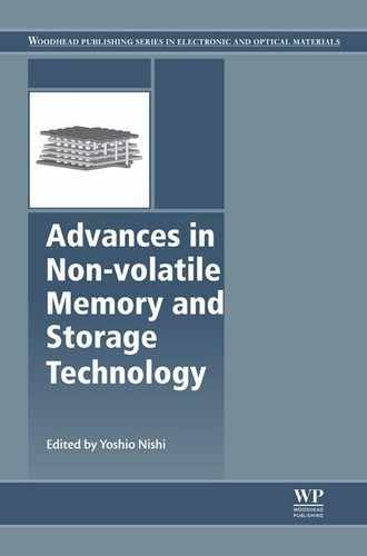
Where other semiconductor memories were on a 2-year cadence for new process technology introduction, NAND Flash memories have historically been on a 1-year cadence. In 2005 this accelerated process scaling resulted in a bit size of SLC NAND, overtaking MLC NOR. MLC NAND is by far the lowest-cost semiconductor memory, with none of the memory technologies even close to being cost competitive. This is mainly due to the very small cell size combined with multi-level cell capability (Fig. 3.1).
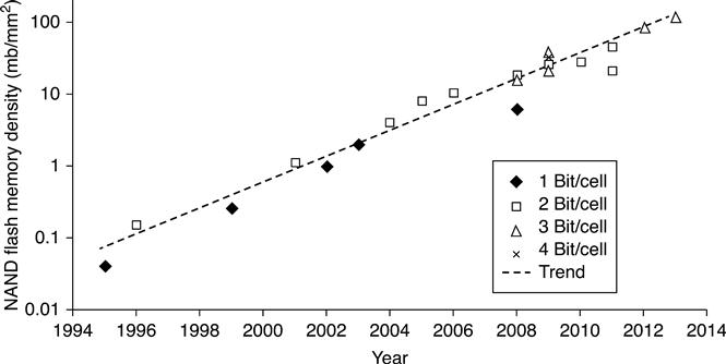
Figure 3.2 illustrates the concept of multi-level cell storage in Flash memories. Conventional SLC or single-level cell storage distinguishes between a ‘1’ and ‘0’ by having no charge or charge present on the floating gate of the Flash memory cell. By increasing the number voltage threshold (VTH) levels, more than one bit per cell may be stored. Two bits per cell (MLC) storage is enabled by increasing the number of VTH levels to four. Similarly, by increasing the number of levels to 8 and 16, 3 b/cell per cell (8LC or TLC) and 4 b/cell (16LC) storage is enabled.

The benefit of multi-level cell storage is that storage capacity may be increased without a corresponding increase in process complexity. The same fab (chip fabrication plant) equipment used to manufacture silicon wafers for SLC products may be used to manufacture MLC. However, multi-level cell storage requires accurate placement of the VTH levels so that they do not overlap. As the number of VTH levels increases, the time it takes for accurate programming and sensing increases. Additional circuitry and programming algorithms are necessary to compensate for the degradation of the performance and endurance of such devices. However, transitioning from SLC to MLC, to 3-bit per cell and to 4-bit per cell technology is equivalent to shrinking the process technology, without additional capital investment.
The first MLC NAND was introduced at the end of 2001 by SanDisk and Toshiba. It was a 1 Gb chip based on 0.16 μm process technology.1 The first commercial production of 8LC began in 2008, again by SanDisk and Toshiba. The device, a 16Gb product based on 56 nm process technology2 was introduced as a process technology one generation behind the mainstream MLC products. As a result, the device was short-lived, since the MLC products based on 43 nm technology were more cost-competitive than the 8LC product.
16LC was introduced in 2009 on a mature process technology – 43 nm.3. Note that the cost per bit reduction becomes progressively smaller as we transition from SLC to 16LC. An approximate 40 to 50% reduction can be obtained by moving from SLC to MLC, but this figure drops to 20% for MLC to 8LC, and 10% for 8LC to 16LC. As a result, the economic benefit of 16LC may not be enough to justify the additional design efforts to implement it.
3.2 Array architectures
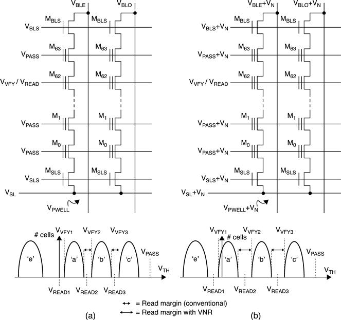
In the NAND array, memory cells are connected in series, in groups (strings) of 2k cells, up to 64 or 128 (Fig 3.3).4–7 MBLS and MSLS NMOS selector transistors connect the string to bit line (BL) and to source line (SL) respectively.
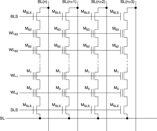
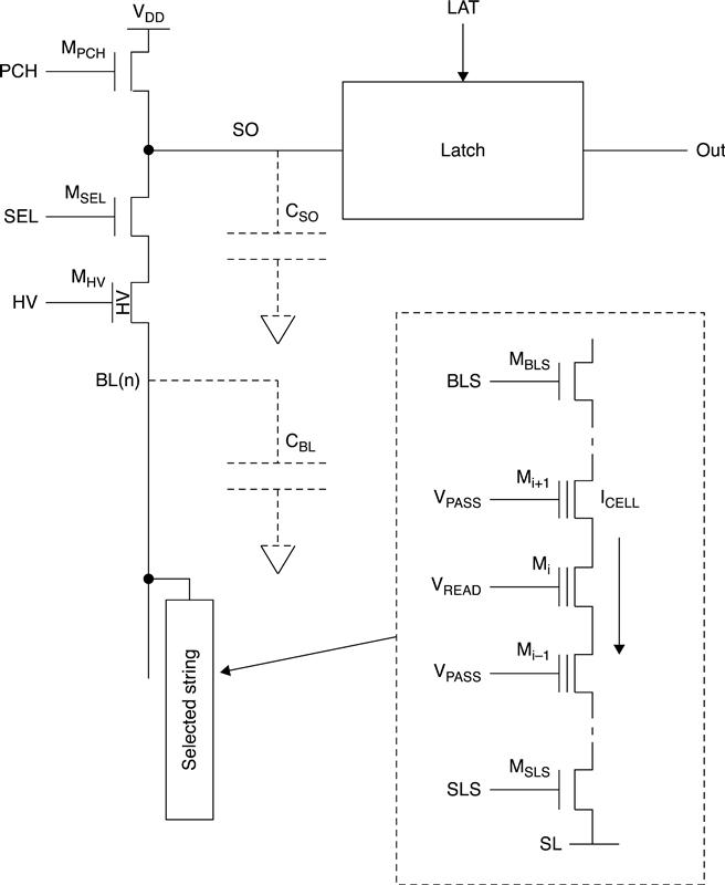
A typical block diagram of a NAND Flash memory is shown in Fig. 3.4. The row decoder controls the string select lines and the word lines of each block. Sense amplifiers (SAs) are connected to the bit lines, and the peripheral circuits manage data input/output during read/write operations.
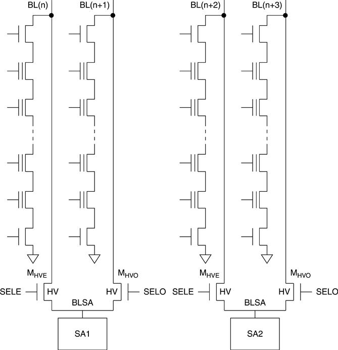
There are two possible memory architectures: Even/Odd Bit Line architecture (EOBL) and All Bit line Architecture (ABL). In the EOBL, one sense amplifier is shared between 2 bit lines (Fig. 3.5).8,10,12,14–19,21,23,24 MHVE MHVO (high-voltage, even and odd transistors, respectively) act as a multiplexer; when even (odd) bit lines are selected, odd (even) are unselected. Also a two-side page buffer interleaving architecture exists, where the even/odd bit line pair ends alternatively in the up and down selectors.1,9,11,13,15
In the ABL architecture there is a sense amplifier for every BL. As a consequence, ABL doubles the number of sense amplifiers with respect to EOBL. Sense amplifi ers are typically located on both sides of the cell array (Fig. 3.6(a))2,3,20,22 and this directly results in increased chip size. In fact, to supply stable core power to the top SAs, which are located at a long distance from power pads, wide power buses are necessary. Furthermore, signal delay due to the long distance between top SAs and I/O pads significantly degrade DDR interface performance. Having the SA on one side has some advantages, such as power line area reduction and a faster data path. On the other hand, having a one-sided ABL architecture causes severe lithographic challenges (Fig. 3.6(b)).
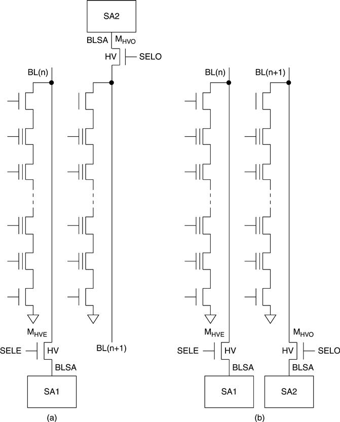
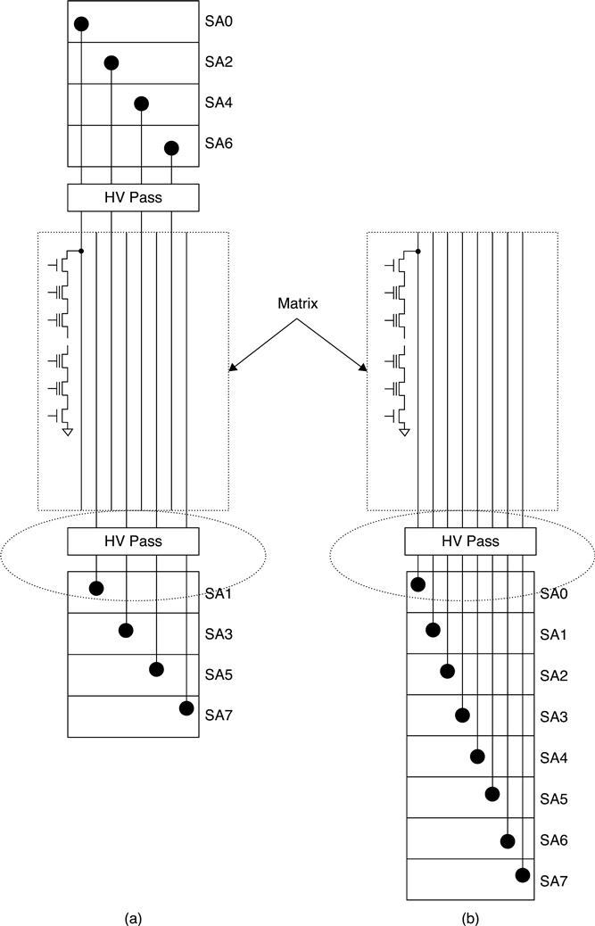
Figure 3.7 shows the layout architecture of one-side and two-side ABL. It is important to take care of the layout density of the signals in the circled area. In particular, BLSA signals in the one-sided sense amplifier structure need the same metal pitch as the bit lines inside the array.25 Alternatively, the density can be reduced by using another core metal as a bridge connection.26
ABL has some advantages over EOBL, because read and program operations are execuated in parallel on all bit lines (there is no concept of even/off).4 As a result, the power consumption is reduced, together with program and read disturbs. Another benefit of the parallel program operation is the cell-to-cell floating gate interference reduction. As always, there are also some drawbacks: in order to understand them, the reader is encouraged to follow the deep dive on current techniques described in the following section.
3.3 Read techniques
As for other types of Flash memories, in NAND the stored information is associated with the cell’s threshold voltage VTH: in Fig. 3.8 the threshold voltage distributions of cells containing one logic bit are shown. Flash cells act like usual MOS transistors. Given a fixed gate voltage, the cell current is a function of its threshold voltage. Therefore, through a current measure, it is possible to understand which VTH distribution the memory cell belongs to.

The fact that a memory cell is part of a string made of several cells causes some issues. First of all, the unselected memory cells must be biased in such a way that their VTH voltages do not affect the current of the addressed cell. In other words, the unselected cells must behave as pass-transistors. As a result, their gate must be driven to a voltage (commonly known as VPASS) higher than the maximum possible VTH. In Fig. 3.8, VPASS has to be higher than VTHMAX. However, the presence of 2n − 1 transistor in series has a limiting effect (saturation) on the current’s maximum value.
The order of magnitude of the cell current, in state-of-the-art NAND technologies, is a few hundreds of nA (or even lower): this means a reading current of some tens of nA. Moreover, tens of thousands of strings are read in parallel, implying tens of thousands of sense amplifiers. Because of this, a single sense amplifier has to guarantee a full functionality with a very low number of transistors.
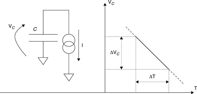
The reading method of the Flash NAND memories is basically an integration of the cell current on a capacitor in a fi xed time (Fig. 3.9). The voltage ΔVC across a capacitor C, charged by a constant current I for a time period ΔT, is described by the following:
[3.1]
Since the cell current is related to its VTH, the final voltage on the capacitor is also a function of VTH. Usually, the integration capacitor is the bit line parasitic capacitor;8–10 recently, integration over a little dedicated capacitor has become popular, because it allows faster access times. The above-mentioned techniques can be used both in SLC and MLC NAND memories. In the MLC case, multiple basic reading operations are performed at different gate voltages.
In Fig. 3.10, the basic integration scheme is shown, where VPRE is a constant voltage. At the beginning, CBL is charged up to VPRE and then is left floating (T0). At T1 the string starts sinking current (ICELL) from the bit line capacitor and the cell gate is biased at VREAD. If the cell is erased, the sunk current is higher than the current IERAMIN. A programmed cell sinks a current lower than IERAMIN (it can also be equal to zero). CBL is connected to a sensing element (comparator) with a trigger voltage VTHC equal to VSEN. Since IERAMIN, CBL, VPRE and VSEN are known, it follows that the shortest time (TEVAL) to discharge the bit line capacitor is
[3.2]
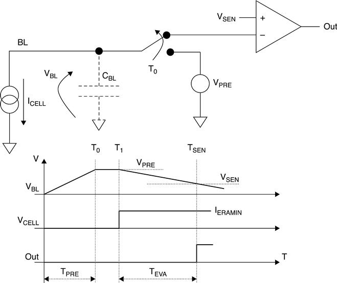
If the cell belongs to the written distribution, the bit line capacitor is not discharged below VSEN during TEVAL. As a result, the output node (OUT) of the voltage comparator remains at 0. Otherwise, if the cell is erased, VBL drops below VSEN and the OUT signal is set to 1. The basic sense amplifier structure is sketched in Fig. 3.11. During the pre-charge phase, TPRE, MSEL and MPCH are biased to VPRE and VDD + VTHN, respectively. VTHN is the threshold voltage of a NMOS transistor and VDD is the device’s power supply voltage. As a consequence, CBL is charged to the following value:
[3.3]
During this phase, the SO node charges up to VDD. Since VGS and VDS can be higher than 20 to 22 V, MHV has to be a high voltage (HV) transistor. In fact, during the erase phase, the bit lines are at about 20 V and MHV acts as a protection element for the sense amplifier’s low voltage components. Instead, during the reading phase, MHV is biased at a voltage that makes it behave like a pass-transistor. Moreover, during the pre-charge phase, the appropriate VREAD and VPASS are applied to the string. MBLS is biased to a voltage (generally VDD) that makes it work as a pass transistor, while M SLS is turned off in order to avoid cross-current consumption through the string.
Typically, VBL is around 1 V. From Eq. 3.3, VPRE values are shown as approximately 1.4 to 1.9 V, depending on the VTHN (NMOS threshold voltage). The bit line pre-charge phase usually lasts 5 to 10 μs, and depends on many factors, above all the value of the distributed bit line parasitic RC. Sometimes this pre-charge phase is intentionally slowed down to avoid high current peaks from VDD. In order to achieve this, the MPCH gate could be biased with a voltage ramp from GND to VDD + VTHN.
At the end of the pre-charge phase, PCH and SEL are switched to 0. As a consequence, the bit line and the SO node are left floating to a voltage (VPRE − VTHN) and VDD, respectively. MSL is then activated, and the string is enabled to sink (or not) current from the bit line capacitor. At this point, the evaluation phase starts. If the cell has a VTH higher than VREAD, no current flows and the bit line capacitor maintains its pre-charged value. Otherwise, if the cell has a VTH lower than VREAD, the current flows and the bit line gets discharged.
Let us now move to reading techniques with time-constant bit line biasing, i.e. the bit line voltage is forced to a constant value during the evaluation phase. This time, a dedicated capacitor is used instead of the CBL bit line parasitic capacitor. This technique is usually combined with ABL. Figure 3.12 shows the main elements of the ABL sense amplifier. The sense amplifier latch is replaced by a voltage comparator with a VTHSA trigger voltage. The other elements remain the same as those used with EOBL, but they are used in a different way. The capacitor CSO does the integration of the cell current: it can be made by using either MOS gates or poly-poly capacitors.
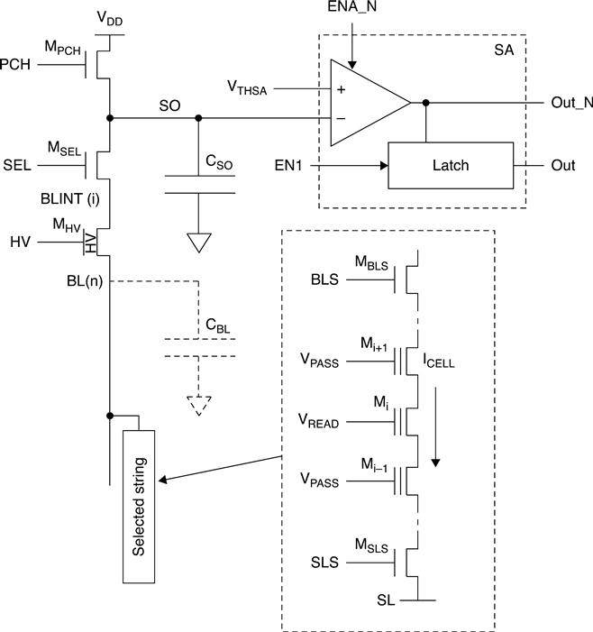
Figure 3.13 shows the main timings during read. As usual, during the precharge phase, MPCH and MSEL gates are biased to (VDD + VTHN) and VPRE, respectively. MHV, which is of high-voltage type, works as pass transistor. Also the signals which drive the string gates (VREAD, VPASS and BLS) are driven as before. Instead SLS signal is immediately activated in order to stabilize the bit lines during the pre-charge phase. In fact, if the SLS had been activated during the evaluation phase, there would have been a voltage drop on bit lines.

The pre-charge voltage can be written as
[3.4]
and is valid only for the bit lines that have an associated string in a non-conductive state. Equation 3.4 should be replaced by
[3.5]
where Δ is the voltage drop on the bit lines resistance; typical values are in the order of hundreds of kΩ up to one MΩ. NAND strings having deep erased cells might create voltage drops of a few hundreds of mV, but also cells absorbing tens of nA generate drops of tens of mV. By activating SLS during the evaluation phase, there would have been some noise on the adjacent bit lines due to the above-mentioned voltage drops. In this way, the voltage on the bit lines would no longer have been constant. Δ also includes the necessary MSEL overdrive. On the other hand, the connection of SLS during the pre-charge phase determines a significant current consumption.
At the end of the pre-charge phase (T1), the bit lines are biased to a constant voltage and VSO is equal to VDD. MPCH is switched off and the evaluation phase starts. Actually, MPCH is biased to a VSAFE voltage value. When MPCH is switched off, the cell current (through MPRE) discharges the CSO capacitor. If, during the evaluation time, VSO < VTHSA (trigger voltage of the comparator in Fig. 3.12), then the signal OUT_N switches (dotted lines in Fig. 3.13). The ‘threshold current’ IREADTH is defined as
[3.6]
where
[3.7]
Please observe that, because the bit line is biased to a fixed voltage, constant current flows. Therefore, it is possible to extrapolate the evaluation time:
[3.8]
Given the same read currents, it follows that the ratio between Eq. 3.2 and Eq. 3.8 is determined by the ratio between CBL and CSO. CBL is a parasitic element and has a value of 2 to 4 pF. Instead, CSO is a design element and has typical values around 20 to 40 fF, i.e. two orders of magnitude lower than CBL. The reduction of the evaluation time from 10 μs to hundreds of ns is another advantage of the ABL. Every read and verify operation of the programmed distributions are carried out by applying to the gate of the cell a VREAD voltage that is greater than (or equal to) zero. As a consequence, programmed distributions can only have positive VTH.
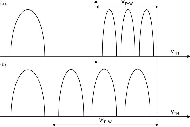
NAND technology does not allow the generation of negative voltages inside the memory chip. Therefore, negative VTH cannot be verified using the sensing methodologies described above. Methods to determine the position of the cells belonging to the erased distributions have been developed,4 enabling the extension of the programmed window VTHPW of Fig. 3.14(a) to V′THPW of Fig. 3.14(b). The main benefit is that either the distance between distributions can be increased (thus improving read margins) or the width of the distributions can be increased (thus improving programming speed).
Virtual Negative Read (VNR) technique was developed to read negative VTH without adding any process steps or mask.27 To read − VN, + VN is applied to P-well, BLs, select WLs (VREAD/VVFY) and unselected WLs (VPASS): this is equivalent to making a virtual shift of + VN (Fig. 3.15) in the negative direction. For example, by using VNR, the VVFY1 level can be lowered to maximize the distance from VVFY3, which means more margin for data retention.
3.4 Program and erase algorithms
VTH is modified by means of the Incremental Step Pulse Programming (ISPP) algorithm (Fig. 3.16): a voltage step, whose amplitude and duration are predefined, is applied to the gate of the cell. Afterwards, a verify operation is performed, in order to check whether VTHR has exceeded a predefined voltage value (VVFY). If the verify operation is successful, the cell has reached its final destination and is excluded from the following program pulses. Otherwise, another cycle of ISPP is applied to the cell, but this time the program voltage is incremented by ΔVpp.
During programming, all the cells on the same word line are biased at the same high voltage (because of the physical connection), but the program operation has to be bit selective. Therefore, there is a need for a mechanism to inhibit the electron injection, despite the high voltage on the gate. Basically, a high channel potential is created to reduce the voltage drop across the tunneling dielectric and prevent the electrons tunneling from the channel to the floating gate (Fig. 3.17(a)). In the first NAND devices, the channel was charged by applying 8 V to the bit lines of the program-inhibited NAND string. This method suffers from several disadvantages,28 especially power consumption and high stress on the oxide between adjacent bit lines. Less power consuming is the self boost program inhibiting scheme. By charging the string select lines and the bit lines connected to inhibited cells to Vcc, the select transistors are virtually diode connected (Fig. 3.17(b)). By raising the word line potential, the selected word line to Vpp and unselected word lines to Vppass, the channel potential is boosted by the parasitic capacitors.
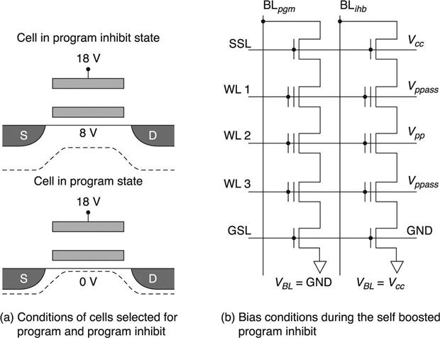
In fact, when the voltage of the channel exceeds Vcc − VTH,SSL, then SSL transistors are reverse biased and the channel of the NAND string becomes a floating node.
Two important disturbs occur during the program operation: Pass-disturb and Program-disturb (Fig. 3.18). The Pass-disturb affects cells belonging to the same string of the cell to be programmed. On the other hand, the Program-disturb affects cells that are not to be programmed and belong to the same word line as those that are to be programmed. The impact of this disturb is mainly due to the high voltages involved in the operation.
3.4.1 MLC program
If we take a block of NAND cells and apply just one program pulse, we can build what is called the ‘native’ VTH NAND distribution. This parameter is used to indicate the quality of a process technology: all NAND algorithms are developed to compress the native distribution. Figure 3.19 shows how the native distribution has been impacted by the technology shrink, for example, because of process variations such as random dopant fluctuation.29

Nowadays, multi-bit-per-cell storage is widely adopted in NAND memories. By dividing the available VTH window into more regions, 3-bit/cell21 or 4-bit/cell3 were developed. This approach is very valuable from a cost perspective, but implies a significant reduction of the distance between programmed states. Hence, a more accurate VTH control is required, which translates into more program pulses and verify operations: therefore, it is difficult to maintain the same program performances from one generation to another.
One of the biggest issues in narrowing distributions is the Floating Gate (FG) coupling among adjacent cells: this is basically caused by the parasitic capacitors in the physical array.
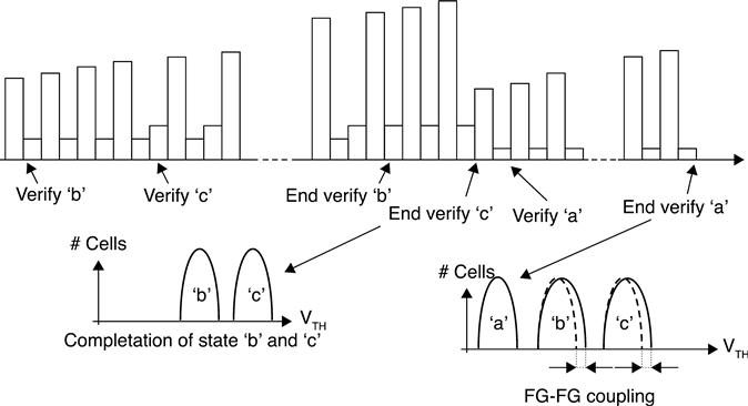
Generally speaking, in MLC NAND, the program operation shifts the cells from the erased state to states ‘a’, ‘b’ and ‘c’, by means of ISSPP30 (Fig. 3.20). At the beginning, only state ‘a’ is verified. When the ISSPP voltage reaches a certain level, ‘b’ verify starts. Of course, verify ‘a’ is still performed. When the program voltage is at a higher level, ‘c’ verify also starts, and all three verifies are performed one after the other. Once all the cells supposed to be in ‘a’ have reached their desired state, ‘a’ verify stops. At this point it is important to notice that when a cell has passed the verify operation, it will no longer be verified. Therefore, it suffers from program disturb and cell-to-cell coupling effect, caused by the neighbouring cells continuing their journey to ‘b’ and ‘c’; as a result, ‘a’ distribution is widened.

In the attempt to compensate for the above mentioned effect, the BCA algorithm was proposed as in.25 Figure 3.21 explains the concept: ‘b’ and ‘c’ are programmed first. The starting voltage is higher than the one used in the conventional approach. At the beginning, only ‘b’ is verified: at a higher voltage, ‘b’ and ‘c’ are verified. Once ‘c’ cells programming is completed, ‘a’ programming starts. In this way, distribution ‘a’ is not affected by ‘b’ and ‘c’ programming. It is worth mentioning that ‘b’ and ‘c’ distributions are not affected by ‘a’ programming, because ‘a’ is placed at a lower level.
However, CBA is slower because ‘a’ is treated as a separate entity and some of the program pulses are repeated twice. Due to the fact that ‘a’ becomes tighter, ‘b’ and ‘c’ can be a little wider, allowing a higher voltage step, thus reducing the overall time; but this goes back to reliability. All in all, the VTH budget has to be carefully optimized.
3.4.2 TLC program
In sub-30 nm technology, especially with TLC, a multiple-step programming scheme is generally adopted. 3,4 Figure 3.22 shows VTH distributions after each programming step. Before performing the following ISSPP step on a specific WL, adjacent WLs are programmed (Fig. 3.22(a)). The number in the bubble corresponds to the logical page number, and bottom-up (1, 2, 3, …) order has to be followed when writing the block. By shortening the VTH distance between adjacent word lines (Fig. 3.22b)), the coupling interference can be reduced.
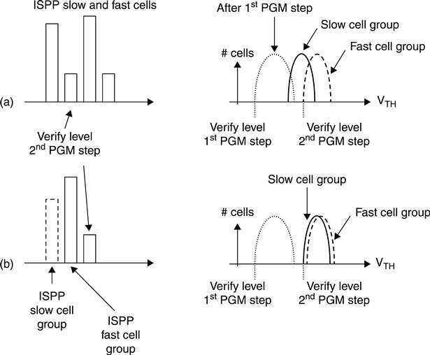
Adaptive multi-pulse program scheme (Fig. 3.23) has also been proposed.31 Basically, this algorithm takes into consideration the program speed of NAND cells.33 After the first program step, the VTH distribution is usually narrow. Because different cells have different program speeds, the ‘slow’ group reaches a lower VTH than the fast ‘one’. As a consequence, after the second step, the VTH distribution becomes wider (Fig. 3.23(a)). If different program voltages are applied to the two groups, the difference of VTH shift between them can be compensated for. Low level program bias is applied to the fast cell group, and high level program bias is applied to the slow cell group (Fig. 3.23(b)). Of course, the same concept can be extended to more groups.
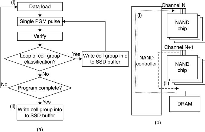
In order to implement this algorithm, cells must be classified during the first programming step and the basic idea is summarized in Fig. 3.24.33 Basically, a first program loop is carried out and cells are classified based on how many steps they need to reach a specific level. This information resides in the latches of the sense amplifiers and is fed to the external SSD controller. At this point, we are ready to perform the second programming operation, where program pulses are adjusted to the needs of each single speed group.
3.4.3 16LC program
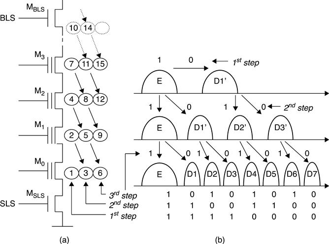
16LC programming is also based on a multi-phase program approach (Fig. 3.25).3,4 In the first round of M0, the cell is programmed MLC-like (Fig. 3.25b) in distributions DTj. Then the adjacent cell M1 is programmed MLC-like also (first round of M1). FG coupling effect on M0 due to programming of M1 is shown in Fig. 3.25b.
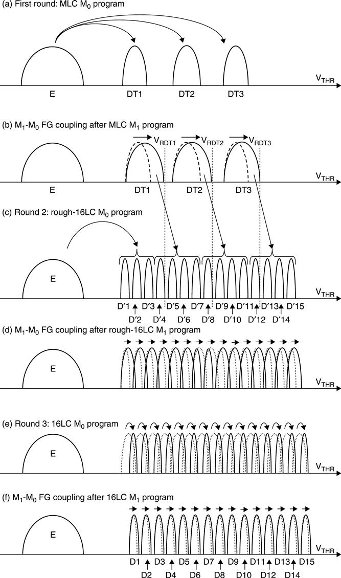
In the second round, cell M0 is roughly-programmed 16LC-like reprogramming distributions DTj into distributions Di (Fig 3.25(c)). Afterwards, the cells M2 and M1 are programmed MLC-like (first round of M2) and rough-16LC-like (second round of M1), respectively. Figure 3.25(d) shows FG coupling effect on M0 due to these two program operations.
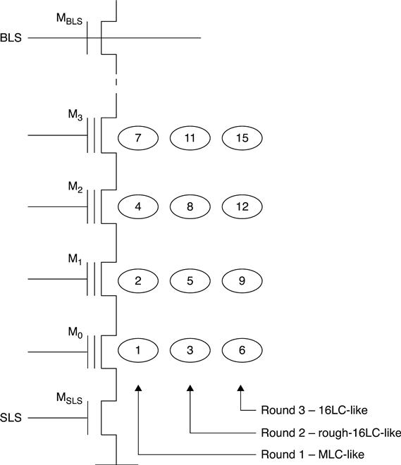
At this point, the third round of reprogramming of cell M0 (Fig. 3.25(e)) is performed at target levels Di. Such a final program is performed using a fine ΔISPP, 16LC-like. Then cells M3, M2 and M1 are reprogrammed 4LC-like (first round of M3), rough-16LC-like (second round of M2) and 16LC-like (third round of M1), respectively. Figure 3.25(f) shows the FG coupling effect on M0 due to these three program operations. The FG coupling effect on M0 is mainly due to the third round of reprogramming of the distributions of M1 from Di′ to Di: FG coupling on M0 is minimized. Figure 3.26 shows how this algorithm is mapped to the ABL architecture.
3.4.4 Erase
The erase operation resets the information of all the cells belonging to one block simultaneously. 4 Tables 3.1 and 3.2 summarize the erase voltages. During the erase pulse, all the word lines belonging to the selected block are kept at ground, the matrix ip-well must rise (through a staircase) to 23 V and all the other nodes are floating. This phase lasts almost a millisecond and it is the phase when the actual electrical erase takes place. Since the matrix ip-well (as well as the surrounding n-well) is common to all the blocks, it also reaches high voltages for the unselected blocks. In order to prevent an unintentional erase on those blocks, word lines are left floating; in this way, their voltage can rise due to the capacitive coupling between the word line layer and the underneath matrix layer. Of course, the voltage difference between word lines and ip-well should be low enough to avoid Fowler-Nordheim tunneling.
Table 3.1
Electrical erase pulse voltages for the selected block
| T0 | T1 | T2 | T3 | T4 | |
| BLeven | Float | Float | Float | Float | Float |
| BLodd | Float | Float | Float | Float | Float |
| DSL | Float | Float | Float | Float | Float |
| WLs | 0 V | 0 V | 0 V | 0 V | 0 V |
| SSL | Float | Float | Float | Float | Float |
| SL | Float | Float | Float | Float | Float |
| ip-well | 0 V | VERASE | VERASE | 0 V | 0 V |
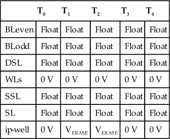
Table 3.2
Electrical erase pulse voltages for unselected blocks
| T0 | T1 | T2 | T3 | T4 | |
| BLeven | Float | Float | Float | Float | Float |
| BLodd | Float | Float | Float | Float | Float |
| DSL | Float | Float | Float | Float | Float |
| WLs | Float | Float | Float | Float | Float |
| SSL | Float | Float | Float | Float | Float |
| SL | Float | Float | Float | Float | Float |
| ip-well | 0 V | VERASE | VERASE | 0 V | 0 V |

After each erase pulse, an erase verify (EV) follows. During this phase all the word lines are kept at ground. The purpose is verifying if there are some cells that have a VTH higher than 0 V, so that another erase pulse can be applied. If EV is not successful for some columns of the block, there are some columns that are too programmed. If the maximum number of erase pulses is reached (typically 4), than the erase exits with a fail. Otherwise, the voltage applied to the matrix ip-well is incremented by ΔVE and another erase pulse follows.
3.5 Reliability issues in NAND Flash memory technologies
The memory reliability represents one of the major issues when scaling NAND technologies. The Flash memory cell is a metal-oxide-semiconductor device with a floating gate electrically isolated by means of a tunnel oxide and an interpoly oxide (Fig.3.27).34,35 Electrons transferred into the floating gate produce a threshold voltage variation of the associated transistor. Usually, silicon dioxide (SiO2) is used for tunnel oxides, and a stack of Oxide-Nitride-Oxide (SiO2-Si3N4-SiO2) for interpoly oxides.

In the last decade, attention was paid to the so-called charge trapping NAND memories, such as SONOS (Silicon-Oxide-Nitride-Oxide-Silicon) and TANOS (Tantalum-Aluminum-Nitride-Oxide-Silicon) as an alternative to floating gate. At the time of writing this chapter, floating gate is still the mainstream. The physical mechanism used for both injecting and extracting electrons to/from the floating gate is the Fowler-Nordheim (FN) tunneling.36 The high electrical field applied to the tunnel oxide (EOX ≈ 10 MV/cm) enables an electron to cross the thin insulator under the floating gate.
The endurance of a memory block is defined as the minimum number of Program/Erase cycles that the block can perform before leading to a failure. The erased and programmed distributions must be suitably separated in order to correctly read the logical state of a cell. The difference between EV (Erase reference Value) and PV (Program reference Value) is defined as the ‘read margin window’. However, keeping a correct read margin is not sufficient to guarantee a correct read operation: if during its lifetime the threshold voltage of an erased cell exceeds the EV limit and approaches 0 V, the current flowing through the cell may not be high enough to be identified as ‘erased’ by the reading circuitry, thus producing a read error. Similarly, a programmed cell could be read as ‘erased’ if its threshold voltage becomes lower than PV and approaches 0 V. As for the programmed distribution, it is also important that the upper threshold limit does not increase significantly with time, since a too high threshold can block the current flowing through the strings during reading operations.
FN tunneling leads intrinsically to oxide degradation.37 As a result of consecutive electron tunneling, traps are generated into the oxide.38 When filled by electrons, charged traps can increase the potential barrier, thus reducing the tunneling current.
Since the programming and erasing pulses feature constant amplitude and duration, less charge is transferred to and from the floating gate, causing an efficiency reduction of both the program and erase operations. A narrowing of the read margin window is then expected. Writing waveform optimization can help in limiting the trapped charge. For example, it has been shown that the window closure can be reduced by using low voltage erasing pulses able to remove the charge accumulated in the oxide.39
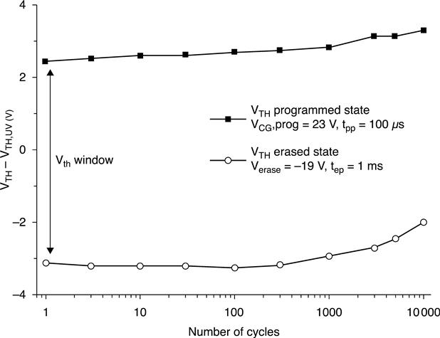
The retention concept is the ability of a memory to keep stored information over time, with no biases applied. Electron after electron charge loss could slowly lead to a read failure: a programmed cell can be read as erased if its VT shifts below 0 V. The intrinsic retention is mainly limited by tunneling through the oxide. Recent studies41 demonstrated that an oxide thickness of 4.5 nm is enough for granting theoretical intrinsic retention of 10 years. The cell retention worsens with memory cycling and this effect is appreciable as a reduction of the VTH levels (Fig. 3.29). Charge loss from the floating gate moves the VTH distribution towards lower values.
In additions, a tail in the lower part of the distribution indicates that a small percentage of cells are losing charge faster than average.
The rigid shift of the cumulative VT distribution can be related to the oxide degradation within the oxide and at the Si–SiO2 interface. In fact, an empty trap suitably positioned within the oxide can activate trap-assisted-tunneling mechanisms. Because of the reduced read margin, MLC shows more reliability issues. As a rule of thumb, a SLC can usually manage 50 to 100 k program-erase cycles, while MLC is limited to 3 to 10 k.35
The impact of the reliability effects related to the oxide degradation can be significantly reduced by using appropriate management policies. For instance, it is important to distribute the writing stress over the entire population of cells rather than on a single hot spot, thus avoiding that some blocks are updated continuously while the others keep unaltered their charge content. It is clear that blocks whose information is updated frequently are stressed with a large number of program-erase cycles. In order to keep the aging effects as uniform as possible, the number of both read and write cycles of each block must be monitored and stored by the memory controller. Wear Leveling techniques35,42 are based on a logical to physical translation for each sector. When the host application requires an update on the same logical sector, the memory controller dynamically maps the data on a different physical sector. The out-of-date copy of the sector is tagged as both invalid and eligible for erase. In this way, all the physical sectors are evenly used, thus reducing overall oxide aging.
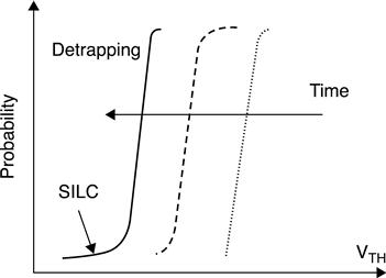
To reduce possible errors caused by oxide aging, Error Correcting Codes (ECC) are widely used in NAND memories.43 The array architecture itself may also affect the overall reliability: the most common effects are the so-called ‘disturbs’, i.e. the influence of an operation performed on a specific cell on its neighbors. Read disturb occurs when the same cell is read several times without erase operations in between. All the cells belonging to the same string of the cell to be read must be ON, independently of their stored charge. The relatively high Vpass applied on the control gate may trigger SILC effects: as a result, some cells suffer a positive VT shift. Since the SILC effect is not symmetrical, the cells affected by SILC are not necessarily the same that exhibit data retention problems. Figure 3.30 shows a typical read disturb configuration. Read disturbs do not cause permanent oxide damage.

For Pass-disturb and Program-disturb, please refer to Section 3.4. The Pass-disturb is similar to the read disturb, but is characterized by a higher Vpass, which enhances the electric field applied to the tunnel oxides and the probability of undesired charge transfer.
As the technology scaling of NAND Flash proceeds, emerging reliability threats such as the Gate-Induced Drain Leakage and the Random Telegraph Noise cannot be neglected. The Gate Induced Drain Leakage (GIDL) is a major leakage mechanism occurring in OFF MOS transistors when high voltages are applied to the Drain and it is attributed to tunneling taking place in the deep-depleted or even inverted region underneath the gate oxide.44
When the gate voltage in an nMOS transistor is 0 V (or below) and the Drain is biased at a high voltage, the n+ drain region under the gate can be depleted or even inverted. This effect causes a peak field increase leading to high field phenomena such as avalanche multiplication and band-to-band tunneling. As a result of these effects, minority carriers are emitted in the drain region underneath the gate and swept laterally to the substrate which is at a lower potential, thus completing a path for the leakage current.
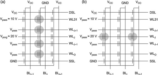
On NAND arrays the GIDL has been found to produce erroneous programming in specific cells,45 that is, those belonging to WL0, adjacent to the SSL transistor. The SSL transistor is OFF during programming and GIDL effects may be present if its drain is driven at high voltages. This situation occurs because of the self-boosting techniques adopted to prevent programming. As shown in Fig. 3.31, if WL0 is driven at Vpgm to program the cell in the central column, the channel voltage of the cells sharing the WL0 line are to be raised to prevent their programming. Because of the self-boosting technique, the source terminals of those cells (therefore also the drain node of their adjacent SSL transistors) are raised to values higher than VCC, thus leading to bias configurations activating GIDL effects. The electron-holes pair generation follows and the generated electrons are accelerated at the SSL-WL0 space region and can be injected as hot electrons in the floating gate of WL0 cells.

Recently, to mitigate GIDL effects, it has been proposed to introduce two dummy word lines to separate the two select transistors and the effective string of cells.46 To reduce the impact of these two additional word lines, longer strings of 64 cells have been proposed to improve area efficiency.
Since the 1950s, the Random Telegraph Noise (RTN) phenomenon has been observed in semiconductor transistors. The physical concept of RTN is attributed to a mechanism of capture/emission of single electrons by interfacial traps with time constants τc and τe, resulting in fluctuations of the transistor drain current and therefore on its threshold voltage (Fig. 3.32).47

RTN has been recently studied in NOR and NAND architectures.45,49 Figure 3.32 shows the cumulative distributions in a NAND array, where ΔVT has been calculated as the threshold voltage difference between two consecutive read operation.50 It can be observed that a ΔVT drift as far as the number of consecutive reading operation is increased. When increasing the number of program/erase cycles, new traps are created within the oxide and therefore VT instabilities are found to be increasingly probable.50 The previous results demonstrate that RTN must be considered when designing the ΔVT levels in multilevel architectures.
Another aspect to consider when scaling NAND is the discrete nature of the charge stored in the floating gate. The number of electrons determining the stored information continuously decreases with the tunneling area dimension. When only a few electrons control the cell state, their statistical fluctuations determine a non-negligible spread. These fluctuations may be attributed to the statistics ruling the electron injection into the floating gate during program or to the electron emission from the fl oating gate during erase or retention,51,52 both related to the granular nature of the current fl ow.53 A slight variation of the number of electrons injected during programming may produce VT variations, possibly leading to errors in MLC architectures.
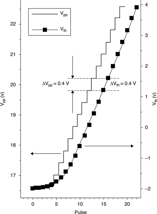
Cells in NAND MLC architectures are programmed by using a staircase voltage on the control gate. For sufficiently large step numbers, a linear VT increase is obtained, with a ΔVT per step almost equal to the applied voltage step (Fig. 3.33).
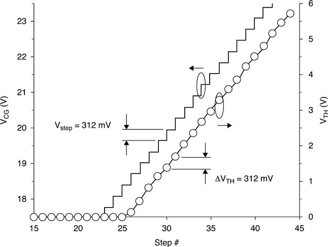
This is due to the programming current convergence toward an equilibrium stationary value, corresponding to an average number of electrons transferred to and from the floating gate for each step.54 The discrete nature of the charge flow introduces, for each cell, a statistical spread contribution to the resulting ΔVT after each step. It has been evidenced that the threshold voltage variation spread, indicated as σΔVt, depends only on the parameter Vstep of the programming waveform (i.e. on the injected charge per step qn) and not on the pulse duration and on the number of pulses to achieve ΔVT. The spread vs the average value of the threshold voltage variation shows a nearly Poissonian behavior for low ΔVT values, while sub-Poissonian statistics clearly appear for larger ΔVT.
3.6 Monolithic 3D integration
Market demand for higher capacity NAND Flash memories triggers continuous research.55 Unfortunately, physical barriers are expected to slow down the technology race. For instance, channel doping spread56 and random telegraph noise57 can induce large native threshold distributions, and electron injection statistics58 can cause additional variability after program, impacting both cell endurance and retention. Scaling string dimensions increase the electric field between word lines, leading to a higher failure rate. In the next decade, these and other limitations are expected to cause a drastic delay in the introduction of new planar technologies.
Three-dimensional monolithic integration represents an option for overcoming the bounds of actual planar devices.59 In recent years, the key players in the NAND industry have proposed several 3D architectures, trying to satisfy some basic requirements, such as a cheap process flow, reliable multi-level cell functionality, and compliance with current NAND device specification.
A fundamental change coupled to the evolution from planar to 3D memories is the transition from conventional floating gate (FG) to charge trap (CT) cells. Almost all NAND technologies in production use planar arrays with a polysilicon floating gate as storage element. Charge trap cells, which use dielectric material to store data, represent only an option for device scaling and cannot be considered the baseline process of planar arrays. On the contrary, almost all 3D architectures presented so far use charge trap cells because of their thinner stack (simpler integration).
3.6.1 Charge trap memories
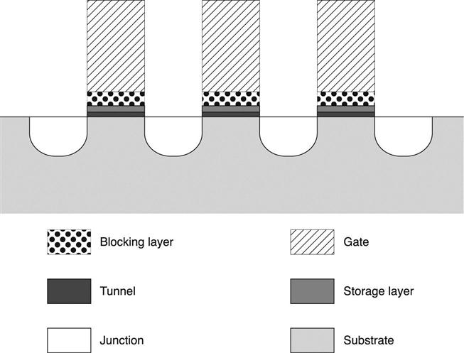
Both FG and CT VTH shift are determined by the number of elementary charges stored in the cell. The basic differences in the storage material are a semiconductor for FG and a dielectric for CT. Program and erase operations are impacted by the storage layer characteristics. CT memories often show a small working window due to saturation effects during write operations. Figure 3.34 shows the basic elements of a CT cell: gate, blocking layer, storage layer, tunnel layer and substrate.
Specific gate requirements depend on the architecture, but it is always important that the material in contact with the blocking dielectric has a high work function, in order to improve erase speed by limiting the parasitic back-tunneling current.
Silicon oxide and alumina are common blocking layers. Silicon oxide is preferred for architectures that need a limited thermal budget or a very thin stack (e.g. wrapped-around-gate), whereas alumina is used for cells that suffer for early erase saturation. Even if alternatives are available, silicon nitride is probably the best storage material, because it is characterized by a high trap density and by a giant lifetime of the charged state that ensure large threshold windows and excellent data retention.60
As in planar NAND, silicon oxide is the most common tunnel material; band engineered tunnel has been proposed61 only for architectures showing a very slow erase operation. We have to highlight the fact that 3D arrays have polycrystalline silicon substrates instead of silicon (i.e. in planar devices): this difference impacts cell performance, because of the limited electron mobility and increased diode leakage.
3.6.2 3D arrays
3D arrays can be classified according to their topology, which has a direct impact on cost, electrical performances and process integration. As we write, the most popular options are:
Array with horizontal channel and gate
As shown in Fig. 3.35, this array is obtained by stacking planar memories. Drain contacts and bit lines are shared, whereas all the other terminals (source, source selector, word lines and drain selector) can be decoded separately and independently. Since this 3D array is the natural evolution of the conventional planar array, this architecture was the first proposed. The main advantage of horizontal channel and gate architecture is the flexibility: each layer is built separately, removing many issues that are present with the other approaches (e.g. channel and junction doping). Process technology can be easily changed to let the cells work in either enhancement or depletion mode, but typically enhanced mode is preferred to easily reuse the know-how developed on planar memories.
From an electrical point of view, the largest difference compared to conventional memories is the floating substrate. As shown in Fig. 3.35, it is not possible to contact the body and this constraint impacts device operations (in particular erase). From an economic point of view, this approach is not very effective since it multiplies the costs to realize a planar array by the number of layers. The only improvement is represented by the sharing of the peripheral circuitry and metal interconnections. In order to limit wafer cost, the number of vertical layers must be as low as possible and, to compensate for this limitation, it is fundamental to use small cells. Many papers describing this array have been presented.62,63 Flexibility and easy reuse of the know-how developed in planar CT cell investigations are probably reasons to explain the remarkable activity in this area.
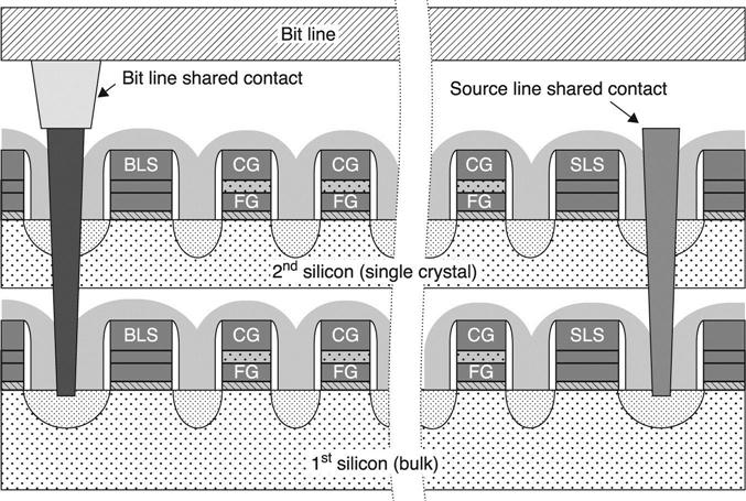
On the second silicon layer, the matrix MAT2 and all peripheral circuits are formed, while on the first layer we only find matrix MAT1 (Fig. 3.35). Main peripheral circuits are sensing amplifiers, source line (SL) and P-WELL voltage generators, and two NAND string decoders, one for each layer. Bit lines (BL) are only on the second layer and they are connected to MAT1 through the contacts shown in Fig. 3.35. Metal BLs are not present on MAT1; this is true also for SL and PWELL networks. Sensing circuits can access both MAT1 and MAT2; due to the fact that the bit line is shared, the capacitive load of a BL is comparable to that of a conventional planar device. Therefore, there is no penalty on power consumption and timing.
Thanks to the two independent string (row) decoders, a word line parasitic load is in the same range of a planar device. Furthermore, there are no additional program and read disturbs, because only one layer at a time is accessed.
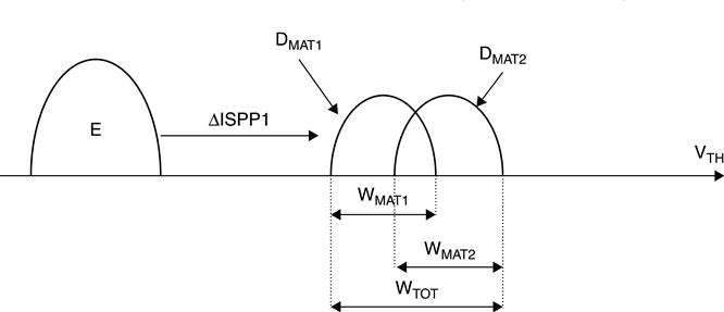
MAT1 and MAT2 are defined in different steps; as a consequence, the memory cell’s VTH distribution may be different. Figure 3.36 shows a typical VTH distribution after a single program pulse: two different distributions DMAT1 and DMAT2 are generated. In order to compensate for this, a dedicated programming scheme for each MAT layer is used.64 Depending on the specific MAT layer, program parameters such as VPGMSTART, ΔISPP and maximum number of ISPP steps, are properly chosen.
Array with vertical channel and horizontal gate
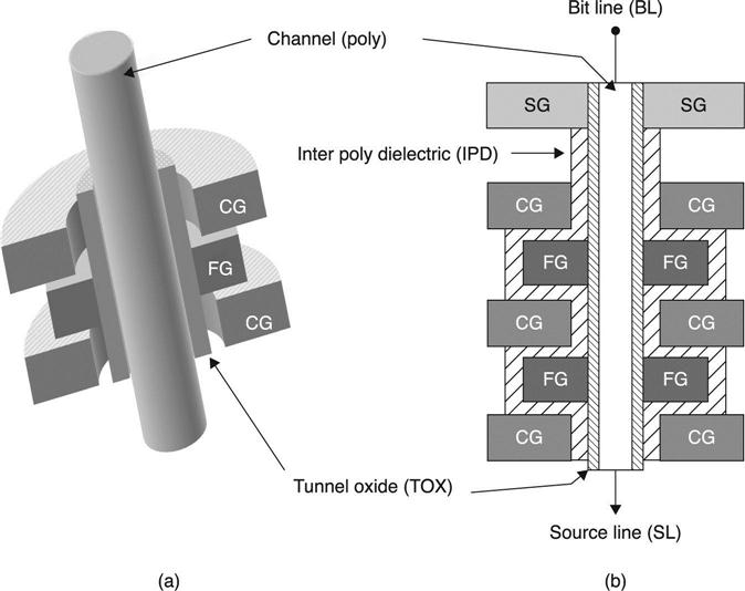
In this array, the number of critical masks is small, since the entire NAND stack is etched at the same time. Wafer cost is almost independent from the number of layers, but the typical cell size is relatively large and many layers are necessary to reach a small ‘equivalent’ cell area (i.e. single cell area divided by the number of layers).
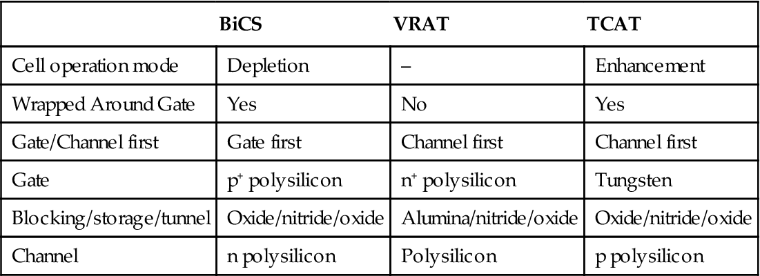
A typical cross-section is sketched in Fig. 3.37: the number of cells inside a string is defined by the number of stacked word lines. Bit lines and drain selector lines run horizontally and are used to select the NAND string. The three most important architectures with vertical channel and horizontal gate are BiCS,65 VRAT66 and TCAT.67 Table 3.3 is a summary of the most important characteristics of these arrays.
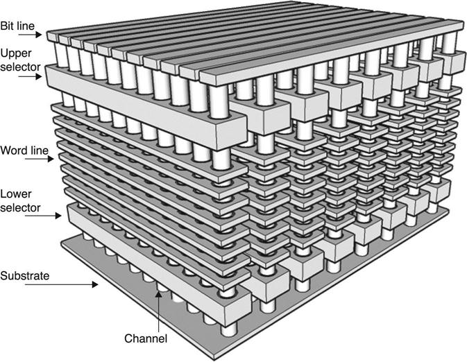
Table 3.3
Summary of the most important characteristics of 3D vertical channel arrays
| BiCS | VRAT | TCAT | |
| Cell operation mode | Depletion | – | Enhancement |
| Wrapped Around Gate | Yes | No | Yes |
| Gate/Channel first | Gate first | Channel first | Channel first |
| Gate | p+ polysilicon | n+ polysilicon | Tungsten |
| Blocking/storage/tunnel | Oxide/nitride/oxide | Alumina/nitride/oxide | Oxide/nitride/oxide |
| Channel | n polysilicon | Polysilicon | p polysilicon |
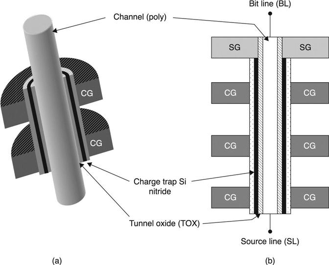
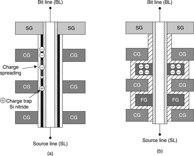
BiCS was proposed for the first time in 2007 and an improved version named P-BiCS [68] was presented in 2009 to improve retention, source selector performances and source line resistance. The most important characteristic of BiCS is the channel wrapped around by a CG gate (Fig. 3.38), which improves electrical performances.
VRAT is the only vertical channel cell with alumina as the blocking layer:69 this high dielectric constant material is supposed to compensate for the lack of a gate all around the channel.
TCAT is characterized by enhancement mode operation, a gate all around the channel, and the possibility to integrate a metal as the first gate layer. As in the VRAT case, the channel is deposited before the gate, and this choice could have beneficial effects on active dielectric quality, but the proposed flows need an extremely high conformity of active layers. It is worth mentioning that the electric field induced between adjacent cells accelerates the charge loss at high temperatures storage. TCAT and BiCS are compared in Fig. 3.39: TCAT has a biconcave structure, which contributes to the prevention of lateral charge losses.70
A 3D array with floating gate cells has been recently proposed, under the name Dual Control-gate with Surrounding Floating-gate (DC-SF).71–73 The DC-SF cell consists of a wrapped around floating gate with a dual control gate (Fig. 3.40).
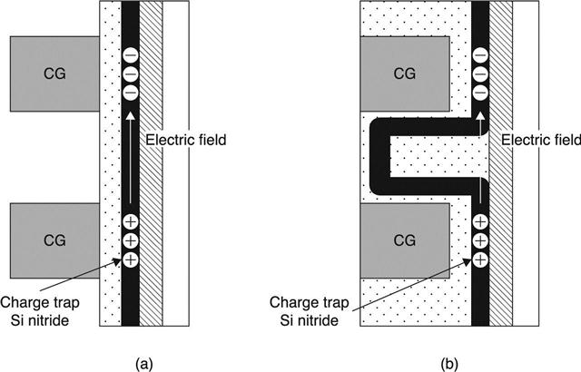
Vertical schematics of SONOS and DC-SF cells are compared in Fig. 3.41. The charge trap nitride layer in a SONOS string is continuously connected from top to bottom CGs along the channel side and acts as a charge spreading path (Fig. 3.41(a)), which is inevitably a limitation of the 3D SONOS cell. As a result, this causes degradation of data retention characteristics and poor definition of cell state. However, surrounding FG of Fig. 3.41(b) is completely isolated by IPD and tunnel oxide, implying that DC-SF is inherently more robust for isolating charges, thus preventing charge leakage.
3.7 Conclusion and future trends
The widespread use of NAND Flash memories in SSDs has unleashed new avenues of innovation for enterprise and client computing. System-wide architectural changes are required to make full use of the advantages of SSDs in terms of performance, reliability and power. Flash Signal Processing (FSP) technologies are becoming increasingly popular to countermeasure all the parasitic effects of a Flash NAND array. FSP does include a bunch of stuff already used in the communication environment: advanced ECCs such as LDPC codes, soft information management, data randomization and distribution coding engineering. In the coming years, industries and universities will have to focus on how to map all these techniques to the NAND architecture, together with the 3D challenges.