Developments in 3D-NAND Flash technology
R. Shirota, National Chiao Tung University, Taiwan
Abstract:
The market size of the NAND Flash memory has become around 20 billion US$ and has been increasing for the use of many applications, such as USB memory, embedded memory of mobile devices, SSD and so on. However, conventional 2D-NAND Flash memory has now reached its scaling limit of the cell. Thus, 3D-NAND Flash technology is now in strong demand. In this chapter, conventional 2D-NAND cell scaling issues are reviewed. Then, several kinds of cell structure and also device operation methods are reviewed. Finally, the operation margin issues of 3D-NAND Flash are overviewed.
Key words
NAND Flash memory; BiCS cell; TCAT cell; VG cell; SONOS memory
2.1 Introduction
Devices such as media tablets and smartphones are continually demanding higher capacity and more inexpensive ways to store content such as pictures, music and videos. NAND Flash manufacturers have traditionally used miniaturization to achieve this goal, but conventional technologies have reached their limit, whereas 3D manufacturing processes allow increasing density by layering NAND Flash cells on top of each other – providing a cost-effective way to use existing manufacturing equipment and expertise. This chapter describes the current state-of-the-art in 3D-NAND Flash memory design. The scaling limitations of 2D-NAND Flash memory are outlined. The use of vertical-channel and horizontal-channel cell configurations is described in detail – including structure, process and integration of different cell types, their program-erase-read operation, and specification. A final section covers the performance and electrical characteristics of different 3D-NAND Flash memory designs.
2.2 2D-NAND Flash memory: limitations in scaling
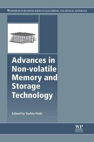
Conventional 2D-NAND Flash memory has reached its geometric scaling limit in the same way as DRAM. NAND Flash memory development started in April 1987 at the Toshiba Corporation, and has continued over the last 25 years.1 The concept behind NAND Flash memory was to achieve the lowest cost non-volatile semiconductor memory, even if this meant sacrificing read access speed. In NAND Flash memory systems, many memory cells are connected in series, which can effectively reduce the bit line (BL) and source line (SL) contact area (Fig. 2.1) per cell. Consequently, effective cell size, including the select gates and contacts (connected to BL and SL) area, is as small as 5F2, where F is the minimum feature size (the same as gate length). As a result, random access speed becomes as low as 20 μs (1 bit/cell) or 50 μs (2 bit/cell) owing to the small read cell current (0.1 ~ 2 μA) resulting from connecting many cells in series.
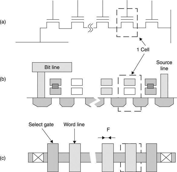
Uniform FN-tunnelling between the floating gate (FG) and channel was also introduced for the program/erase operation.2,3 As a result, source-to-drain voltage difference is kept at zero during programming. This enables cell size scaling, since there is no need for source-drain punch through during programming/erasing. Mass production was started in 1992 from 4 Mbit using 0.7 μm design rule. Cell size scaling has continued up to now. Since 2012, 128 Gbit has been in production using sub-20 nm design and 3 bit/cell technology. Trends in scaling of NAND Flash are shown in Fig. 2.2.
However, today a number of questions have been raised about the issues of further scaling of NAND Flash. The first is the instability of cell operation for program, erase and read.4–10 The second is related to reliability, mainly concerning data retention capability as a consequence of reduction of stored charges in FG, which are proportional to the capacitance CFG-CG between FG and the control gate (CG). The third is on process and integration issues, where the limitation comes from the lithography. Below 19 nm design, a water immersion stepper cannot practically be used, which leads to possible adoption of the complicated ‘twin side-wall’ process being required, unless Extra-Ultraviolet-Lithography (EUVL) becomes available to use for cost-sensitive volume production.
The first issues of cell operation margin reduction are discussed below:
1. Threshold voltage (Vt) distribution widening due to random telegraph noise (RTN): RTN occurs by electron trapping (detrapping) during program-verify read mode operation, and detrapping (trapping) at the normal read modes, which cause the threshold voltage distribution to become broader. This RTN effect becomes increasingly more serious with gate length and width (L,W) scaling.4,5 Moreover, it has been recently revealed that cell-to-cell spacing plays an important role in the RTN effect, due to source and drain doping concentration reduction.6
2. Vt distribution widening by FN-tunnelling statistics: FN-tunnelling current follows sub-Poisson statistics,7,8 which is translated to the distribution of the number of electrons transferring to/from the FG, thereby widening Vt distribution after programming. The dispersion of Vt variation at 1 program pulse [σ(ΔVt)] is roughly proportional to (1/CFG-CG)1/2, which implies that cell size scaling enhances the Vt distribution widening, almost proportionally to the inverse of the square root of cell’s W × L.
3. The short- and narrow-channel effects are more serious in the NAND Flash cell than in logic transistors, because of the scalability limit of tunnel-oxide thinning in order to avoid Stress Induced Leakage Current (SILK),9 especially in the case of 2 bit or 3 bit per cell operation.
4. Vt distribution widening due to the parasitic coupling of neighbouring cells, such as FG-to-FG or FG-to- channel coupling.10
As we move from 2D- to 3D-NAND Flash, we will still encounter the above issues, but somewhat differently:
1. The effect of RTN cannot be eliminated, even by using the 3D-NAND Flash cell, simply because memory cell size shrinkage will continue in order to reduce the cell size; the 3D-NAND cell uses intrinsic poly-Si for the channel, which will increase the RTN in gate-to-gate space; and the new RTN effect will occur at the grain boundaries in the thin film transistor (TFT) used for the memory cell.11
2. The 3D-NAND cell uses the SONOS (Si-Oxide-Nitride-Si) cell structure and the SONOS cell also uses FN-tunnelling or direct-tunnelling phenomena for program/erasing. This depends on the bottom oxide thickness, therefore Vt distribution widening by tunnelling current fluctuation would occur, similar to the case of 2D-NAND Flash.
3. 3D-NAND Flash has no narrow-channel effect because of the TFT structure, and can improve the short-channel effect by using a Gate-All-Around structure12 or twin-gate structure.13
4. By using the SONOS type cell in 3D-NAND, the neighbouring cell parasitic coupling effect can be improved by replacing thick FG by a combination of thinner oxide and SiN layer. However, this still remains an issue, even in 3D-NAND Flash, as long as the neighbouring cell space is small.14
2.3 3D-NAND Flash memory with vertical channels
2.3.1 BiCS cell
Structure, process and integration
There are two main kinds of cell structure that use vertical channels. One is called the BiCS (Bit Cost Scalable) cell, as proposed by Toshiba in 2007.12 The other is termed the TCAT cell (Terabit Cell Array Transistor), as proposed by Samsung in 2009.15 Both use vertical cylindrical poly-Si for the channel, but word lines (WLs) and two select gates (SGs) are horizontally stacked.
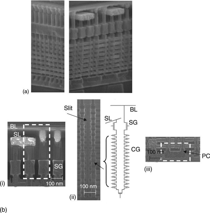
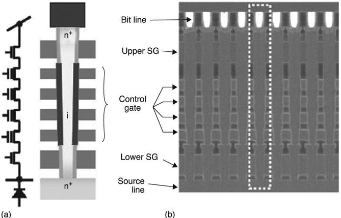
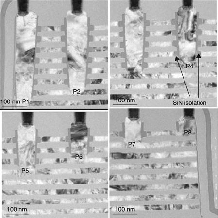
First, a review of BiCS cell structure is provided. A bird’s-eye sectional view of the BiCs cell16 is shown in Fig. 2.3. The cross-sectional view and equivalent circuit are shown in Fig. 2.4.17 A bird’s-eye scanning electron microscopy (SEM) picture of the BiCS cell is shown in Fig. 2.5(a).18 Figure 2.5(b) shows the cross-sectional SEM images for the 16-layered BiCS NAND strings fabricated by repeating the process steps for 8 layers.16 The channel is formed by a cylindrical poly-Si layer.

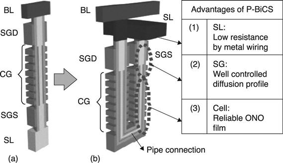
A junction-less undoped poly Si layer is used, because of the problems associated with atomic implant impurities. Thus, the space area of the poly NAND string must accumulate electrons by the fringing effect of the neighbouring gate during reading. The BiCS cell has a pipe-shaped channel, called the P-BiCS. Both edges of the channel are connected to a bit line (BL) and a source line (SL). Between the BL and SL, the P-BiCS cell has two selection transistors and plural memory cell transistors, with one pipe transistor at the bottom P-shaped channel. The diffusions of the selection transistors occur after the fabrication of the P-BiCS NAND strings. The gate insulator is formed by triple insulator layers, Si dioxide-Si nitride-Si dioxide (ONO). In the memory transistors, the Si nitride (SiN) layer acts as a charge storage layer to save the data, the so-called SONOS device. In conventional 2D-NAND Flash, a floating gate (FG) is used as the charge storage layer. The advantages and disadvantages of replacing FG with SiN are discussed in Section 2.4.
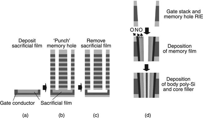
The basic process flow of P-BiCS is shown in Fig. 2.6.18 First, the insulator is deposited on the Si surface and a gate conductor is formed. Second, a sacrificial layer is deposited on the gate conductor (Fig. 2.6(a)). The gate conductor acts as the gate of the pipe transistor. Next, WL and select gates are stacked, with insulator layers sandwiched between them. Third, a vertical hole is made, with the subsequent removal of the sacrificial layer. Then, a P-shaped hole is made (Fig. 2.6(b,c)). Fourth, the ONO is deposited inside this P-shaped hole and undoped poly-Si is deposited there. Finally, a core filler insulator is inserted (Fig. 2.6(d)). In contrast to several of the 2D-SONOS-Flash memory devices, the Si dioxide layer must be formed by a chemical vapor deposition (CVD) process, not a thermal oxidation process. The thickness of the ONO is made up of 2.5 nm bottom tunnel oxide (TEOS), 11 nm SiN and 5 nm top oxide (TEOS).12 The quality of such a SONOS layer made using CVD bottom oxide is as yet unknown.
The previous BICS cell12 had a more simple structure (Fig. 2.7), with a straight poly-Si channel connecting top BL to bottom SL, and no P-shaped poly-Si channel. This was needed to be changed because of several problems relating to the straight TFT structure, such as poor reliability of memory cells, cut-off characteristics of the source side select gate and high resistance of the SL.18 For a straight poly-Si channel structure, the process flow is shown in Fig. 2.8.

First, an n+ layer is formed on the Si surface, and the plural insulator and WL stack are deposited. Next, holes are formed and the ONO layer is deposited. Then, the ONO layers at the bottom of the hole are etched and the poly-Si channel is deposited, to form a connection with the SL. In this process flow, the top oxide of the ONO layers is exposed to the etching conditions and quality of the bottom oxide could be degraded as a result. To avoid such degradation, pipe-shaped BiCS are proposed. The pipe gate also can reduce the resistance of the P-shaped TFT during reading. The quality improvements through using P-BiCS are summarized in Fig. 2.9.
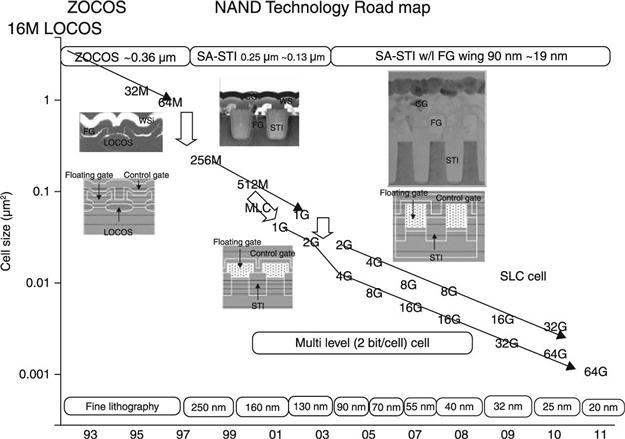
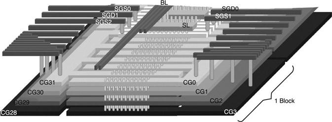
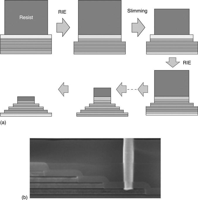
The complete P-BICS cell array is shown in Fig. 2.10.17 At the edge of the cell array, WLs (CG0 ~ 31) are picked up by contact with the top metal layers and these are connected to the row decoder’s transistor. In order to obtain the contact with the WL, a staircase pattern is used to shape the WL. This staircase structure can be achieved (Fig. 2.11(a)),12 and requires only one-time lithography patterning. A transmission electron microscopy (TEM) image of the contact to the stacked WL is shown in Fig. 2.11(b). Toshiba emphasizes that the number of mask steps can be kept the same, even though the number of stacks of WLs increases; this can help to minimize wafer cost.
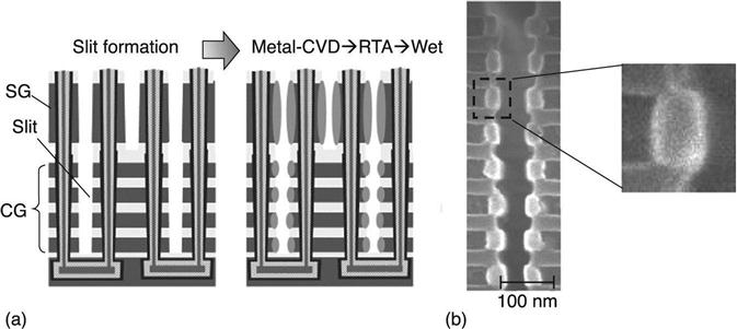
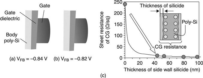
The WL (CGi) has a large capacitance between neighbouring WLs (CGi + 1, CGi − 1). During program and read, neighbouring WLs have a different bias setting and some RC delay occurs. The WL silicide process was therefore proposed to reduce the resistance (Fig. 2.12).18 A silicide process using poly-Si WL enables a sheet resistance of 11Ω/sq for a silicide thickness of approximately 42 nm (Fig. 2.13(c)). The flat band voltage (VFB) is stable, even though the layer that has undergone silicidation almost touches the gate oxide (Fig. 2.13(a,b)).
The estimated bit cost of BiCS Flash is shown in Fig. 2.14.19 There is a minimum hole size, which is limited by the thickness of ONO and radius of the body of poly-Si. Actual cell size is therefore mainly determined by the number of WL stacks. Generally, bit cost is inversely proportional to cell size and directly proportional to the process cost. For a simple stack of planar-type cells, the number of process steps is almost proportional to the number of stacks, so the process cost increases with increasing number of stacks. However, this is not the case when using the BiCS cell, which therefore implies a potential cost reduction when increasing the number of stacks. The number of WL stacks possible in a real production scenario is not yet known.

Program/erase/read operation
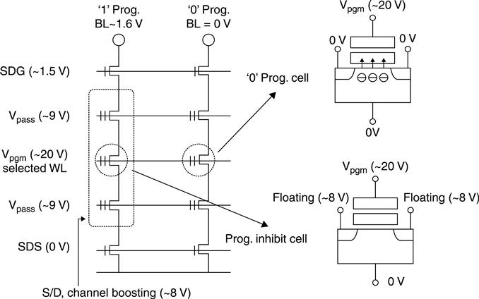
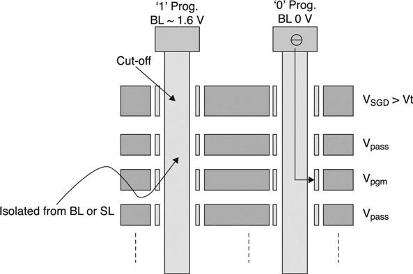
The program and read sequence is similar to conventional 2D-NAND Flash. During programming, a high voltage (Vprog) is applied to the selected WL with a medium voltage (Vpass) applied to the unselected WLs. In the case of 2D-NAND Flash, FN-tunnelling from channel to FG is used for programming, and from FG to channel for erasing. In the case of 3D-NAND Flash, FN-tunnelling or direct-tunnelling between the channel and SiN is used. Program disturb characteristics will be better than for conventional 2D-NAND Flash. In the case of 2D-NAND Flash, selection transistors from both sides cut off the NAND string from BL and SL at the ‘1’ programming string. Then self-boosting of the channel occurs, which can inhibit electron injection into the FG (Fig. 2.15). However, owing to the presence of the P-well, the electron flow inside the NAND string from the P-well cannot be easily cut off. By contrast, in 3D-NAND Flash, it is easier to cut off the electron flow to the program inhibit NAND string from the BL and SL, which in turn enables protection of the electron injection to SiN at the program inhibit cell (Fig. 2.16). This is one of the advantages of 3D-NAND Flash, owing to its thin film transistor structure.
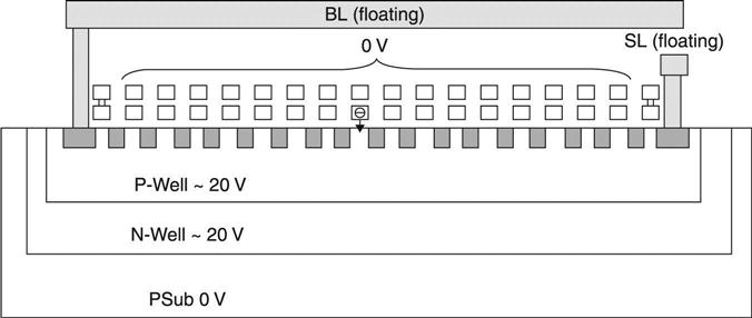
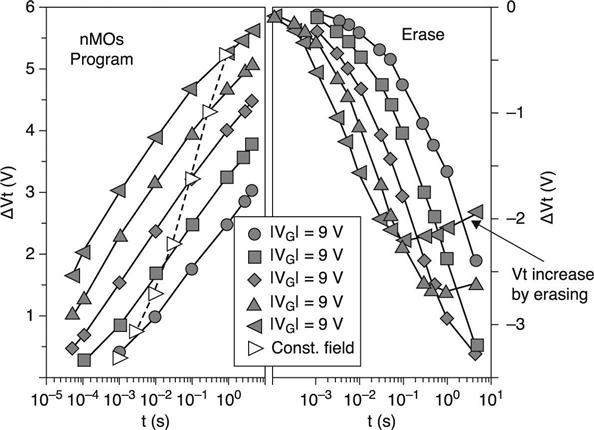
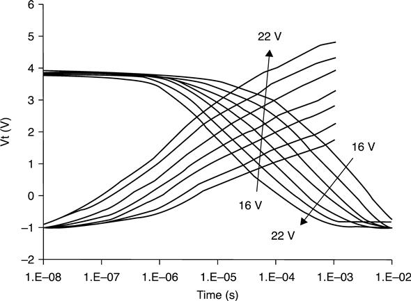
In the erase operation, high voltage is applied to the channel of NAND string with the WL grounded to extract electrons from the charge stored layer. In 2D-NAND Flash, it is easy to apply high voltage to the channel by applying high voltage to the P-well under the cell array (Fig. 2.17); however, in 3D-NAND, the P-well is absent. Thus, for the erase operation, the hole current into the NAND string, generated by GIDL near the lower select gates (USG and LSG), is used to raise the body potential (Fig. 2.18).21 High voltage is applied to BL and SL with lower select gate voltage to create band-to-band breakdown to generate the hole current. The program/erase (P/E) characteristics are shown in Fig. 2.19.18 For the BiCS cell, the Vt shift by erasing is more than 7 V, which is higher than for 2D-SONOS-Flash. This arises from the cell shape. The shape of the ONO is cylindrical and the electric field of the top oxide can be reduced as compared with the bottom oxide field. Thus, electron reverse-injection from the gate is unlikely to occur during electron emission from the SiN to poly-Si channel. Thus, Vt can be reduced when high erase voltage is applied to the BL and SL.

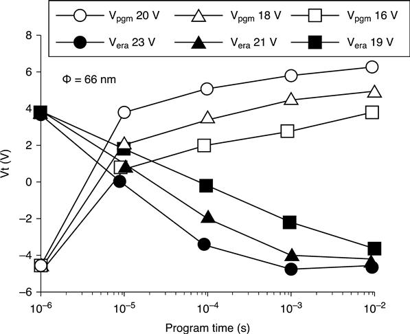
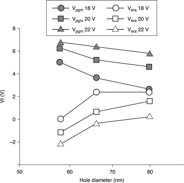
By contrast, the Vt of 2D-SONOS-Flash increases by applying high erase voltage (Fig. 2.20).20 This phenomenon can be explained by back-tunnelling of electrons from gate to SiN. The diameter dependence of the P/E window is shown in Fig. 2.21. The P/E window is enlarged by the smaller hole, because the electric field strength of the tunnel film is enhanced by the curvature effect.16 A comparison of program/erase characteristics between straight and pipe-shaped BiCS is shown n Fig. 2.22.16 A substantial improvement was observed at the P-BiCS, arising from the improvement in ONO quality.

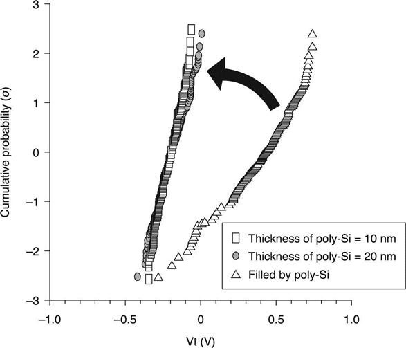
In reading, I-V characteristics strongly depend on the grain boundary in the poly-Si channel. The sub-threshold characteristics of poly-silicon Field Effect Transistors (FETs) are dependent on the location of the grain boundary and the trap density at the grain boundary, which in most cases cannot be controlled. In order to achieve better control, it has been proposed to use body silicon thinner than the depletion width (Wd).21 By using a thinner poly-Si body, the total number of traps can be reduced and the threshold voltage can be made less sensitive to trap density fluctuation; Fig. 2.23 provides an explanatory model. The structure of the ‘macaroni’ body vertical FET is shown in Fig. 2.24. Very thin poly-Si is deposited on the ONO layer. The hollow centre of the body is filled by dielectric film to make process integration easier. Figure 2.25 shows the drain current–control gate voltage (Id-Vg) characteristics of the macaroni body vertical FET; the I-V characteristics are improved.
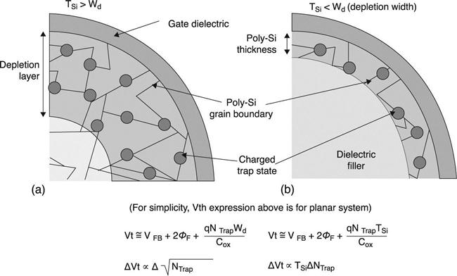
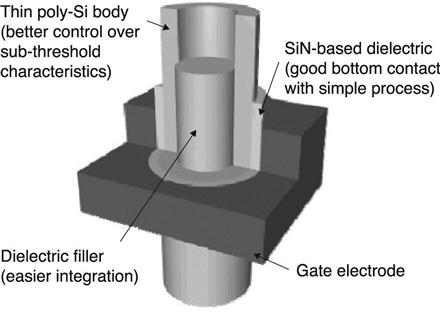

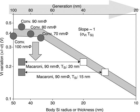
Figure 2.26 shows the simulated electric field across the vertical FET. The reduced body thickness enables better control of the channel potential by the gate electrode. A comparison between the Vt distribution of macaroni vertical FET and conventional, thick poly-Si FET is shown in Fig. 2.27.19 The Vt distribution width of the macaroni FET is narrower than for the conventional case. Measured Vth variations of several types of vertical FETs are plotted as a function of polysilicon body radius, or macaroni thickness (Fig. 2.28).21 Dispersion of the Vt variation can be reduced by making the body Si thinner. The macaroni body design offers better control to 30 nm generation; after that point, the diameter of the plug is small enough to suppress Vth variation. Details of Vt fluctuation by poly-Si grain are described in Section 2.4.
BiCS NAND Flash specification
Block size (erase cell unit) is number of WL in one string × number of cells in one WL × number of strings in one BL. The block size becomes very large as the number of WL stacks increases. Thus, the architecture of the NAND controller and file system using BiCS cell must be altered. The situation for the following TCAT cell is the same.
2.3.2 TCAT cell
The TCAT (Terabit Cell Array Transistor) cell was proposed by Samsung, using a vertical channel.15 A bird’s-eye view of the cell array and equivalent circuit are given in Fig. 2.29. Cross-sectional SEM pictures of the fabricated TCAT Flash cell array are shown in Fig. 2.30(a,b), where the NAND cell string has six cell transistors and two selection transistors (SSL, GSL) at the top and bottom.


The two selection transistors are formed simultaneously with the cell transistors. The TEM view of the cell in Fig. 2.30(c) shows a damascened metal gate with SONOS structure oriented vertically. The structural differences compared with the BiCS cell are:
• the line-type ‘W/L cut’ is etched through the whole stack between each row array of channel poly plugs;
• the line-type SL is formed by an implant through the ‘W/L cut’;
• metal gate lines are used to replace each row of poly plugs. The process sequence is briefly outlined in Fig. 2.31.
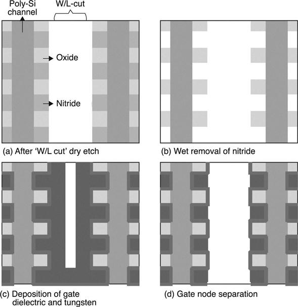
After ‘W/L cut’ dry etching and wet removal of the sacrificial nitride layer, the gate dielectric ONO layers and gate metal are deposited in the conventional order. This is not a ‘gate first’ process as for the BiCS cell. Separation of each gate node is followed by etching processes. The cell scaling trend is shown in Fig. 2.32, and is almost the same as for a BiCS cell. The SL resistance should be higher than for a BiCS cell by using an n+ Si layer as SL. Another important feature of TCAT NAND Flash is the bulk erase operation. As shown in the schematic representation of the structure in Fig. 2.33(a), the channel poly plug in the TCAT cell string is connected to the P-Si substrate at the bottom, not the n+ common source diffusion layer; this aspect differs from the straight BiCS cell. Therefore, a conventional bulk erase operation can be achieved, as displayed in the simulated profiles of Fig. 2.33(b). Other aspects of operation are the same as for BiCS.
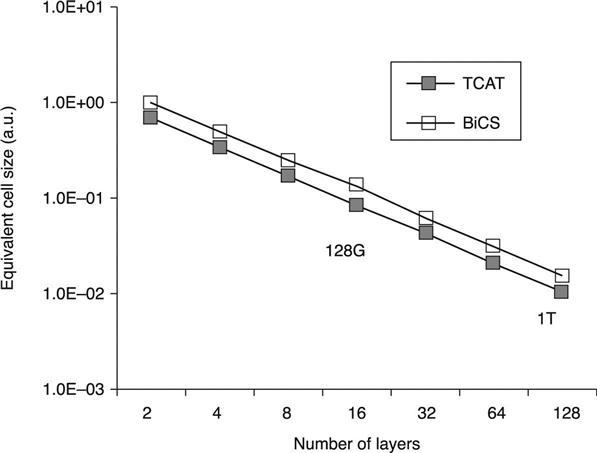
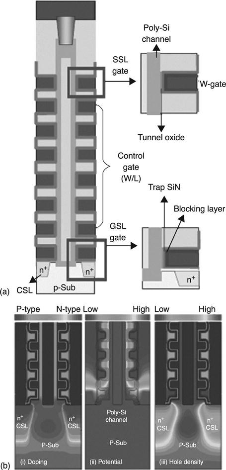
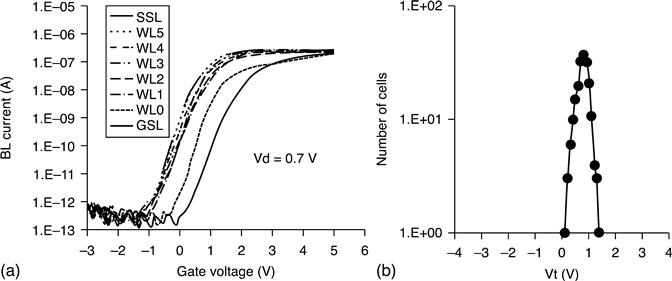
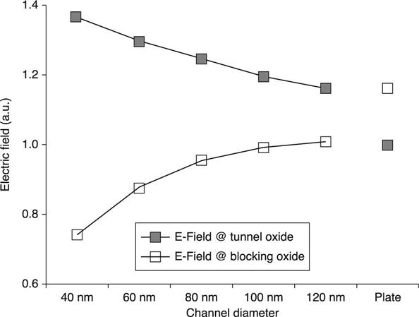
Figure 2.34(a and b) shows the Id-Vg characteristics of cell and selection transistors (GSL, SSL) in a single string and the Vth distribution of cell transistors of 32 strings, respectively. The sub-threshold slope is approximately 320 mV/dec and the on-off ratio is more than 106. Despite the poly-Si channel, the Id-Vg characteristics and Vth distribution are excellent due to the macaroni body effect, as found for the BiCS cell.21 Program and erase characteristics are shown in Fig. 2.35. Erase saturation occurs at approximately − 1 V, but depends on the channel cylindrical diameter. The data measure used in this figure is 120 nm. Checking of the productive channel diameter (~ 45 nm) is required for the erased Vt, because the electric field in the bottom tunnel oxide becomes stronger (Fig. 2.36), which is also similar to the BiCS cell.16
2.4 3D-NAND Flash memory with horizontal channels
2.4.1 VG cell
Structure, process and integration
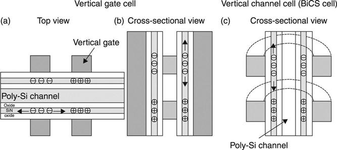
The horizontal channel cell differs from the vertical channel cell in that it has a vertical control gate (VG) and vertical select gate (VG). The vertical gate cell was proposed by Samsung in 2009.22 The BL and WL are formed before the deposition of several stacks of poly-Si channels. The vertical gate is formed after horizontal poly-Si channel patterning (Fig. 2.37). A brief process flow is shown in Fig. 2.38. The BL is fabricated first, then the WL is formed on top of it. Next, multi-active layers with p-type poly-Si are formed, and patterning is carried on the multi-active layers. Third, charge trap layers (ONO) are deposited over the patterned active layers. The VG is formed consecutively and connected to the WL. Finally, vertical plugs of DC and source-Vbb are connected to the BL and SL after contact ion implants. The N+ doped source and p-type active layer are electrically tied to the SL. The vertical WL needs to align with the horizontal WL. It is difficult to shrink the horizontal WL pitch to avoid the misalignment and process steps are complicated.
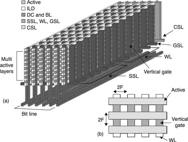
Key: Active, active area (source, drain, channel); ILD, inter layer dialectrics; DC, direct contact to bit line (BL); SSL, string select line; WL, word line; GSL, grounded select line; CSL, comon source line.
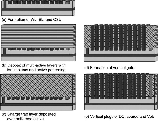
In 2011, Macronix also proposed a vertical gate 3D-NAND cell, which can eliminate the bottom BL and WL formation (Fig. 2.39).23 First, several stacks of insulator and undoped poly-Si are deposited. Then, patterning of the stacked insulator and poly-Si layers is carried out simultaneously. Next, the deposition of ONO dielectric and sequentially gate material fill the space between the horizontal stack of insulator and poly-Si. Patterning of the gate material is then carried out. Finally, the contact hole of the BL and SL is formed, connecting the stack of poly-Si layers and the deposits of SL and BL.
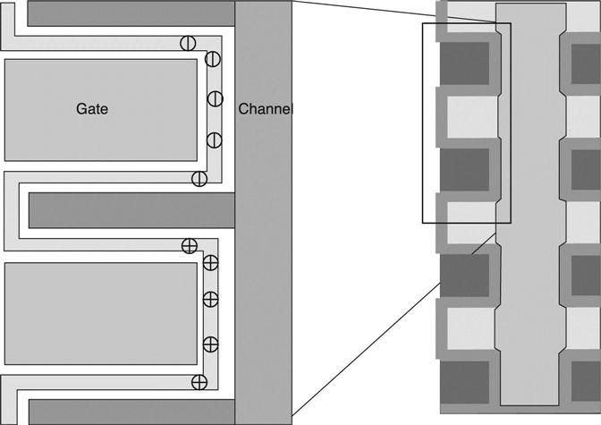
One of the difficulties with this vertical gate structure is how to select one horizontal poly-Si layer for program and read. One method is to create multiselect gates (SSL) between the BL and WL (Figs 2.37 and 2.40).22 In order to select one poly-Si layer, some selected transistors must be of the depletion type (normally ON) and others must be of the enhancement type. To distinguish between depletion and enhancement transistors, two kinds of channel doping and one heavy S/D implant are needed, which cannot be achieved by self-aligning to the SSL. Formation of plural select gates (SSL) requires some area penalty in each NAND string and the number of process steps for the channel implant increases as the number of stacks increases.

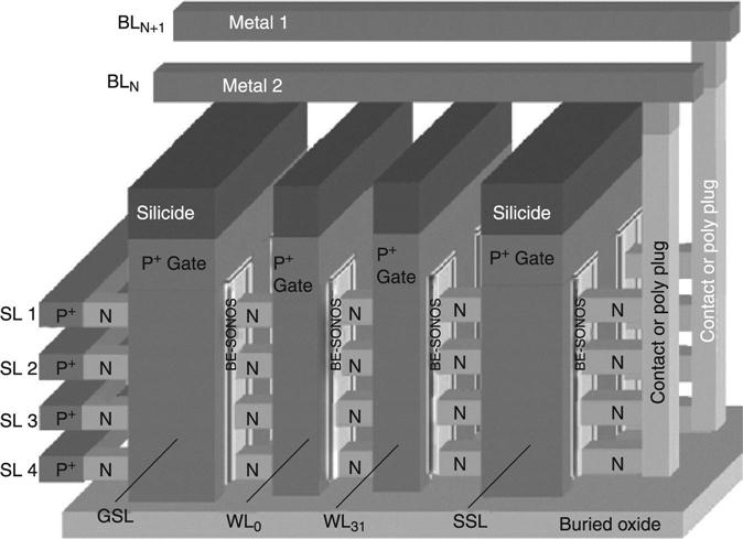
Another, more complex, method is shown in Fig.2.41.24 A schematic diagram of the twisted BL layout is provided in Figs 2.42 and 2.43, which will be termed here as the ‘VG twisted-BL cell’. When 8 horizontal poly-Si layers are stacked, a chunk of memory cells inside one horizontal plane is divided into 8 × 2 × M groups (page), where M is the number of WLs in one NAND string. First, memory cells in one horizontal plane are divided into two parts (even and odd poly-Si lines). Next, even (or odd) cells connected to one WL are divided into eight pages (the same as the number of poly-Si stacks). One set of even (or odd) consecutive eight NAND strings (each poly-Si channel is assigned a page, from 0 to 7) share one BL, and eight individual SSLs (selection transistors) select only one poly-Si channel among eight strings. Even cell groups have a contact to the BL at one edge of the NAND string, and odd cell groups also have a BL contact at the other edge of the NAND string. Each BL poly-plug has one connection to one BL-pad (red circle), and other poly plugs have no connection to this BL-pad (white circle) (Fig. 2.42(b)).
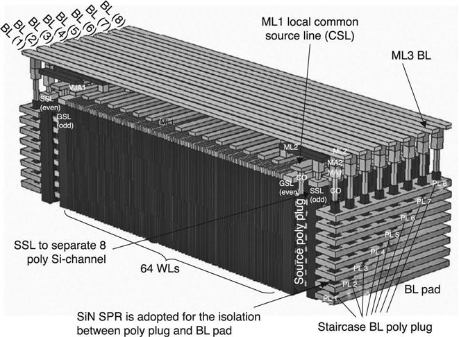
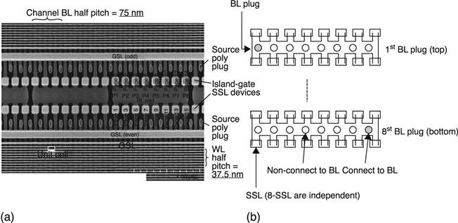
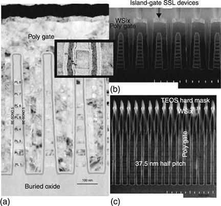
There are two BL-pads at both edges of one NAND string. Eight selection transistors (SSL) are independently connected to metal 2 lines (M2), and M2 lines are connected to metal lines (M1) parallel to the WL. M1 lines run from cell array area to row decoder, in the same way as the WL. There are also two SLs in one NAND string, at both edges of one NAND string. In total, for one pair of even and odd NAND strings, there are two sets of these (BL-pad, SSL, GSL, SL), where the GSL is a source-side selection transistor. Therefore, the NAND string length becomes larger. Figures 2.44(a, b and c) shows a SEM picture of the cross-section of the 8-layer cell array. Each poly-Si channel and oxide thickness is 30 nm. The inset in Fig. 2.44(a) shows the zoomed-in view, which reveals the double-gate TFT BE-SONOS charge-trapping memory cell. Figure 2.44(b) provides a cross-sectional view of the island-gate SSL device. The SSL has double-pitch of channel BL, and is fabricated together with the WL. Figure 2.44(c) shows a cross-sectional view of the 37.5 nm half-pitch WLs. At the top of the WL, there is a 60 nm-thick WSix to reduce the WL RC delay. Figure 2.45 shows the BL poly-plug connected to the BL contact. Before filling the poly-plug to the BL contact, a sidewall lateral recess is created to form the isolation between poly plugs and BL-pad.
Program/erase/read operation
The memory cell electrical characteristics should be basically similar to BiCS or TCAT cells. One structural difference is that the VG cell is sandwiched by twin control gates, not surrounded by a gate-all-around cell. Another difference is in the gate dielectric material. In case of the cell proposed by Macronix, use is made of BE-SONGS dielectrics, not ONO.25 The erasing method is the same as for a BiCS cell. By applying high voltage to the BL or SL with low select gate bias, GIDL hole current flows into the NAND string, which raises the channel body potential. The ONO shape of BiCS or TCAT is a cylinder. However, the equivalent VG-NAND shape is rectangular. Thus, the top oxide electric field is the same as the bottom oxide. BE-SONOS dielectric is necessary to suppress the reverse electron tunnelling from gate to SiN during erasing, which is different from BiCS or TCAT cells.
VG-NAND Flash specification
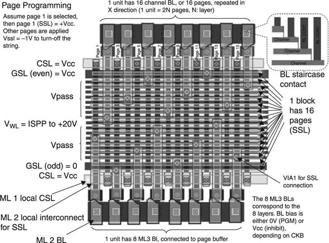
The spec of the ‘VG twisted-BL’ NAND Flash is described below. As explained in the previous terms of cell structure, a chunk of cells in one poly-Si plane have 2 × N pages when the number of the poly-Si stack is N. Cells in one page are programmed or read simultaneously. Thus, in the case of a 1 bit/cell, one WL has 2 × N × N pages, because Nth layer stacks have common WL. Then, the page number of a 2 bit/cell is 4 × N × N. If VG Flash has 8 layer stacks, one WL has 128 pages for 1 bit/cell. Figure 2.46 shows the programming characteristic, where BL24 is selected to program. Conventional 2D-NAND Flash has one or two pages in one WL, and a BiCS or TCAT cell will also have one or two pages, in the same way. Therefore, a very long time is needed for the programming and reading of one WL at a VG twisted-BL cell, compared with others. Accordingly, care should be taken to prohibit program disturb and read disturb, because of the longer stress time than for other cases.

2.5 Performance and electrical characteristics of different 3D-NAND Flash memory designs
2.5.1 Comparison of the performance of several 3D-NAND Flash memories
Table 2.1 shows a comparison between 2D- and 3D-NAND Flash memories.26 The sub-threshold swing decreases by approximately 30%, despite the carrier mobility degradation by approximately 85% due to the use of poly-Si channels. Moreover, in the 3D-NAND Flash, the parasitic cell-to-cell coupling can be reduced because of the gate-shielding structure, especially the vertical channel (VC) structure.
Table 2.1
Comparison of planar and 3D unit-cell structures. Cell size comparison is listed only including net cell area
| Dimension | 2D | 3D | ||
| Vertical channel | Vertical gate | |||
| Unit-cell |  |
 |
 | |
| Gate structure | Planar | Gate-All-Around | Dual-Gate | |
| Unit-cell size | 4F2 | 6F2 | 4F2 | |
| Barriers for physical scaling | Lithography | Film thickness | Lithography and film thickness | |
| 1 × nm node | Cell swing | 1 (ref.) | × ~ 0.75 | × ~ 0.7 |
| On-cell current | 1 (ref.) | × ~ 2.3 | × ~ 1.2 | |
| Coupling and direction | Strong WL + BL | Almost zero Vertical | Moderate BL + Vertical | |

Looking at the 3D array, as summarized in Table 2.2, the VC-NAND is less dependent on the lithography compared to the 2D-NAND, because the thicknesses of storage dielectrics and poly-Si channel determine the BL and WL pitches. The VG-NAND is still moderately dependent on lithography; however, because the WLs are patterned in the same way as the 2D-NAND, while BL pitch is determined by the total thickness of the channel, WL and storage layer. The cell size of VG-NAND will be 4F2 and of VC-NAND will be 6F2, considering the net cell area (Table 2.1). However, the VG-NAND will have a large cell overhead, including BL and SL contact and select gate area. VC-NAND, on the other hand, has almost no overhead area for the select gate and BL and SL contacts.
Table 2.2
Comparison of planar and 3D unit-cell structures, where overhead of (select gate and BL and SL contact) cell size in the NAND string is considered
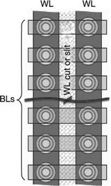
| Dimension | 2D | 3D | |
| Vertical channel | Vertical gate | ||
| Plane view | 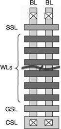 |
 |
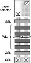 |
| Program/erase | FN | FN | FN |
| Major factors of program disturb | Channel coupling 1 (ref.) | NOP × ~ 0.2 | NOP and Vertical coupling × ~ 0.3 |
| Required stacks for 1 × nm node | – | 16 ~ 64 | 8 ~ 32 |
| Cell overhead | ~ 20 % | Almost zero | 35 ~ 70% |
| Lithography dependence | Strong | Weak | Moderate |
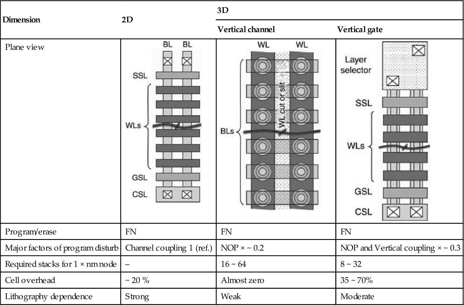
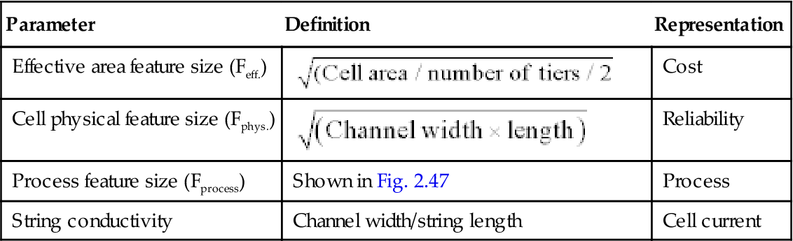
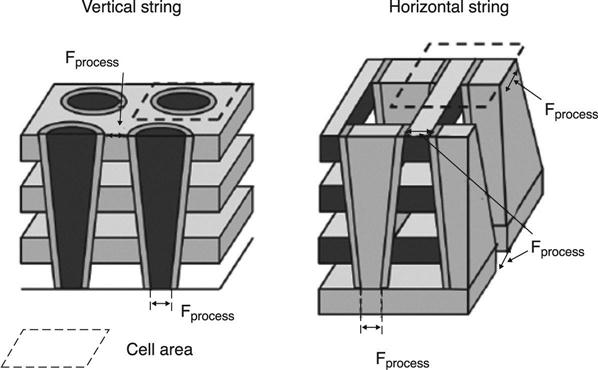
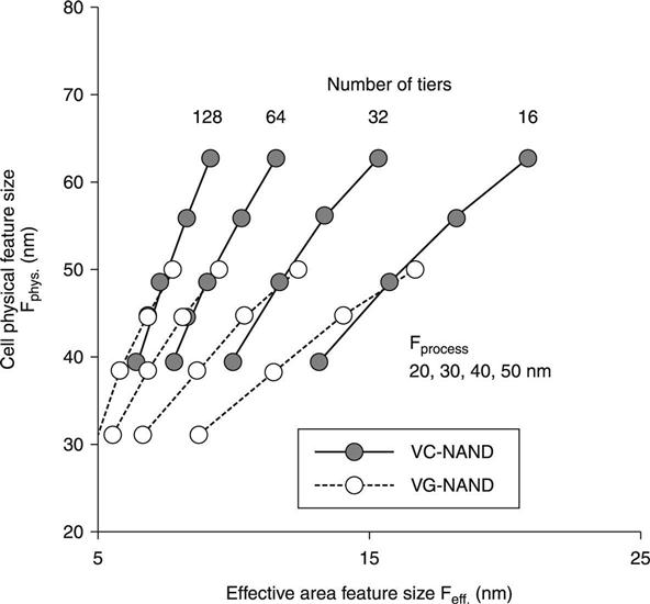
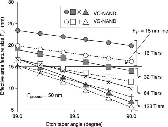
Table 2.3 summarizes key feature size definitions for 3D-NAND.27 The cell stack thickness (pillar to control gate distance) and tier thickness are kept constant in this analysis. Figure 2.47 defines the minimum feature size (Fprocess) of VC- and VG-NAND cells to compare the cell size in detail. Figure 2.48 shows the relationship between physical feature size and effective area feature size for 3D-NAND. The cell architecture and process parameters should be defined so that Fphys and Farea are optimally balanced. A near-vertical pillar profile is the key to achieving effective cell area scaling over 2D-NAND (Fig. 2.49). With a tapered pillar profile, the effective area scaling benefit from a tiered stack diminishes owing to a larger cell footprint at the top tier. Thus, knowing how the vertical pillar profile should be created is essential both for VC- and VG-NAND to scale the cell size. Here, the required number of tiers for VC-NAND was estimated; this has the same cell size as 2D-NAND with a 19 nm rule. The effective cell size of a 2D-NAND cell with 2 bit/cell will be 2.5F2 (= 2.5 × 192 nm2), which means Feff is 15 nm from the definition of Feff provided by Table 2.3. Assuming Fprocess at VC-NAND is 50 nm, 32 ~ 64 tiers are necessary to obtain the same cell size as the 19 nm rule 2D-NAND cell (Fig. 2.49). In this estimation, VC-NAND is assumed to be 1 bit/cell. In the case of VG-NAND, it is hard to estimate the real Fprocess or number of tiers to obtain the same cell size as 2D-NAND, because of the unknown factor of the cell overheads area of the BL, SL and select gates. When 3D-NAND can also use the 2 bit/cell, the number of tiers should become half.
Table 2.3
Feature size definitions for 3D NAND
| Parameter | Definition | Representation |
| Effective area feature size (Feff.) | Cost | |
| Cell physical feature size (Fphys.) | Reliability | |
| Process feature size (Fprocess) | Shown in Fig. 2.47 | Process |
| String conductivity | Channel width/string length | Cell current |
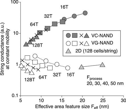
The channel conductance as a function of effective feature size is shown in Fig. 2.50. The larger channel width and shorter string length of the VC-NAND enhances string conductance by using the gate-all-around structure. Poly-Si channel mobility should be engineered to maintain this advantage. The poly-Si channel mobility requirement becomes more stringent as the number of tiers increases for the VC-NAND. The string conductance is more challenging for the VG-NAND, owing to its double-gate structure; however, the number of tiers can be increased without impacting the string conductance in the VG-NAND.
2.5.2 Electrical characteristics
Data retention
Generally the reliability of SONOS-Flash is worse than that of the FG type. One reason is the thinner bottom oxide in SONOS-Flash, which is less than about 4 nm. This is almost half the oxide thickness of 2D FG-NAND Flash. Thus, the leakage of current from the bottom oxide in 2D SONOS-Flash is larger than for FG-NAND Flash, and the data retention characteristics become worse than for FG Flash. The data retention characteristics of 3D-NAND should be the same as for 2D SONOS-Flash, which implies that data retention is worse than for 2D FG-NAND Flash.
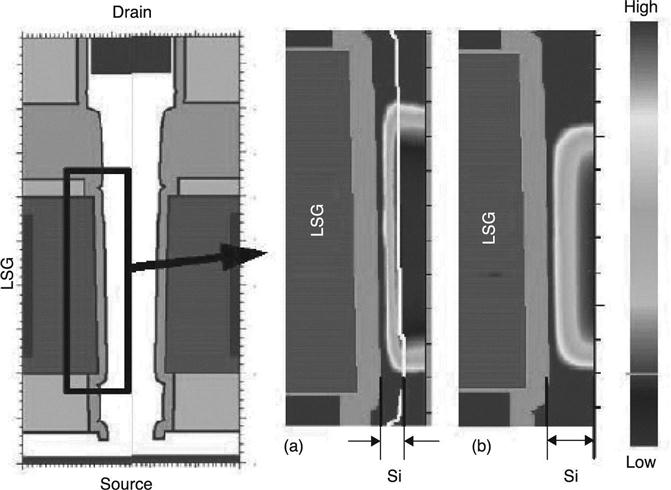
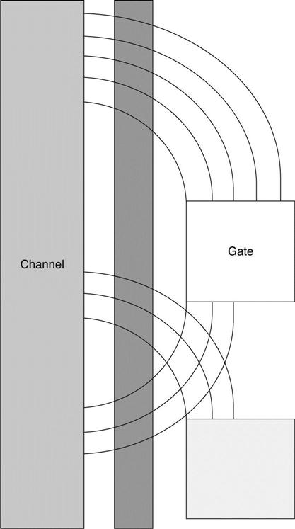
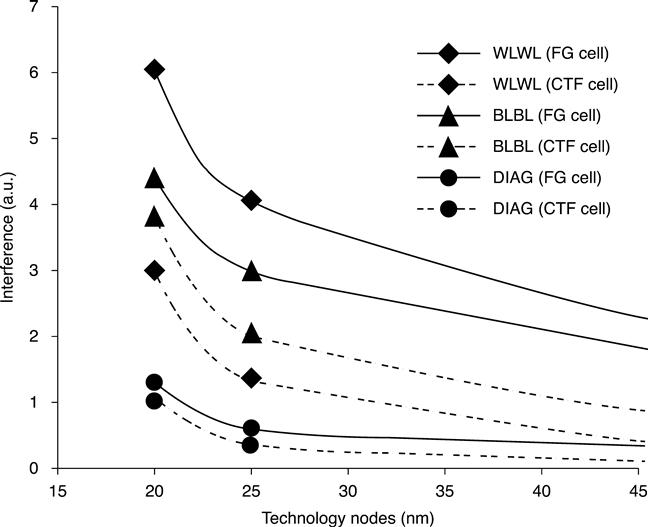
The next problem is electron diffusion inside the SiN layer. It is well known that during a high-temperature bake, there is a larger Vt drop when the SiN layer is not cut off from neighbouring cells (Fig. 2.51).28 The ΔVt depends on the neighbouring cell’s data, and a checkered pattern creates a lateral electric field inside the SiN, thereby helping electrons to diffuse into neighbouring cells. Thus, in order to obtain better retention characteristics, the SiN layer should be isolated from neighbouring cells. However, in the 3D-NAND Flash, this cannot be achieved, owing to the restriction of process/integration. In the case of VG-NAND Flash, there is another cell-to-cell interference occurring between two horizontal poly-Si layers (Fig 2.52(b)).

Among the three types of 3D-NAND Flash, the TCAT cell is superior at overcoming this issue (Fig. 2.53). Thus, to obtain better reliability, a longer WL-to-WL space and longer gate length are required. However, to obtain high cell current, the WL space needs to be smaller. Poly-Si FET is intrinsic and electron accumulation must be achieved by the fringing effect of the gate (Fig. 2.54). Thus, it is a trade-off between optimizing cell reliability and still obtaining a large cell current. These reliability issues have meant that the potential for 2 bit/cell operation has been unclear for 3D-NAND Flash, until now. However, by using FG-type NAND Flash, a 2 bit or 3 bit/cell will be possible. There are several proposals for FG-type 3D-NAND Flash.29,30 However, from the perspective of the constraint imposed by process integration, the FG type 3D-NAND Flash is more complex than the SONOS type 3D-NAND flash.
Vt distribution widening due to SiN to SiN coupling
It is well known that neighbouring FG-FG coupling causes undesired programmed Vt widening, when the gate space is narrower. Compared to FG-type NAND, the SiN layer is thinner. Thus, SiN-SiN coupling has a smaller effect than FG-type coupling, although the effect still cannot be neglected (Fig. 2.55).31
Erase Vt saturation phenomena
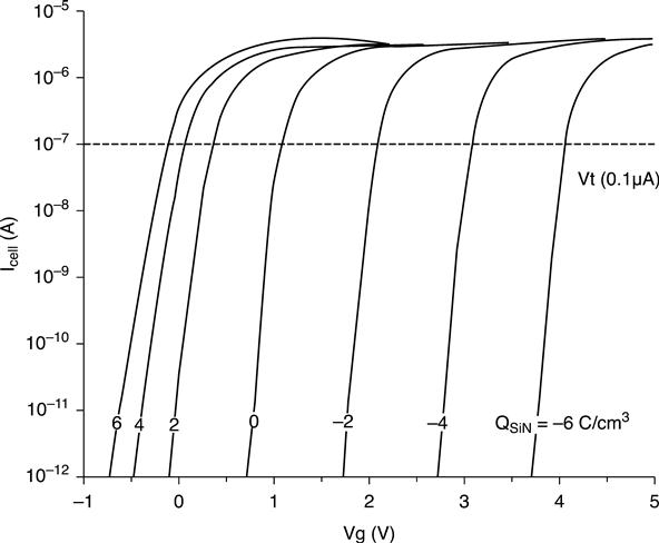
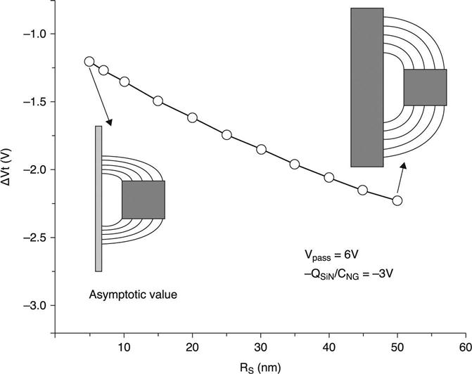
As poly-Si channel radius becomes smaller, the erase Vt saturation phenomenon occurs through using a junction-less NAND string.32 During reading, the gate voltage of the selected cell must be 0 V or negative when the selected cell is in the erased state. Thus, owing to the gate fringing effect, electrons in the WL-to-WL space regions are reduced, which results in a reduction of cell current. Figure 2.56 shows the cell I-V characteristics with various charges in the SiN layer. Vt is not proportional to QSiN, as QSiN becomes negative. This effect is becoming more serious as the poly-Si channel become thinner (Fig. 2.57). As explained in Section 2.2, erase Vt can be lowered as the poly-Si cylindrical radius is made smaller, because of the bottom oxide electric field enhancement during erasing. An optimized radius is necessary to achieve high erase efficiency.
Vt variation due to the poly-Si grain
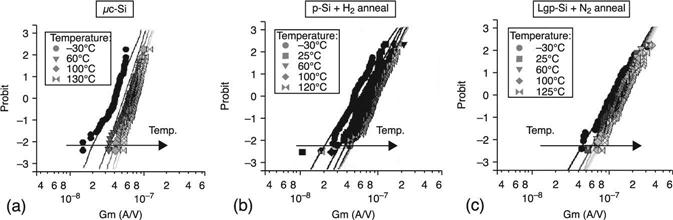
The poly-Si grain boundary induces a variation in I-V characteristics. There are many traps at the grain boundary, making a potential barrier ϕB. The potential barrier depends on grain size Lg and carrier density N (Fig. 2.58).33 Grain boundary conductance is proportional to exp(− βϕB), which has strong dependence on temperature, and increases Vt while reducing Gm. The grain size dependence of Id-Vg characteristics has been studied with different poly-Si processes.34 Three undoped poly-Si process options are compared according to their average grain size:
1. low-pressure CVD (LPCVD) poly-Si in a hydrogen atmosphere leading to small grain size, referred to herein as microcrystalline poly-Si; uc-Si;
2. conventional LPCVD poly-Si leading to intermediate grain size; p-Si; and
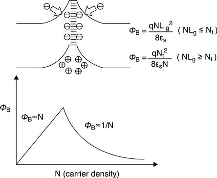
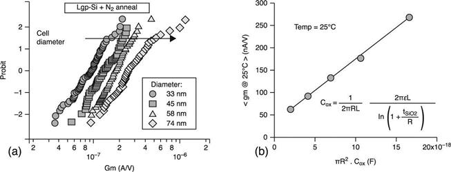
Figure 2.59 shows the Gm values for different channel materials and temperatures. High temperatures result in a larger grain size, and larger grain poly-Si also results in larger Gm. Cylindrical cell diameter dependence on Gm at RT is shown in Fig. 2.60(a). A smaller diameter results in smaller Gm. The average value of Gm can be described as proportional to cylindrical size (πR2) multiplied by gate oxide capacitance (Cox) (Fig. 2.60(b)). Thus, in order to obtain a high cell current, the cell diameter cannot be too small.
For the case of a double gate VG-NAND cell, TCAD simulation results have been obtained with and without a grain boundary at the cell channel region, where grain size is estimated to be 20~50 nm.35 The simulation results in Fig. 2.61(b) indicate that the case with a grain boundary between the gate-to-gate space undergoes less degradation than in the fresh state (no Dit), whereas the case with a grain boundary under the channel has significant sub-threshold degradation and higher Vt. In Fig. 2.61(c), the many Id-Vg curves of the random grain boundary locations are compared with each other. Interestingly, the currents merge at a very low current level (< 1 fA, beyond the typical measurement resolution). Theoretically, the merged point corresponds to the mid-gap voltage, where the interface trap becomes charge neutral and unable to affect the sub-threshold current.

2.6 Conclusion
In this chapter, several electrical characteristics of 3D-NAND cell are overviewed, which is different from conventional 2D-NAND cell. These are the drawback of 3D-NAND. However, one advantage of 3D-NAND cell is its ability to use relatively larger cell size. In the case of VC-NAND (BiCS and TCAT-cell), gate length can be longer than 2D-NAND cell. In the case of VG-NAND, longer channel width can be used. The cell reliability can be improved by this advantage. From now on, the NAND Flash maker will make a lot of effort to improve 3D-NAND cell reliability as well as to make smaller effective cell size.