Ferroelectric random access memory (FRAM) devices
T. Eshita and T. Tamura, Fujitsu Semiconductor Ltd, Japan
Y. Arimoto, Fujitsu Laboratories Ltd, Japan
Abstract:
We review the history of, and recent advances in, ferroelectric memory, including ferroelectric random access memory (FRAM or FeRAM). FRAM is the first among advanced non-volatile memories, such as magnetoresistive random-access memory (MRAM), phase-change random access memory (PRAM) and resistive random access memory (ReRAM), to be commercialized. Highly reliable FRAM with a memory density of a few Mb is currently available. Since FRAM has excellent electric properties, such as a high speed read/write (< 50 ns), high switching endurance (![]() 1013) and low power consumption, it has been applied to radio frequency identification (RFID) tags, advanced smartcards and so on. We also describe newly developed materials, fabrication processes and circuit technology, which are expected to overcome the scalability problem of FRAM.
1013) and low power consumption, it has been applied to radio frequency identification (RFID) tags, advanced smartcards and so on. We also describe newly developed materials, fabrication processes and circuit technology, which are expected to overcome the scalability problem of FRAM.
Key words
FRAM; FeRAM; ferroelectric; PZT
14.1 Introduction
Ferroelectric memory, including ferroelectric random access memory (FRAM or FeRAM), is non-volatile memory which stores information as a polarization state of the ferroelectric material. Ferroelectric material has bistable polarization states, which are retained even in the absence of an external electric field, and can be easily switched between states by applying such a field (generally < 100 kV/cm). Since FRAM has excellent electric properties, such as a high speed read/write (< 50 ns), high switching endurance (![]() 1013) and low power consumption in comparison with conventional FLASH memory, it has been applied to radio frequency identification (RFID) tags, advanced smartcards and authentication devices.
1013) and low power consumption in comparison with conventional FLASH memory, it has been applied to radio frequency identification (RFID) tags, advanced smartcards and authentication devices.
In 1951, Pulvari described a possible means of information storage using a ferroelectric material (barium titanate).1 It is interesting that he proposed to operate this ferroelectric memory a few degree below the Curie temperature (Tc) to achieve low power consumption and high read/write speed. In 1955, four years from this proposal, a semiconductor- based ferroelectric memory was proposed by Ross.2 In the late 1980s, some start-up companies in the US began the development of practical Si-based capacitor-type FRAMs3,4 and many electronics companies around the world started competing in the development of FRAM, aiming to realize ‘a dream memory’ capable of high speed read/write and non-volatile. By the late 1990s, several US and Japanese companies, 5–7 were successfully mass-producing FRAM with memory densities of 16 to 256 Kb. Recently, FRAMs of up to 8 Mb, and many kinds of embedded FRAMs, have been commercialized. This chapter aims to describe the history and recent advances in FRAM.
14.2 Basic properties of ferroelectric capacitors
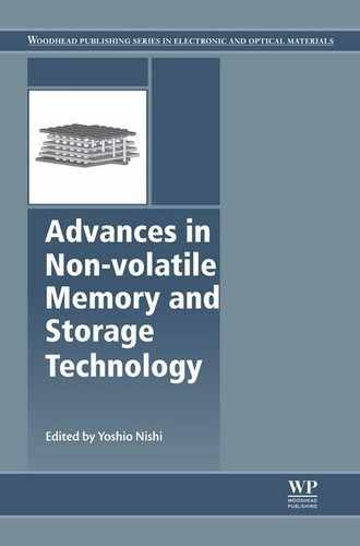
In this section, basic properties of ferroelectric capacitors are briefly described to help understand the following sections. Ferroelectric material has a spontaneous polarization, which can be reversed by applying an external electric field. When such an electric field is applied to a ferroelectric capacitor, a polarization-electric field (P-E) hysteresis curve is obtained (Fig. 14.1). A coercive field (Ec) is defined as the strength of the electric field at which the macroscopic polarization of the ferroelectric capacitor disappears. Polarization remaining in the absence of an electric filed is called the remnant polarization (± Pr), where ‘±’ corresponds to the direction of polarization. In a FRAM, stored data are read by measuring the voltage derived by polarization reversal or non-reversal current.
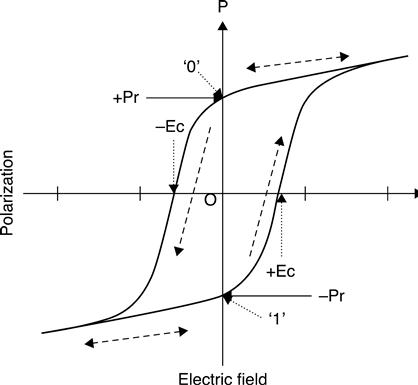
In a ferroelectric crystal, spontaneous polarization is derived from relative displacement of anions and cations. For example, in lead zirconate titanate (PbZrxTi1-xO3, 0 < x < 1; PZT) (Fig. 14.2), the Ti4+ or Zr4+ ions occupy one of two possible stable positions. Since neither of these two positions are charge centred in a unit cell, an electric dipole is spontaneously generated. The relationship between energy potential and ion displacement is shown schematically in Fig. 14.3. The Ti4+ or Zr4+ ions occupy one of the two stable positions and can be moved between the positions by applying an external electric field. As temperature increases, a bistable state merges into a single stable state. This critical temperature is called the Curie temperature (Tc). While the crystal structure of PZT, whose c-axis is slightly longer than the a- and b-axes, is tetragonal below Tc, it becomes cubic above Tc, where the length of the a-, b- and c-axes are all equal (phase change). More precisely, the energy potential in the case of the second-order phase change, where free energy changes continuously with temperature, is shown in Fig. 14.3. There also exists a first-order phase transition, where free energy changes discontinuously with temperature.8 The temperature dependence of polarization is described as
[14.1]

where P(0) and T are polarization at 0 K and temperature, respectively. Viewed microscopically – a local region of hundreds of nm – the ions occupy the same side of the double-well (Fig. 14.3). This region is called a domain, and is generally smaller than a ferroelectric polycrystalline grain.
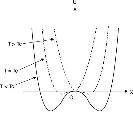
Polarization switching speed is one of the issues of most concern for FRAM engineers. Theoretical investigation has been carried out by Ishibashi.9 As shown in Fig. 14.4, switching time generally consists mostly of a nucleation time (the time needed for the initiation of the polarization reversal point – only nucleation domains larger than a critical size remain, with smaller domains disappearing), a propagation time and a domain growth time.8 In experimental measurements of a PZT capacitor, switching time is found to be in a range between a few ns and a few tens of ns.10,11
14.3 Ferroelectric materials used for FRAM devices
Discovery of P-E hysteresis of ‘Rochelle salt’, the first material to be reported exhibiting ferroelectricity, goes back to the end of the 19th century.12,13 Debye introduced a hypothesis of ‘permanent electric dipole’ to explain the P-E hysteresis, and Schrödinger proposed the concept of ferroelectricity as an analogy to ferromagnetism in the early 1910s. Valasek successfully explained his experimental results of P-E hysteresis using the concept of ferroelectricity in 1920, in which he proved the existence of the ‘Curie Point’ in ferroelectrics (Rochelle, salt).14
During World War II, new piezoelectric materials were investigated in several experiments for the improvement of the sensitivity of submarine detection sonar. In the early 1940s, barium titanate (BaTiO3), the first man-made perovskite ferroelectric material, was synthesized independently in the United States, the USSR and Japan. In the late 1940s, Devonshire developed his phenomenological model of ferroelectrics on the basis of Helmholtz free energy. In the 1990s, the application of BaTiO3-SrTiO3 solid solution to increase the capacitance of a DRAM capacitor was attempted.15
Lead zirconate (PbZrO3 or PZO), lead titanate (PbTiO3 or PTO) and their solid solution system (PbZrx Ti1-xO3 or PZT), belonging to the perovskite family, are the most important ferroelectric materials being used by most commercialized FRAMs. Waku and Hori found the phase transition of PTO in the summer of 1949, which was referenced by Shirane.17,18 According to the PZT phase diagram derived by Jaffe et al., 19 while Ti-rich PbZrxTi1-xO3 (x > 0.52) has a tetragonal crystal system near room temperature, Zr-rich PZT has a rhombohedral one. The Pr and c/a-axis ratio increases with increasing the Ti/Zr composition ratio. In the phase diagram, the tetragonal-rhombohedral boundary (composition ratio is nearly x = 0.52) is called the morphotropic phase boundary (MPB). Impuritydoped PZT is usually used for FRAM capacitors, as it has been reported that doping with La20,21 or Nb22,23 is effective for improving the leakage current, fatigue and imprint (Section 14.5.2) of PZT capacitors. Fox et al. reported that La and alkaline earth metals doping can reduce the saturation voltage of PZT, which lowers the operation voltage of the FRAM.24 In the late 1980s and early 1990s, many attempts were made to apply PZT to DRAM capacitors to increase their capacitance, and so increase memory density.25,26
Other important ferroelectric materials are bi-layered perovskite materials (also referred to as ‘Aurivillius phase’,27 whose crystal structure consists of a (Bi2O2)2– sub-layer and a (Ax-1BxO3x+1)2+ perovskite sub-layer, where A and B stand for cations.29,30 In 1974, Bi4Ti3O12 (BIT) was applied to Si-based FRAM by Wu.31 In 1995, Araujo et al. found that SrBi2Ta2O9 (SBT), SrBi2NbTaO9 (SBTN) and SrBi4Ta4O15. are immune to ‘fatigue’ (Section 14.5.2),32 and FRAM using SBT or SBTN has been developed by many companies.33,34 Both SBT and SBTN have smaller coercive fields and saturation polarizations than PZT.
Since the beginning of the 21st century, BiFeO3 (BFO) has attracted much research because of its larger 2Pr (~ 100 μC/cm2) and low deposition temperature.35 However, the BFO large coercive field (~ 550 kV/cm – the Ec of PZT is ~ 65 kV/cm) and large leakage current have hindered its application to FRAM. Doping with impurities such as Mn and Ti has proved to be effective in reducing both Ec and leakage current. Hu et al.36 and Kawae et al.37 achieved low leakage current and low Ec (~ 300 kV/cm) while maintaining high Pr. BFO is an exotic ‘multiferroic’ material exhibiting different electric and magnetic states simultaneously, and it is expected to provide the opportunity to encode information in both electric polarization and magnetization, to obtain four logic states. Four-state memory has already been demonstrated using similar multiferroic material, La0.1Bi0.9MnO3 (LBMO) by Gajek et al.38
Recently Müller et al. found that impurity (yttrium or silicon) doped HfO239,40 and ZrO2-HfO2 compound (ZHO)41 have stable ferroelectric phases at room temperature. They reported a Pr of 16 μC/cm2 for Y-doped HfO2 and 24 μC/cm2 for ZrO2-HfO2. However, the Ec of these materials is about 1 MV/cm, which is much larger than that of PZT (~ 65 kV/cm). They also found that, when heating their specimen under mechanical confinement, an orthorhombic ferroelectric phase of Si-doped HfO2 reversibly transforms into a phase displaying anti-ferroelectric behaviour.
The application of ferroelectric organic polymers to non-volatile memory is attractive because of the low cost manufacturing and the realization of transparent, flexible and wearable FRAMs. Since the strong piezoelectricity of polyvinylidene difl uoride (PVDF) was discovered in 196942 and its erroelectricity was suggested in 1971,43 many investigations of its application to memory have been reported. Schroeder et al. reported ‘an All-Organic Ferroelectric-Like Memory Transistor’ using poly-(m-xylylenediamine-alt-adipic acid)-(MXD6), which revealed an ON/OFF-drain- current ratio of about 3 × 104.44 ‘Ferroelectric-like’ means that the P-E hysteresis exhibits the same shape as typical ferroelectric materials without the typical thermodynamic phase. Fujisaki et al. reported that their fabricated P (VDF–TrFE) ferroelectric capacitor has a Pr of 11.9 μC/cm2 and an Ec of 333 kV/cm (fi lm thickness is 60 nm).45 Sekitani et al. proposed the concept of ‘Communication sheets using printed organic non- volatile memories’.46 They showed that the ‘1–0’ ratio of their fabricated organic FRAM exceeded 103 after 104 cycles in air.
14.4 FRAM fabrication processes
Commercialized Si-base FRAM has been fabricated by combining ferroelectric capacitor and conventional CMOS fabrication processes. Since the temperature(s) of ferroelectric deposition and/or its crystallization are usually higher than those of the metallization process, a ferroelectric capacitor fabrication process is usually inserted between a transistor fabrication process (front end of line: FEOL) and a metallization process (back end of line: BEOL). In comparison with the Flash memory process, where an additional high voltage transistor fabrication process is needed, the FRAM process is much simpler, because FRAM memory cells can use logic transistors ‘as is’. This is especially advantageous when fabricating FRAM embedded logic devices. Noble metals, such as Pt, Ir and IrO2, are usually employed for capacitor electrodes for the same reason (and also because they have high work functions). In addition, high temperature proof perovskite-base electrodes have also been proposed.47
There are two different types of ferroelectric capacitor structure. One is a planar capacitor structure7,22 and the other is a stacked capacitor structure48–51 (Figs 14.5 (a and b), respectively). In the fabrication process of the planar capacitor, a ferroelectric capacitor is placed above field insulator layers (generally referred to as shallow trench isolation (STI) or local oxidation of silicon (LOCOS)) after planarization of a dielectric layer over the metal oxide semiconductor field-effect transistor (MOSFET). Electrical contacts between the capacitor electrodes and the MOSFETs are made following dielectric interlayer deposition over the capacitor. This process is relatively easier than the stacked capacitor process, though the unit memory cell area is larger.
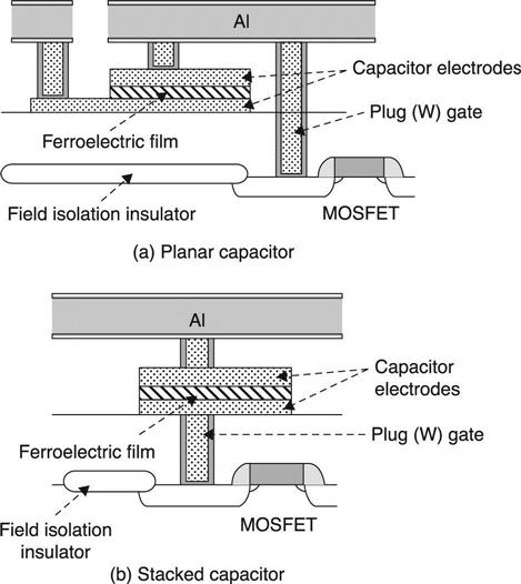
In the stacked capacitor process, a bottom electrode of ferroelectric capacitor is disposed directly onto the contact metal (usually W) connecting to a MOSFET, a very fine bottom electrode structure, and/or materials have to be employed to avoid the oxidation of the contact metal during the high temperature ferroelectric process. Oxygen barrier metal such as TiN, Ir, IrO2 and/or their stacks are commonly used for a bottom electrode. The stacked capacitor has the advantage of small memory cell area, even though the fabrication process and materials required are slightly more complicated than those of a conventional planar CMOS process.
For ferroelectric film formation, physical vapour deposition (PVD) mainly using sputter deposition,7 metal organic chemical vapour deposition (MOCVD)52,53 or chemical solution deposition (CSV) mainly using spin coating,5 have been employed. Electrodes are usually deposited by PVD. Although the deposition costs of PVD and CSD are relatively lower than MOCVD due to low source cost and high throughput, the MOCVD method has the advantage of precise source material controllability.
In the ferroelectric capacitor etching process, conventional reactive ion etching (RIE) cannot be employed since noble metal, which are used both for top and bottom electrodes, are not reactive and the vapour pressures of by-products from ferroelectric materials are extremely low. Therefore, physically-assisted RIE is employed by using argon-mixed etching gases.
14.5 Ferroelectric memory cell structure of capacitor-type FRAM devices
14.5.1 Capacitor-type FRAM with a DRAM-like memory cell
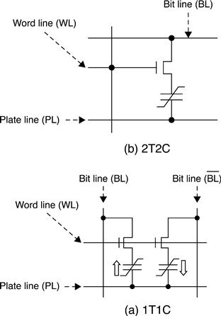
This type of FRAM comprises a ferroelectric capacitor and a memory circuit, which is similar to a DRAM circuit.3,4 It should be noted that FRAM has a plate line that is applied by the read/write operation voltage, while DRAM usually has a cell plate structure whose voltage is fixed at 1/2 supplied voltage (Vdd). There are two types of memory circuit; one is one transistor and one capacitor (1T1C) and the other is two transistors and two capacitors (2T2C) (Figs 14.6 (a and b), respectively). While 1T1C FRAM is suitable for large memory density due to its small memory area, 2T2C FRAM is highly reliable due to two complementary memory units, even though the memory area is larger. High density (![]() 1 Mb) FRAMs were proposed by several electronics companies in the late 1990s and early 21st century, using 1T1C stacked capacitors.42–45 Currently up to 8 Mb FRAMs have been commercialized.
1 Mb) FRAMs were proposed by several electronics companies in the late 1990s and early 21st century, using 1T1C stacked capacitors.42–45 Currently up to 8 Mb FRAMs have been commercialized.
14.5.2 Write/read operation in the capacitor-type FRAM with a DRAM-like memory cell
In this section, the basic write/read operation of a capacitor-type FRAM with a DRAM-like memory cell is briefly explained (Fig. 14.7). In a write operation, first the bit line is set to a high or low level. After turning on the selection transistor, a voltage pulse is applied to the plate line. Data ‘0’ is written on the capacitor while the plate line is at the high level (Fig. 14.7(a)); data ‘1’ is written when the plate line turns back to the low level (Fig. 14.7(b)). This operation allows bi-directional application of the full supply voltage to the capacitor, switching the polarization sufficiently. In a read operation, the bit line is firstly pre-charged at 0 V and then set to floating. After turning on the selection transistor and driving the plate line to the high level, charge flows to the bit line from the cell capacitor, resulting in a bit-line voltage increase.

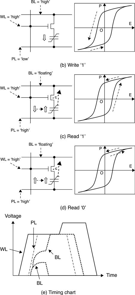
While polarization reversal charges flow to the bit line when reading ‘1’ (Fig. 14.7(c)), linear charges flow to the bit line when reading ‘0’ (Fig. 7(d)). The increase in the bit line voltage from reading ‘1’ is usually larger than that from reading ‘0’, because the polarization reversal charge is larger than the linear charge. Note that the above-mentioned read operation for FRAM is sometimes called ‘a destructive read’, because it needs polarization reversal to read data. With an amplifier of 2T2C-type, FRAM determines ‘0’ or ‘1’ by comparing the states of the paired capacitors, whereas with an amplifier of 1T1C type, FRAM determines the state by comparing the bit line voltage and the reference voltage. The polarization reversal charge depends on condition of the ferroelectric capacitor, which could become small if the capacitor is degraded by depolarization, imprint or fatigue as mentioned below. Thus, the sensing margin of 1T1C FRAM strongly depends on the reference voltage.
Therefore, 2T2C FRAM is generally more robust than 1T1C FRAM (although the 2T2C cell area is larger). This reading operation is called a ‘High-Z’ sensing scheme, which means a high impedance. In this scheme, externally supplied voltage (Vdd) is not fully applied to each cell capacitor, because the supplied voltage is reduced by Cb/(Cb + Cs) due to the floating bit line, where Cs and Cb are the capacitance of capacitors and bit line, respectively. To improve the sensing margin in the high density FRAM, a bit line ground sensing (BGS) technique has been proposed by Kawashima et al.54 In their sensing scheme, since the p-MOS charge transfer maintains the bit line level near to ground when the plate line is high, almost the entire external voltage can apply to each cell capacitor, which results in a drastic increase in the sensing margin.
Precise prediction of the polarization switching behaviour is essential in the design of the FRAM. However, no such simulation models exist because of the complex hysteretic behaviour. Polarization switching speed depends significantly on applied voltage, and hence the hysteresis loop depends on the voltage variation rate. The coercive voltage (the voltage corresponding to the coercive field) varies, depending on the condition as well, although it is treated as a fixed value in commonly proposed models. A circuit simulation model has been proposed, which reproduces the behaviour of polarization switching at any voltage conditions. The parallel element model consists of a group of capacitor elements, each of which has a (fixed) coercive voltage and remnant polarization. By giving each element voltage-dependent switching time, the model reproduces the hysteresis behaviour of the capacitor over a broad voltage range. The model also expresses the degraded states of the ferroelectric capacitor (imprint or fatigue), which becomes a valuable tool in the design of FRAM circuits immune to ferroelectric degradation.55
14.5.3 Other capacitor-type FRAM
Dimmer and Eaton proposed ‘non-volatile [shadow random access memory] SRAM’ consisting of six transistors and two ferroelectric capacitors (6T2C),6 which works as normal SRAM (non-destructive read) in the existence of an external power supply, but stores the information on ferroelectric capacitors in the absence of an external power supply. Therefore, this type of FRAM has the capability of both high speed read/write (almost equal to conventional SRAM) and non-volatility. Masui et al. proposed a non-volatile SRAM with a 6T4C structure to improve the ‘recall operation’ of 4T2C FRAM.57 They have proposed that their 6T4C non-volatile SRAM, with an access speed of 4 ns, could be applied to a high performance dynamically programmable gate array (DPGA). A non-volatile logic, similar to non-volatile SRAM, in which storage elements are distributed over the logic-circuit plane, has also been proposed to lower the power consumption. Standby currents in distributed storage elements can be cut off using ferroelectric-based non-volatile storage elements.58
To reduce memory cell area, a ‘chain FRAM’ was proposed, which comprises parallel connection of one transistor and one ferroelectric capacitor. One memory cell block consists of multiple memory cells connected in series with a block-selecting transistor. It has been reported that a unit cell area of 4F2 could be realized by using chain FRAM confi guration.59
14.5.4 FET-type FRAM (FeFET)
In a field effect transistor (FET)-type or one transistor-type FRAM, a ferroelectric insulator layer is applied to the gate of the FET (Fig. 14.8). Information is stored in the gate ferroelectric layer and read out as transistor drain current, since the polarization direction of the ferroelectric layer determines the transistor threshold voltage. It is advantageous that this type of FRAM is completely scalable with transistor design, and also enables non-destructive read operations. In 1963, Moll and Tarui proposed ‘a solid state variable resistor’, which consisted of a thin layer of trigricine sulfate sandwiched between a gold base electrode and a thin film transistor.60

In 1974, Wu fabricated a FET-type FRAM using Bi4Ti3O12, which comprised a metal-ferroelectric-Si substrate gate structure.21 This gate structure is called a metal-ferroelectric-semiconductor (MFS). In the MFS structure, the chemical reaction between ferroelectric material and Si, which occurs during the transistor fabrication process, degrades the transistor characteristics. To overcome this degradation, metal-ferroelectric-insulator-Si substrates (MFISs)61–63 and metal-ferroelectric-metal-insulator-Si substrates (MFMISs)64–66 were proposed. However, these types of FRAMs have poor data-retention ability, though many trials have been conducted. In 2005, Takahashi et al. reported that a drastic data storage retention improvement as long as 30 days was achieved by employing a MFIS (Pt/SBT/HfO2/Si) gate structure.67 In 2008, the application of FET-type FRAM to NAND FLASH circuits (Fe-NAND), which can lower the erase/programming voltage in comparison with conventional Flash memory, has been proposed by Sakai using an MFIS-type ferroelectric-gate (Pt/SBT/HfAlO2).68
14.5.5 Ferroelectric tunnel junction memory
Ferroelectric tunnel junction (FTJ) memory consists of a few-nm-thick ferroelectric film sandwiched by two metals. Current density across the ferroelectric film strongly depends on its polarization direction. This memory is expected to realize non-destructive reading. Tunnel junctions with a ferroelectric barrier were originally proposed by Esaki et al. in 1971.69 Since the report of room temperature operation of FTJ (Pt/PbZr0.52Ti0.48O3 or BaTiO3/SrRuO3) in 2002, many investigations aiming at a high ON/OFF ratio and low power consumption have been reported.66 This type of memory still has challenges in the form of reproducibility and precise control of nm-thick ferroelectric materials.70,71
14.6 Assessing the reliability of FRAM devices
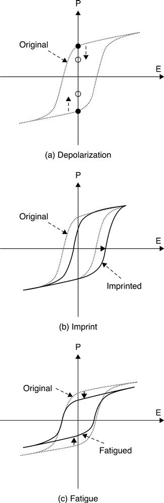
Electrical degradation phenomena of ferroelectric capacitor are typically classified into three categories, ‘depolarization,’ ‘imprint’ and ‘fatigue. These degradations are observed as an abnormality of P-E hysteresis (Fig. 14.9). Depolarization is observed as Pr decreases from the original (Fig. 14.9(a)). Imprint is observed as hysteresis shifts from the original position (Fig. 14.9(b)). For example, P-E hysteresis shifts to the + direction after storing the ‘1’ state. Fatigue is observed as hysteresis shrinks from the original (Fig. 14.9(c)). Many researchers have investigated the root cause of these degradations. Charged defects, such as oxygen vacancy or its related defects, are believed to induce these types of degradation.8,73,74
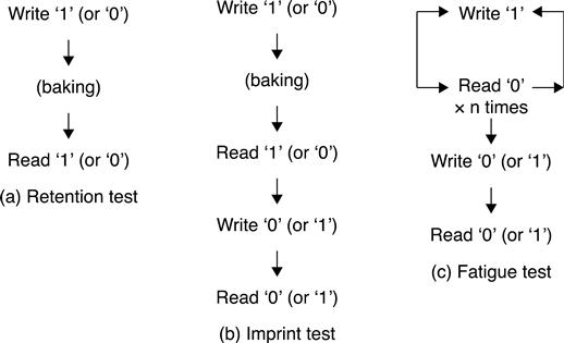
For highly reliable mass production of FRAM, a suitable testing procedure is important for examining the above-mentioned degradation of ferroelectric capacitors. A retention test, which consists of writing, storing and reading stored data (Fig. 14.10(a)), checks the ability of the ferroelectric capacitor to retain the initial stored data. If the ferroelectric capacitor is degraded by depolarization, the data reading operation may fail in this test. An imprint test checks the ability of a ferroelectric capacitor to rewrite the stored data as opposite data, for example, writing and storing ‘1’ and then rewriting the stored ‘1’ as ‘0’ (Fig. 14.10(b)). This test consists of writing data, storing initial data, rewriting the opposite data and reading the rewritten data. If the hysteresis of the ferroelectric capacitor shifts (Fig 14.10(b)), the reading operation of the rewritten data may fail in this test, because rewriting the opposite data becomes difficult due to an increase in Ec. A fatigue or a switching retention test checks the read/write function of ferroelectric capacitor after repetitions of ‘0–1’ switching (Fig 14.10(c)). The switching capability of commercialized FRAMs is larger than 1013, which is more than 107 times larger than that of Flash memory.
14.7 Applications of FRAM devices
In terms of memory application, commercialized FRAMs can be divided into two categories, stand-alone FRAM and embedded FRAM. While the former are only tested for memory functionality and are aimed at general customers, the latter are aimed at specialised customers.
Stand-alone FRAM with memory densities from a few Kb to a few Mb are commercially available. Conventional EEPROMs are often replaced by FRAMs to reduce power consumption and to improve the read/write performance. For example, stand-alone FRAMs are used for memories in electric power meters, which require multiple data rewriting per second. EEPROM cannot be used for this application because of shortage in rewriting capability (< 105). Battery-backed SRAMs are also often replaced by FRAMs, which is very advantageous because battery-free memory is not only cost-effective but also good for the environment. FRAMs are also applied to office automation and in automotive applications for their data logging, the purpose of storing engineering data, because of their high speed read/write and rewriting capabilities.
There are various types of FRAM-embedded LSIs, such as advanced smart cards, radio frequency identification (RFID) tags and authentication LSIs. Because of lower FRAM power consumption, greater communication distances can be achieved in wireless applications between card/tag and reader/writer. In addition, FRAM is suitable for authentication uses of smart cards or RFID tags, because strong encryption systems can be used due to its high speed read/write properties. FRAM is known to have a much higher resistance to gamma-ray irradiation than DRAM, EEPROM and Flash memories because FRAM does not store information as electric charges, which are significantly influenced by gamma rays.75 Therefore, FRAM can be employed for the RFID tags attached to medical equipment that is sterilized by gamma-rays.
14.8 Conclusion and future trends
FRAM is the first commercialized memory among advanced non-volatile memories such as MRAM, PRAM and ReRAM, though scalability remains one of its most important challenges. The International Technology Roadmap for Semiconductor (ITRS) 2012 predicts FRAM technology evolving to 90 nm nodes, a capacitor size of 0.32 μm2 and operational voltage of 1.2 V, a rather pessimistic prediction. However, with only a small evolution in comparison with other advanced semiconductor devices, and with the recent significant progress made in ferroelectric materials and FET-type FRAM material development, as described above, FRAM has the potential to overcome its scalability problems and exceed the ITRS predictions.