
Spin-transfer-torque magnetoresistive random access memory (STT-MRAM) technology
H. Ohno, T. Endoh, T. Hanyu, Y. Ando and S. Ikeda, Tohoku University, Japan
Abstract:
This chapter deals with magnetoresistive random access memory (MRAM) technology based on spin-transfer torque (STT) and the prospect of new directions in very-large-scale integrated circuits (VLSIs) made possible by the technology. Current materials and device technology using STT are first reviewed, with emphasis on magnetic tunnel junctions (MTJs) having perpendicular easy axis for magnetization. Then, STT-MRAM realizations based on the MTJ technology are explained; one for high density and the other for high speed, aiming at non-volatile main memory and high speed storage, and at non-volatile cache memory, respectively. Finally, non-volatile MTJ-based logic-in-memory architecture is shown to be capable of realizing both compactness and low power in a number of applications.
Key words
spin-transfer-torque; magnetic random access memory (MRAM); spintronics; integrated circuits; magnetic tunnel junction
15.1 Introduction
This chapter discusses non-volatile magnetoresistive random access memory (MRAM) technology based on spin-transfer torque (STT). It reviews new directions in very-large-scale integrated circuits (VLSIs) made possible by the technology. The increase in both power consumption and interconnection delay are two challenges that need to be addressed, in order to enhance the performance of the next-generation of VLSIs. The use of high performance non-volatile memory in the back-end-of-line process (BEOL) of VLSI is expected to result in reductions of both power consumption and interconnection delay. The non-volatile memory suitable for VLSI applications needs to have features of access time of less than 10 ns, virtually unlimited endurance and a scalable writing scheme at a small dimension comparable to the corresponding CMOS technology node. STT-MRAM technology is being developed to meet these requirements. In this section, current materials and device technology using STT are reviewed with particular emphasis on magnetic tunnel junctions (MTJs) having perpendicular easy axis for magnetization utilizing interface perpendicular anisotropy at CoFeB-MgO. The development of STT-MRAM devices based on MTJ technology is discussed:
• a high density device characterised by non-volatile main memory and high speed storage;
• a high speed device characterised by non-volatile cache memory.
Finally, non-volatile MTJ-based logic-in-memory architecture is shown to be capable of realizing both compactness, resulting in reduced interconnection delay, and low power consumption in a number of applications. Future trends as well as further reading for interested readers are presented in the last part of this section.
15.2 Materials and devices
Non-volatile memory suitable for VLSI memory applications needs to have an access time of less than 10 ns, virtually unlimited endurance and scalable write-scheme, all at a small dimension compatible with the associated CMOS technology node. Magnetic tunnel junctions (MTJs) with spin transfer torque (STT) switching (Ohno et al. 2010) are being developed to satisfy these requirements. This sub-section reviews the materials and device technology for MTJs used in:
• prototype magnetoresistive random-access memories (MRAMs) (Chung et al. 2010; Hosomi et al. 2005; Kawahara et al. 2008; Kishi et al. 2008; Kitagawa et al. 2012; Slaughter et al. 2012; Takemura et al. 2010; Tsuchida et al. 2010; Worledge et al. 2010);
• logic circuits with embedded MTJs (Matsunaga et al. 2008, 2011, 2012a, 2013; Mochizuki et al. 2005; Natsui et al. 2013; Ohno et al. 2010; Ohsawa et al. 2012a, 2013a; Suzuki et al. 2009; Zhao et al. 2009).
Figure 15.1(a) shows a schematic diagram of a typical memory cell consisting of a MTJ-one transistor in STT-MRAM. An MTJ consists of two ferromagnetic electrode layers separated by a tunnel barrier. One of the two magnetic layers is called a recording layer, in which information is stored as the direction of magnetization. The other layer, called a reference layer, is engineered in such a way as to maintain a fixed magnetization direction. The resistance of a MTJ is different between the parallel (P) and anti-parallel (AP) configurations of the magnetization directions of the two magnetic layers.
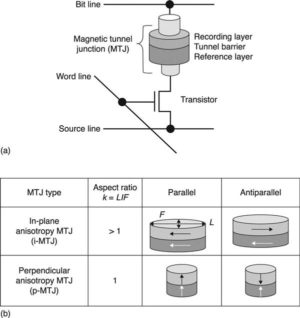
MTJs are classified into two types, depending on the direction of magnetic easy axes of the two magnetic layers. A magnetic easy axis is the direction in which magnetization assumes the lowest energy. The two types are:
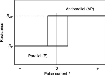
These two types are shown in Fig. 15.1(b). Unless an electrode material has crystalline perpendicular anisotropy, which is strong enough to overcome in-plane shape anisotropy, MTJs exhibit in-plane easy axis. Read and write operations are performed by applying low current to interrogate the resistance of the MTJ and by applying high current above the threshold current for switching, respectively. The MTJ is selected by the bit line and word line connected to a transistor (Fig. 15.1(a)). Magnetization switching of a recording layer by STT writing results from transfer of spin angular momentum from conduction electrons to the magnetization of the recording layer (Albert et al. 2000; Berger 1996; Katine et al. 2000; Mayer et al. 1999; Slonczewski 1996; Tsoi et al. 1998). P or AP configuration can be selected by the polarity of the write current through the target MTJ (Fig. 15.2). The resistance difference between the two magnetization configurations (A and AP) is a result of spin-dependent tunneling, which conserves spin direction. Consequently, the conduction depends on the density of states available at the Fermi energy for the majority and minority spin states and hence density-of-states spin polarization. This resistance change is defined as tunnel magnetoresistance (TMR) ratio = ΔR/R = (RAP − RP) /RP, where RAP and RP are the resistance for AP and P magnetization configurations (Fig. 15.1(b)), respectively.
Julliere (1975) found the TMR ratio was 14% at 4.2 K in the Fe/Ge(-O)/Co junction. Maekawa and Gafvert (1982) showed correspondence between the magnetization configuration and the resistance of the device at low temperatures in Ni/NiO/(Ni, Fe, or Co) junctions. In 1995, TMR ratios of more than 10% at room temperature (RT) were reported independently in amorphous Al-O barrier MTJs by Miyazaki and Tezuka (1995) at Tohoku University and Moodera et al. (1995) at MIT. The TMR ratio in Al-O barrier MTJs has increased year by year and reached 70%, which is close to the limit of the TMR ratio expected from the spin polarization at the Fermi energy. Butler et al. (2001) and Mathon and Umerski (2001) showed theoretically that TMR ratios can reach 100, to even 1000%, based on first-principles electronic structure calculations on fully ordered (001) oriented Fe/MgO/Fe MTJs.
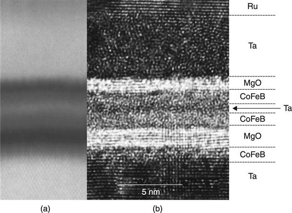
These predictions were later confirmed experimentally for fully (001) epitaxial Fe/MgO/Fe MTJs prepared using molecular beam epitaxy by Yuasa et al. (2004a,b) and for CoFe/MgO/CoFe MTJs prepared using a combination of ion-beam and magnetron sputtering by Parkin et al. (2004). Djayaprawira et al. (2005) and Hayakawa et al. (2005) demonstrated a TMR ratio of over 200% for MgO barrier i-MTJs with sputtered Co60Fe20B20 and Co40Fe40B20, respectively. The CoFeB/MgO MTJs are especially important from a mass-production point of view, because they are deposited on thermally oxidized Si using a conventional sputtering method and then annealed to attain high TMR. TMR ratios of up to 604% at RT, approaching the theoretically predicted value, have been observed in CoFeB/MgO barrier MTJs (Ikeda et al. 2008; Lee et al. 2007; Hayakawa et al. 2006; Yuasa et al. 2006). Figure 15.3 is a cross-sectional transmission electron microscope (TEM) image of high-TMR CoFeB-MgO barrier MTJ structure with bcc (001) oriented CoFeB electrodes and MgO (001) barrier for the coherent tunneling of Δ1 band electrons.

MTJs for VLSI application need to satisfy the following requirements:
1. a small size (F nm, where F represents the feature size);
2. a low current for STT write (the rule of thumb is critical switching current IC < F μA, because of the transistor drivability);
3. a high TMR ratio for fast sensing (> 100%);
4. a high thermal stability factor of the recording layer Δ = E/kBT (> 60, where E denotes the energy barrier between P and AP configurations, kB the Boltzmann constant and T the absolute temperature); and
5. capability to withstand annealing at 350 to 410 °C for BEOL post annealing, without losing its high TMR ratio.
The switching current IC for coherent magnetization reversal in i-MTJ and p-MTJ can be expressed as
[15.1]
[15.2]
where JC is the critical switching current density, A is the junction area, α is the magnetic damping constant, e is the elementary charge, MS is the saturation magnetization, t is the recording layer thickness, ħ is the reduced Planck constant, g(θ) is a function of the spin polarization of the tunnel current and the relative magnetization angle between the recording and the reference layers, HK is the anisotropy field that represents crystalline anisotropy, Hext is the external field, HKeff is the effective anisotropy field that includes both crystalline and shape anisotropies, and V (= At) is the volume of recording layer (Butler et al. 2001; Ikeda et al. 2010; Mangin et al. 2006; Mathon and Umerski 2001; Yoda et al. 2010). p-MTJs can achieve lower IC and higher Δ than i-MTJs, because IC is reduced by the demagnetizing field component and reduced junction area (A ∝ kF2, Fig. 15.1(b)), while Δ can be increased using high magnetic anisotropy materials. For this reason, STT-MRAMs with p-MTJs are being developed (Chung et al. 2010; Ikeda et al. 2010; Kishi et al. 2008; Kitagawa et al. 2012; Tsuchida et al. 2010; Worledge et al. 2010).
To attain perpendicular anisotropy, a number of material systems were explored as a recording layer material, including rare-earth/transition metal alloys (Cabrera et al. 2007; Nakayama et al. 2008; Nishimura et al. 2002; Ohmori et al. 2008) and L10-ordered (Co,Fe)-Pt (Kim et al. 2008; Yoda et al. 2010; Yoshikawa et al. 2008), as well as multilayers (Ishikawa et al. 2013; Mizunuma et al. 2009, 2011; Yakushiji et al. 2010a,b). For example, STT switching with 4.7 MA/cm2 in 130 nm-diameter TbFeCo/CoFeB/MgO/CoFeB/TbFeCo p-MTJ with Δ of 107 was reported, although the TMR ratio showed a value of 15% (Nakayama et al. 2008), mainly due to the lack of annealing tolerance. It was also found that 50 nm ϕ p-MTJs with Fe alloy doped with Pt and/or other elements resulted in a switching current of 10 μA and Δ of 32, although the TMR ratio showed a low value of 23% (Yoda et al. 2010). It turned out that conventional perpendicular materials examined do not satisfy the requirements for VLSI applications at the same time. This is understood in the following way; to realize a high TMR ratio a (100) CoFeBMgO-CoFeB structure is needed, but adding the structure to an electrode material with perpendicular anisotropy that is incompatible with the (001) structure results in either destruction of the (001) structure after annealing (hence low TMR) or the Mst value (Eq. (2)) being too large to observe switching.
In 2010, a perpendicular magnetic easy axis in Ta/CoFeB/MgO stacks with an ultra-thin CoFeB layer was developed, where CoFeB-MgO interface anisotropy was responsible for the anisotropy (Endo et al. 2010; Ikeda et al. 2010; Kanai et al. 2011; Yamanouchi et al. 2011). According to the first-principles calculation, the interfacial perpendicular anisotropy between oxide and ferromagnetic metal has its origin in the hybridization of Fe 3d and O 2p orbitals (Shimabukuro et al. 2010). Good TMR and STT properties of CoFeB-MgO p-MTJs were reported soon after the initial report. This approach is particularly suitable for p-MTJ, because no additional material is required other than CoFeB-MgO, a crucial materials combination for realizing a high TMR ratio (Ikeda et al. 2010). Figure 15.4(a) shows a schematic diagram of typical CoFeB-MgO p-MTJ. The junction diameter in the CoFeB-MgO p-MTJ is identified from a top view (Fig. 15.4(b)) taken by a scanning electron microscope and is 40 nm. The MTJ structures consist of, from the substrate side, Ta(5)/Ru(10)/Ta(5)/Co20Fe60B20(1.0)/MgO(0.85)/Co20Fe60B20(1.7)/Ta(5)/Ru(5) (numbers in parenthesis are nominal thicknesses in nanometers).
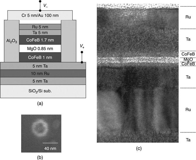
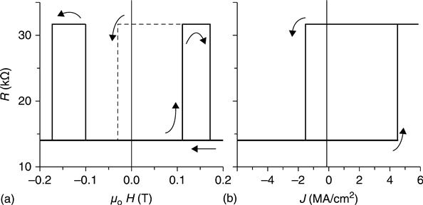
Figure 15.4(c) is a cross-sectional TEM image of the p-MTJ annealed at 300 °C. This confirms that the top and bottom CoFeB layers and MgO barrier are also continuous in the thickness of nm order. Figure 15.5(a) shows major and minor loops of the out-of plane resistance vs field (R-H) curve in the CoFeB-MgO p-MTJ with 40 nm in diameter annealed at 300 °C. The TMR ratio is 124% with resistance area product RA = 18 Ωμm2. In addition, no degradations of the TMR ratio and RA were observed after annealing at 350 °C. Figure 15.5(b) shows the resistance vs current density (R-J) curves measured at a current-pulse duration τP = 300 μs, without an external magnetic field. Clear switching is observed at a current density of a few MA/cm2.
For p-MTJs with a single CoFeB-MgO interface, Δ shows a nearly constant value down to a critical junction size below which Δ starts to reduce. This constant value of Δ is a result of nucleation-type reversal (Sato et al. 2011), where a nucleation embryo having a size and length scale determined by material parameters governs the magnetization reversal, and sets the highest attainable Δ of a stack. It is also found that Δ increases linearly as the thickness of the recording layer increases (Sato et al. 2012a), until the junction size is larger than the critical size of the nucleation embryo. It is therefore necessary to increase the thickness of the recording layer, increasing the contribution of in-plane anisotropy, while maintaining the perpendicular easy axis. To realize this, a double CoFeB-MgO interface structure was adopted to increase the interface anisotropy (Sato et al. 2012b).
It has been shown that the double-interface MgO/CoFeB/Ta/CoFeB/MgO recording structure in p-MTJs having a synthetic ferromagnetic (SyF) reference layer (Fig. 15.6) increases Δ by approximately 60 at a dimension of 29 nm in diameter, while keeping comparable intrinsic critical current density compared to the single interface CoFeB-MgO recording structure (Sato et al. 2013). This can be understood by a decrease of α increasing the total CoFeB recoding layer thickness (Ikeda et al. 2010). A fast switching speed by STT (Worledge et al. 2011), low write error rate (Nowak et al. 2011) and high endurance (Yoshida et al. 2012) have also been demonstrated in p-MTJ with a single interface CoFeB-MgO recording structure. Consequently CoFeB/MgO interfacial anisotropy technology is becoming an indispensable building block in developing non-volatile STT-MRAM for VLSIs.
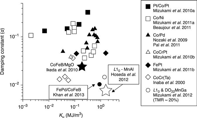
It should be noted that a trade-off exists between write current IC and thermal stability Δ (Eq. (2)). Current CoFeB-MgO interface anisotropy technology appears to take us to the beginning of a 1X-nm generation. In order to scale down the device dimension further, the switching current and device dimension need to be reduced while maintaining a required E, i.e. Δ. This requires development of perpendicular anisotropy electrode materials with high anisotropy and low α. Based on recent experiments, there is an empirical correlation between saturation magnetization and the damping parameter α. The saturation magnetization of L10-MnAl is a half value of that of CoFeB. It has been shown that high-quality MnAn films with a surface roughness of 0.4 nm, an important factor for obtaining a high TMR ratio, exhibit a high anisotropy of 1 × 10⁶ J/m3 with low saturation magnetization of 0.67 T and a damping parameter α of 0.003; it is 1/10 in comparison with that of CoFeB (Fig. 15.7) (Hosoda et al. 2012).
15.3 Improving memory storage
A lot of power is consumed in facilities such as data centres, not only by the computers themselves but also by the systems for conditioning air whose temperature is raised by the heat generated by the computers. The main reason attributed to the increase in computer operating power is leakage of current from semiconductor integrated circuits due to the device scaling. Figure 15.8(a) represents the state-of-the-art computer memory hierarchy in which working memories such as SRAM cache and DRAM main memory are volatile. By scaling the feature sizes of MOSFETs consisting of the memories, the sub-threshold leakage increases exponentially, causing a large increase in static current leakage in SRAMs. The speed gap between the SRAM cache and the DRAM main memory and that between the DRAM main memory and the storage (SSD, HDD) are another bottleneck in the computer’s performance gain by scaling.
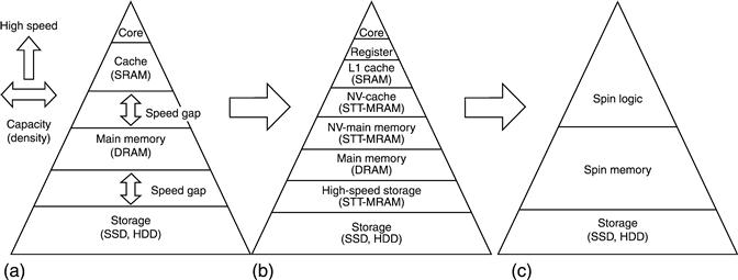
Figure 15.8(b) suggests a possible new memory hierarchy where the last level (LL) cache is constructed by non-volatile STT-MRAMs and the two speed gaps are filled with non-volatile (NV)-main memory and high-speed storage to boost performance, both being based on STT-MRAMs (Endoh et al. 2012). This structure can solve the power problem, because the large static current leakage can be eliminated by shutting down the power supply of the non-volatile cache memory when it is idle. The use of STT-MRAM in non-volatile (NV)-main memory as DRAM cache and in high-speed storage as storage cache is also effective in resolving the speed-gap problem. Figure 15.8(c) depicts the next step, an extreme non-volatile computer system. In this second generation, logic is also made non-volatile by using spintronics.
15.3.1 Non-volatile MRAM for main memories
A memory cell consisting of an MTJ and a metal-oxide semiconductor field-effect transistor (MOSFET) as the MTJ’s selective device can achieve a high-density memory aimed at a non-volatile main memory. Figure 15.9(a) illustrates a conventional one transistor and one MTJ (1T1MTJ) cell, in which the MOSFET is the n-type (NFET). The bottom layer (closer to the silicon surface) of an MTJ is usually the pinned layer. In this configuration, the current IUP that flows from the bottom pin to the top pin to switch the MTJ from parallel state to anti-parallel state is reduced because the NFET operates in the saturation region. The current IDOWN that flows from the top pin to the bottom pin to switch the MTJ from anti-parallel state to parallel state can be larger than IUP. However, it is also usual that the critical current needed to switch an MTJ from parallel to anti-parallel IC0 is larger than the critical current required to switch the MTJ from anti-parallel state to parallel state ICI. Therefore, the asymmetry of the MOSFET current drivability in IUP and IDOWN is not consistent with the asymmetry of the MTJ critical currents IC0 and ICI, making the switching difficult. The inconsistency can be resolved either by reversing the connection by wiring (Lin et al. 2009) or by making the MTJ top-pinned (Lee 2010). However, the former method increases the cell size and the latter introduces a difficulty into the process.
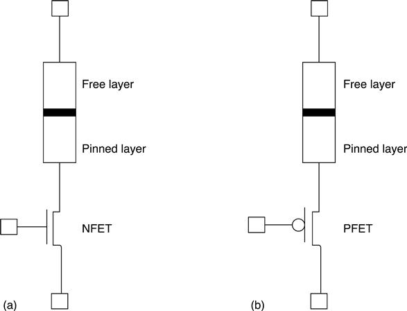
A 1T1MTJ memory cell using a p-type MOSFET (PFET) as the selective device has also been shown to be a solution resolving the asymmetry (Fig. 15.9(b)) (Koike and Endoh 2011). By using a PFET as the MTJ selective device, the asymmetry of the MOSFET current drivability can be consistent with the asymmetry of the MTJ critical current without changing the bottom-pin process, making both the switching and the process easier. Figure 15.10 shows the relationship between the currents NFET and PFET can flow and the MTJs critical currents in switching for both directions. This shows that the NFET cannot flow a large enough current to switch the MTJ from parallel to anti-parallel, while the PFET can flow large enough currents to switch the MTJs for both directions.

The 1T1MTJ cell of the present day is larger than the 1T1C DRAM cell used in main memories, because the critical currents required in switching MTJs are still large because of the relatively large junction size. However, since it has been shown that the critical currents for MTJ switching are reduced according to D2 (D = MTJ diameter), the currents can be reduced drastically by scaling the MTJ size. This current reduction contributes to the reduction in the channel width of the selective transistor in the 1T1MTJ cell, making the 1T1MTJ cell much smaller. It is roughly estimated that the channel width of the selective transistor of an 1T1MTJ cell can be as small as the minimum feature size F, if the diameter of MTJ is reduced to D = 25 nm in F = 22 nm technology node and that the 1T1MTJ cell size can match the 1T1C DRAM cell.
Furthermore, given that scaling F to 20 nm or smaller becomes difficult in DRAM, due to its capacitor scaling issue, the 1T1MTJ cell may replace the 1T1C DRAM cell in 20 nm node and beyond. Another advantage of the 1T1MTJ cell over the 1T1C DRAM cell in terms of integration density is that the constraint on the switching transistor in the 1T1MTJ cell is much more relaxed than that on the DRAM switching transistor. DRAM switching transistor must satisfy both the large current drivability and the very small cut-off current to retain the charge stored in the capacitor for more than a few seconds at high temperature for an average cell. The switching transistor of the 1T1MTJ cell, on the other hand, has no severe constraint on the cut-off feature. This difference also means that the channel length of 1T1MTJ cell can be smaller than the 1T1C DRAM cell in 20 nm technology node and beyond, thereby achieving a smaller cell size.
15.3.2 Non-volatile MRAM for cache memories
Although the 1T1MTJ cell can provide a high-density non-volatile memory suitable for a main memory, its access time is not fast enough to be applied to cache memories (Takemura et al. 2010). One major reason is that a reference current or voltage is required to sense the data that is read from the 1T1MTJ cell. In general, generating an accurate reference current or voltage on a chip is very difficult (Ohsawa et al. 2011a). MTJ-based differential pair type cells have been proposed in high-speed applications (Abe et al. 2010; Yamamoto and Sugahara 2009). They need no reference current or voltage for the data to be read by a sense amplifier, because the read is double-ended in the sense that a pair of true and complement signals are read from the cells. Therefore, access times are expected to be much faster than that of the 1T1MTJ cell. However, they have six or more MOSFETs in addition to two MTJs, making the cell size larger than the conventional SRAM.
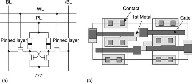
To overcome the large cell size, a 4T2MTJ cell has been proposed that has the potential to become smaller than the conventional SRAM cell (Ohsawa et al. 2011b; 2012a) (Fig. 15.11(a)). Two PFETs in the conventional SRAM cell are replaced by a pair of MTJs. The pinned layers must be connected to the power line (PL) for the cell to be read non-destructively. The operation of the cell is very similar to the SRAM, the only difference being that PL is clocked low and high to switch the two MTJs to the opposite states. Figure 15.11(b) shows the cell’s physical layout; only four NFETs are drawn in the figure. Two MTJs in the cell can be put on the drain areas between the two gates. Since the cell’s footprint is determined by the four NFETs, the cell can be smaller than the SRAM cell if the channel widths of the MOSFETs are as small as those in the SRAM. It was predicted that the cell size can become smaller than the SRAM in 45 nm technology node and beyond by scaling the thickness of the tunnel dielectrics (MgO) of the MTJs along with their areas (Ohsawa et al. 2011b, 2012a).
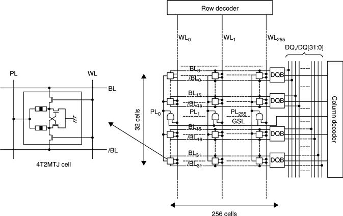
To reduce the power consumption in memories using the 4T2MTJ cell, it is important to control PL according to the cell’s operational modes, because the cell consumes a static current between PL and GND through the MTJ in the anti-parallel MTJ. A fine-grained power gating scheme has been proposed to achieve a low-power and high-performance memory (Ohsawa et al. 2012b, 2013a). In this scheme, the PL of 32 cells along a word line (WL) are connected together to be controlled by a PL driver (Fig. 15.12). The PL driver is CMOS AND-type one that drives PL high and low in correspondence to WL from a row decoder and grain select signal (GSL) from a column decoder. When cells are to be written or read, the corresponding 32b-cell group (grain) is activated by raising PL high. It is worth noting that almost all other grains remain inactive with PL low, limiting the static current to that by the activated grain. Thus the fine-grained power gating scheme can reduce the power drastically in contrast to SRAM, in which all cells consume static current leakage. The fine-grained power gating scheme also has the merit of achieving fast wake-up and power-off times, realizing fast access and cycle times of memory. The number of cells controlled by a PL driver (grain size) needs to be determined in the trade-off between the operation power and the array size. The operation power increases as the grain size increases, because the static current that flows in the activated grain increases as the grain size increases.
On the other hand, the array size increases as the grain size decreases, because the area overhead of the PL drivers increases as the grain size decreases. The size 32 was an optimized number in the trade-off for the CMOS AND-type PL driver. Figure 15.13 shows the photo-micrograph of a 1 Mb STT-MRAM using the 4T2MTJ cell with the 32 b fine-grained power gating scheme that was fabricated in 90 nm CMOS and 100 nm perpendicular MTJ processes. The memory cell size is 2.19 μm2 and the 1 Mb macro size is 3.54 mm2. The functionality of the cells has been confirmed by using a simple write/read test pattern. The cell size is about twice as large as the SRAM cell counterpart in 90 nm technology node. This is due to the large MTJ critical currents in switching in 100 nm MTJ size. The channel width of the MOSFETs in the 4T2MTJ cell must be large enough to supply the critical currents. It was shown that the channel width divided by the channel length can be reduced by scaling the MTJ size. Therefore, the 4T2MTJ cell size can be smaller than the SRAM counterpart in 45 nm technology node and beyond, by scaling together with the MgO thinning, as mentioned previously.

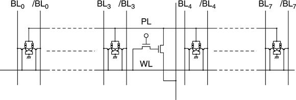
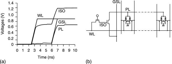
The CMOS AND-type PL driver that was used in the 32 b grain is not compact enough to be applied to a much smaller grain. A single MOSFET is not suitable for the PL driver for the 4T2MTJ cell, because PL voltage must be driven both high and low (PL needs to be low when one of the two MTJs is to be switched from parallel to anti-parallel). To overcome this, a two-transistor bootstrap-type PL driver consisting of only two NFETs (Ohsawa et al. 2013b) has been proposed. Figure 15.14 illustrates an 8 b grain with 4T2MTJ cells controlled by the two-transistor bootstrap-type PL driver. The PL driver has only two NFETs, one working as a driver to drive the PL line and the other working as a barrier transistor that is cut off to boost the voltage in the isolated gate of the driver NFET beyond the power supply voltage Vdd through the gate-channel capacitance of the driver NFET, to avoid the driver NFET operating in saturation region (Fig. 15.15). This PL driver is very compact and can drive PL high and low efficiently, being suitable to control a smaller grain.
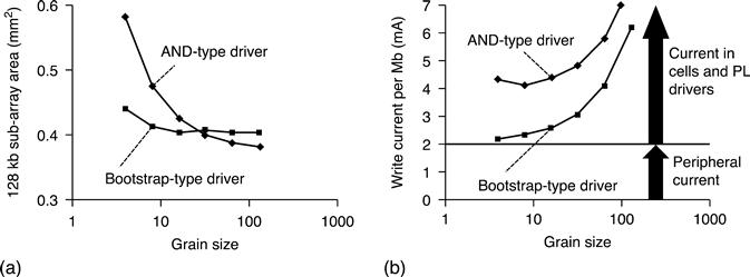
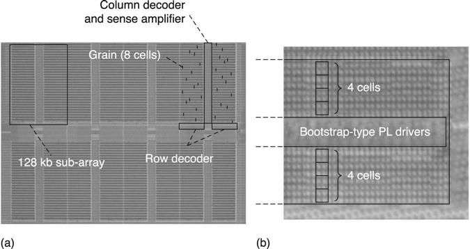
Another merit of using this two-transistor bootstrap-type PL driver is that the driver itself does not consume a static current due to sub-threshold leakage, unlike the CMOS AND-type PL driver. As a circuit unit, the number of PL drivers is the largest next to the memory cells, especially when the grain size is small. Therefore this static power is not negligible. Figure 15.16 compares the 128 kb sub-array area and the 1 Mb write current for the CMOS AND-type PL driver and the two-transistor bootstrap-type PL driver as a function of grain size. Figure 15.17(a) shows the photo-micrograph of a 1 Mb STT-MRAM using a 4T2MTJ cell with an 8 b super-fine-grained power gating scheme, in which two-transistor bootstraptype PL drivers are used. The magnified view for a 2 kb unit that includes 8 b grains is shown in Fig. 15.17(b), each of the grains having four cells in both sides of the PL driver (8 cells in total). The cell efficiency remains high (59%), even though the macro adopts a super-fine-grained power gating scheme of 8 b grain, due to the compact PL driver with only two NFETs.
Though MTJ has strong potential to be used in high-performance non-volatile working memories, one concern is that it requires a large current to switch it very quickly, namely in a few nanoseconds or faster (Aoki et al. 2008). The switching is also probabilistic when MTJs are to be switched by a moderate current (Diao 2007). To work around these issues, an auto-data back-up STT-MRAM with a background write scheme has been proposed (Ohsawa et al. 2013c). The general concept of the background write scheme for an auto-data back-up cell is illustrated in Fig. 15.18(a). There are two memories in a bit cell. Memories 1 and 2 have write times of tw1 and tw2 and retention times of tr1 and tr2, respectively. We assume that tw1 < tw2 and tr1 < < tr2. When a write cycle from outside through the switching FETs gated by WL is performed in a period t, so that tw1 < t < tw2, the data can be written to memory 1, but memory 2 is not written in the write period.
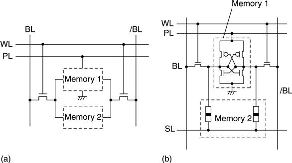
However, if memory 1 can switch memory 2 by using the data that is written to memory 1 for more than tw2, without control from outside or autonomously even after WL is lowered, memory 2 is also written without any help from outside. This auto-data back-up can be performed without interrupting the write operation specification in the memory chip, because the fast write cycles can be maintained with the relatively slow auto-data back-up performed in a manner that is hidden from the foreground write operation. This background write can achieve a memory cell with the write time tw1 and the retention time tr2. In Fig. 15.18(b), we adopted a CMOS latch as memory 1 and a pair of MTJ to achieve a non-volatile working memory cell with a fast write performance equivalent to SRAM.
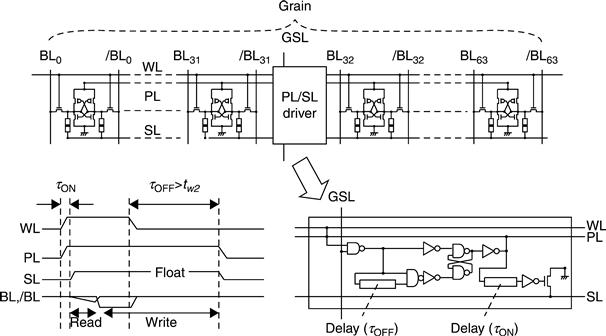
However, again, it is very important to shut PL down when the auto-data back-up operation is completed, to eliminate the static current that flows in the cell. Therefore, a timer that measures tw2 has been implemented into a PL driver used for a power gating scheme. Figure 15.19 shows the PL driver that controls a grain along a WL with its operational waveforms. The timing chart shows that PL activation is expanded to a longer period than tw2, to ensure that a pair of MTJs can be switched by using data written to a CMOS latch after WL is shut down. The PL driver includes two timers. One is for τOFF that measures tw2. The other is for τON that is a nanosecond or shorter, necessary for the data to be correctly loaded from a pair of MTJs to a CMOS latch. Figure 15.20 shows the photo-micrograph of a 1 Mb STT-MRAM using the auto-data back-up cell with a 64 b fine-grained power gating scheme, in which the PL driver in Fig. 15.19 is used to achieve the background write. It was fabricated in 90 nm CMOS and 100 nm perpendicular MTJ processes. The read and write cycle times are shown to be 1.5 and 2.1 nanoseconds by simulation respectively, fast enough to be applied to the LL cache.

15.4 Improving logic-in-memory architecture
Demand for high-performance and low-power logic LSIs has continued to increase, reflecting recent highly intelligent electronics applications. However, the increase in power dissipation, especially standby power dissipation, limits the performance in recent LSIs with nanometer-scaled transistors. This is caused by constant current leakage due to on-chip volatile memory modules such as static RAM and flip-flops. In addition, interconnection delay as well as power dissipation has to be managed to ensure LSIs are high in performance and low in power consumption. In order to counter such challenges in logic LSI, there are primarily two approaches:
1. utilizing a novel LSI architecture where intra-chip data transfer between memory and logic modules is localized as much as possible and global wire counts are minimized;
2. realizing a compact logic-LSI with a power-gating capability where the power supply to each fine-grained functional logic-circuit component can be shut down quickly (or turned on quickly) whenever its operation status changes to a standby mode (or comes back to an active mode again).
Approach (1) is achieved by utilizing a novel logic-LSI-oriented hardware structure, called ‘logic-in-memory (LIM)’ architecture (Kautz 1969). In the LIM architecture, storage elements are distributed over the logic-circuit plane to achieve low-power dissipation for data transmission and short interconnection delay, greatly reducing global interconnection wires.
In order to apply a power-gating technique (Approach (2)) in reducing the power dissipation of logic LSIs as efficiently as possible, every storage element must be non-volatile because stored data must remain even when the power supply is shut down by the power gating. MTJ with a spin-injection write capability has all the following features for such an application; a reasonably large resistance ratio, virtually unlimited endurance, fast read/write accessibility, scalability, complementary MOS (CMOS)-process compatibility and non-volatility. MTJ is thus suited to implement such an MOS/MTJ-hybrid logic circuit with LIM architecture (Mochizuki et al. 2005). Moreover, MTJ not only acts as a ‘storage element’, but can also be designed to act as a ‘logic element’, because its resistance is programmable in accordance with its stored status. This use of MTJ-based logic-circuit design allows the storage function to be merged into logic-circuit plane, resulting in a compact logic LSI (Matsunaga et al. 2008).
As a typical example of non-volatile logic-in-memory architecture, MTJ-based non-volatile Ternary Content-Addressable Memories (TCAMs) have been designed and fabricated (Matsunaga et al. 2011, 2012a,b,c, 2013, 2014). TCAM is a functional memory for high-speed data retrieval that performs a fully parallel search and fully parallel comparison between an input key and stored words. Currently, its high bit cost and high power dissipation, higher than those of standard semiconductor memories such as static random access memory, limits the fields to which TCAM can be applied. Table 15.1 shows the truth table of the TCAM cell function. Its rich functionality makes data search powerful and flexible, but with conventional CMOS realization there is an associated cost of a complicated logic circuit with two-bit storage elements.
Table 15.1
Truth table of the TCAM cell function
| Stored data | Search input | Current comparison | Match result | |
| B | (b1, b2) | S | ML | |
| 0 | (0, 1) | 0 | 1 (Match) | |
| 1 | 0 (Mismatch) | |||
| 1 | (1, 0) | 0 | 0 (Mismatch) | |
| 1 | 1 (Match) | |||
| X (don’t care) | (0, 0) | 0 | 1 (Match) | |
| 1 | 1 (Match) | |||
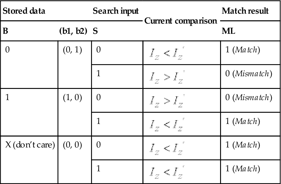
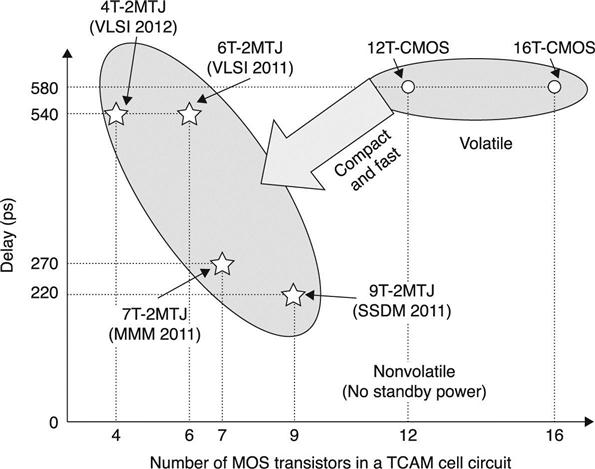
Figure 15.21 shows the design philosophy of realizing the TCAM cell circuit compactly with a non-volatile storage capability. In the case of both conventional volatile TCAM cell structure and conventional non-volatile TCAM cell structure without using LIM architecture shown in Figs. 15.21(a) and (b), respectively, the bit cost is high. In contrast, when two-bit storage elements are merged into a logic-circuit part, by using the LIM architecture (Fig. 15.21(c)), the proposed TCAM cell structure becomes compact and non-volatile (Fig. 15.21(d)). Figures 15.22(a) and (b) compare a conventional volatile TCAM cell circuit and the proposed non-volatile one. The conventional CMOS-based volatile TCAM cell circuit consumes 12 MOS transistors (12 T-TCAM circuit structure), while the proposed one takes just 4 MOS transistors with two MTJ devices (4 T-2MTJ circuit structure).
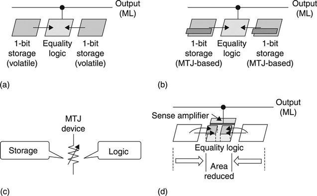

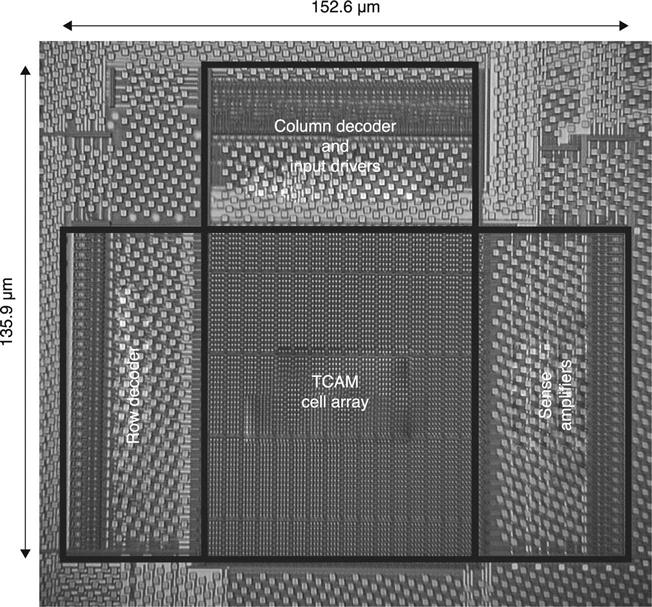
Note that MTJs do not affect the total TCAM cell-circuit one, because MTJs are fabricated onto the CMOS plane. Compact realization due to NV-LIM architecture has the advantage of improving the performance of the circuit by inserting a driver (Fig. 15.22(c)). Figure 15.23 summarizes the comparison of TCAM word circuits with 144 cells. By the appropriate division of the TCAM word circuit, the activation ratio of the TCAM can be minimized. Figure 15.24 shows the variety of the segment-based TCAM structures. In the case of the 3-segment-based NV-TCAM structure, where the first segment, the second-segment and the rest consist of 3-bit, 7-bit and 134-bit cells, respectively, its average activation ratio becomes as low as 2.8%, which indicates that 97% or more TCAM cells can be in standby mode on average by the fine-grained power gating. Figure 15.25 shows the fabricated non-volatile TCAM test chip under 90 nm CMOS and 100 nm MTJ technologies.

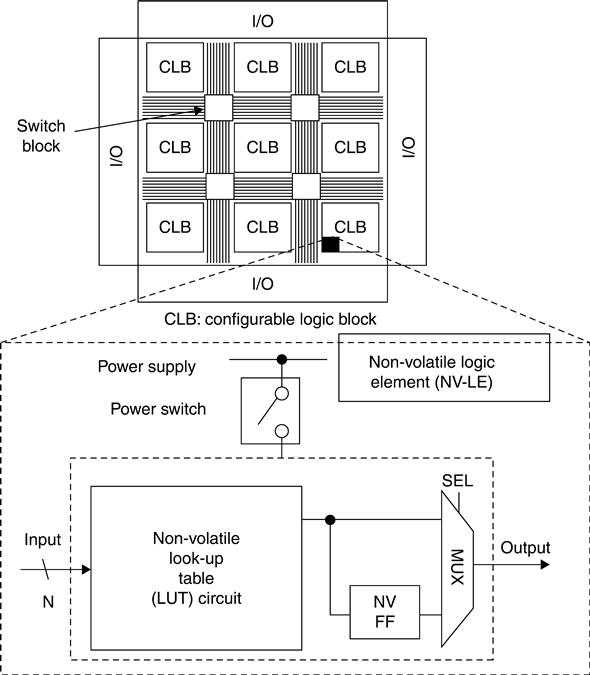
MTJ-based non-volatile look-up table (LUT) circuit for an instant power-ON/OFF Field Programmable Gate Array (FPGA) is another example that shows the clear advantage of non-volatile logic-in-memory architecture (Suzuki et al. 2009, 2012, 2013a,b, 2014). Figure 15.26 shows the overall structure of a non-volatile FPGA, where each LUT circuit in the configurable logic block (CLB) stores logical configuration data into non-volatile storage elements in the present case MTJs. Therefore, whenever an LUT circuit is in standby mode, its power supply can be shut down completely, eliminating the wasted standby power dissipation. Although the use of MTJs makes the LUT circuit non-volatile, its hardware cost is increased when volatile storage elements are replaced with non-volatile ones (Fig. 15.27(a)). To circumvent the hardware overhead in Fig. 12.27(b), MTJs are merged into the combinational logic circuit in the LUT circuit by using NV-LIM architecture, resulting in a highly compact LUT circuit; only a single sense amplifier (SA) is required in the proposed structure. Figure 15.28 shows a fabricated two-input non-volatile LUT-circuit test chip.


In practical FPGA, the LUT circuit must have four inputs or more. Since a multi-input LUT circuit requires many MTJs, the variation of the resistance values of MTJs becomes critical. For stable LUT operation of multi-input LUT circuits, additional MTJs can be added to adjust the operating point of the LUT function. Figure 15.29 shows an example where both two and three additional MTJs are inserted into the LUT-selection tree and the LUT-reference tree, respectively. Table 15.2 summarizes the comparison of 6-input LUT circuits. This clearly demonstrates that the proposed NV-LIM-based NV-LUT circuit is implemented compactly with shorter delay and less active power dissipation in comparison with those using the conventional approach.
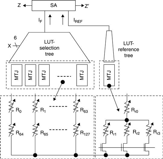
Table 15.2
Comparison of 6-input non-volatile LUT circuits
| CMOS-based* | Proposed | |
| Number of devices | 590 Tr. + 128 MTJ | 222 Tr. + 132 MTJ |
| Delay† | 194 ps | 150 ps |
| Active power at 1 GHz† | 7.43 μW | 5.72 μW |
| Standby power | 0 μW | 0 μW |
Notes: RP = 1.27 kΩ, RAP = 2.70 kΩ, IW1 = 112 μA, IW0 = − 180 μA.
*Composed of 64-bit MTJ-based non-volatile SRAM (448 Tr.), nMOS selector tree (126 Tr.), inverters (12 Tr.) and output buffer (4 Tr.).
†SPICE simulation under a 90 nm CMOS technology.
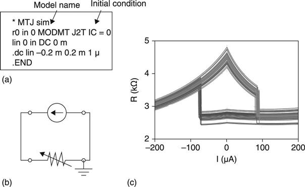
Finally, an MTJ-based non-volatile random-logic LSI with LIM architecture is discussed (Natsui et al. 2013; Sakimura et al. 2012). In designing such a large-scaled logic circuit with NV-LIM architecture, it is important to establish a semi-automatic LSI CAD tool. Figure 15.30 shows a circuit simulator, SPICE, where the MTJ device model with spin-transfer-torque write is built-in as one of the basic circuit components. A sub-circuit macro-model emulating MTJ characteristics were discussed previously (Harms et al. 2010; Kostrov 2010; Zhao et al. 2006) and its behaviour was simulated by importing it to the circuit simulator. However, it could not achieve sufficient simulation speed and accuracy, since the use of the complex sub-circuit model resulted in a high CPU time penalty. The proposed SPICE simulator incorporates MTJ model parameters and can perform accurate simulation of a complex circuit operation, including MTJ switching behaviour with a small computational cost. The proposed simulator achieves MTJ behaviour up to 50 times faster than with a conventional sub-circuit-based one. Figure 15.31 shows a layout-design example of an NV-LIM-based random logic circuit. All the NV-LIM-based circuit primitives are automatically generated in this design. Figure 15.32 shows a chip photo-micrograph of a hardware accelerator for motion-vector extraction. The number of PEs arranged in a 5 × 5 grid is 25. The number of MOS transistors is about 0.5 million and that of MTJ devices is about 13 000.


15.5 Future trends
This section discusses future directions on various fronts involved in STT-MRAM development.
15.5.1 Materials and devices
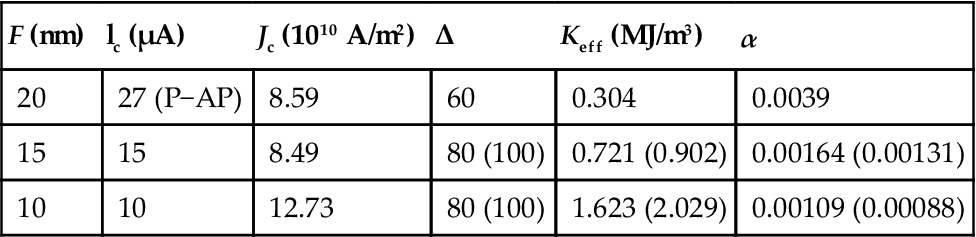
In order to scale the switching current for STT in an MTJ, a low α is required while maintaining high thermal stability. As shown in Table 15.3, Keff and α in double CoFeB-MgO MTJ with 20 nm ϕ and 2.6 nm-thick recording layer were calculated from Eq. 15.2, using the experimental values of IC, and Δ. When it is assumed that 10 nm ϕ and 15 nm ϕ MTJs can realize the IC of F μA and the heat stability of 80 to 100, the Keff and α were estimated from Eq. 15.2. The realization of both IC = F μA and Δ = 80 to 100 in the 10 (15) nm ϕ MTJs needs to increase Keff to 5.3–6.7 (2.4–3.0) times and decrease α to 1/4–1/5 (1/2–1/3), as compared with those of 20 nm ϕ MTJs.
Table 15.3
| F (nm) | lc (μA) | Jc (1010 A/m2) | Δ | Keff (MJ/m3) | α |
| 20 | 27 (P−AP) | 8.59 | 60 | 0.304 | 0.0039 |
| 15 | 15 | 8.49 | 80 (100) | 0.721 (0.902) | 0.00164 (0.00131) |
| 10 | 10 | 12.73 | 80 (100) | 1.623 (2.029) | 0.00109 (0.00088) |
L10-Mn-based alloys (i.e. MnGa and MnAl), which satisfy high thermal stability and low α at the same time, are capable of realizing such a recording layer (Hosoda et al. 2012; Kubota et al. 2012; Ma et al. 2012; Saruyama et al. 2013). In p-MTJs with a MnGa/MgO/CoFe(B) stack, a TMR ratio of 5% at RT was observed. Insertion of Fe or Co between Mn-based alloy and MgO helps increase the TMR ratio to 40% (Kubota et al. 2012; Ma et al. 2012; Saruyama et al. 2013). However, this is not high enough. In this system a further increase of the TMR ratio and demonstration of STT switching are the next steps. It is also necessary to perform an in-parallel search of other material systems with higher thermal stability and lower α for further dimension reduction of MTJ.
There are two approaches to construct a memory cell using MTJ devices. The 2-terminal cell such as STT-MTJ has the advantage of scalability for high density memory embedded in VLSIs. The 3-terminal cell utilizes domain wall motion by the spin-polarized current (Fukami et al. 2009, 2013) or spin hall effect (Liu et al. 2012; Pai et al. 2012; Yamanouchi et al. 2012) for write operation. The 3-terminal cell can increase the speed of operation over the 2-terminal cell, because the write and read paths are separated to avoid disturbance and is a particularly strong candidate for substitution of embedded SRAMs. Cell structures strongly affect performance, area efficiency and reliability of non-volatile memory and CMOS logic applications, consequently an optimized and perhaps combined approach is needed to satisfy the requirements of specific applications.
Write energy of current-driven write operation for the 2- and 3-terminal cells is still a few orders larger than switching CMOS. Therefore, along with developing schemes to reduce write energy, it is necessary to explore other write (magnetization switching) schemes to reduce the dynamic power of these devices. One possibility is to utilize an electric field, E, to control the magnetic anisotropy of magnetic layer in an MTJ. Electric field-control of magnetism through carrier density modulation, which was first demonstrated for III–V ferromagnetic semiconductors (Chiba et al. 2003, 2006, 2008, 2010; Ohno et al. 2000), has been applied to 3D transition-metal and its alloy ferromagnets (Chiba et al. 2011; Maruyama et al. 2009; Meng et al. 2012; Shiota et al. 2012; Wang et al. 2012; Weisheit et al. 2007). Recently, electric-field control of magnetism, such as the change of coercivity and magnetization reversal, has been experimentally shown on CoFeB-MgO p-MTJs, paving the way to an entirely new and energy efficient write scheme for MRAM and associated devices (Endo et al. 2010; Kanai et al. 2011, 2012, 2013).
15.5.2 Memory
It is predicted that a memory static power component, especially for LSIs used in portable devices, will increase year on year and will become a large portion of the total power consumption (ITRS 2011). The main part of the static power consumption comes from SRAM caches. The state-of-the-art memory hierarchy in computers is shown in Fig. 15.8(a), in which the caches’ capacities are increasing for improved performance. This is due to the sub-threshold leakage increase by the MOSFET channel length’s scaling in obtaining high-speed operation as well as high-density integration. Another problem is speed gaps in the memory hierarchy. One is between the SRAM cache and the DRAM main memory. The other is between the DRAM main memory and the storage. To solve the above issues, a new memory hierarchy based on non-volatile memories using STT-MRAMs was proposed (Fig. 15.8(b)). In Section 15.3, we presented circuit technologies realizing the STT-MRAMs that can be used in the new memory hierarchy. Furthermore, we propose an ultimate memory hierarchy (Fig. 15.8(c)), in which all working segments in the computers are made non-volatile by using spintronics. One of the key technologies in the spin logic is an MTJ-based non-volatile logic-in-memory (Ohno et al. 2010). In the architecture, MTJ-based non-volatile memory elements are distributed over the logic circuit to eliminate long wirings between memory and logic. The resultant effects expected are two-fold:
15.5.3 Logic
Further advancement of the non-volatile MTJ-based logic-gate families described in this chapter represent a rich future direction of achieving lower power yet higher performance logic VLSI. In addition, establishing design methods to automatically minimize the power-delay-area product in both general-purpose and special-purpose logic VLSIs is required. A wide variety of possibilities have just begun to surface.
15.6 Conclusion
This chapter has given an overview of the STT-MRAM technology. STT-MRAM has two advantages that have not been explicitly discussed. One is that the physics involved in switching and TMR is reasonably well established. The other is that there is a large research community of magnetism and magnetics, as well as an industrial community of hard disk drives. So it is already known, for example, that a non-volatile bit of less than 10 nm in diameter is possible due to the hard disk industry that has established it in the recording media. The materials science has to be developed for MTJs and their sister devices before it will be possible to scale MTJ deep into 1X nm and even beyond 10 nm. However, it is time to call for circuit-device collaboration as the performance of an MTJ has become reasonably high. Several examples are shown in this chapter which emphasize the advantage of non-volatility of MTJs and mask other shortcomings of current MTJ technology. This chapter also proposes that with virtually unlimited endurance and with its back-end-of-line compatibility, MTJs can be implemented as part of logic on a CMOS logic plane that can store information without the need for power. This demonstration of non-volatile logic-in-memory architecture opens up a number of new possibilities that could not be realized by CMOS alone. Several examples of logic-in-memory realization, not just design but in real chips, are included to emphasize this new possibility.
15.7 Acknowledgement
Part of the authors’ work described here has been supported by the project ‘Research and Development of Ultra-low Power Spintronics-based VLSIs’ through the ‘Funding Program for World-Leading Innovative R&D on Science and Technology (FIRST Program)’ by the Japan Society for the Promotion of Science (JSPS) initiated by the Council for Science and Technology Policy (CSTP) and ‘Research and Development of Spintronics Material and Device Science and Technology for a Disaster-Resistant Safe and Secure Society’ program under Research and Development for Next-Generation Information Technology of Ministry of Education, Culture, Sports, Science and Technology (MEXT). The authors thank Takashi Ohsawa and Naoki Kasai for their support.