
Memristors for non-volatile memory and other applications
G.M. Huang and Y. Ho, Texas A&M University, USA
Abstract:
Non-volatile memory technologies are essential for the next generation of nano-computing. This chapter highlights several key issues associated with non-volatile memory design based on the emerging memristor devices. In this chapter, an overview of commonly used memristor device models is provided, and a comprehensive set of properties and design equations for memristor-based memories are developed. The provided analyses are particularly targeting key memristor device characteristics relevant to memory operations. Finally, other promising applications of memristor devices are briefly discussed.
Key words
charge-controlled memristance; flux-controlled memristance; titanium-dioxide memristor; zero-net charge; zero-net flux
11.1 Introduction
The memristor is a device recognized as the first real-life realization of the so-called missing fourth circuit element introduced by Chua (1971). The name ‘memristor’ originates from the term ‘memory resistor’ (Chua 1971), which reflects the fact that memristors can store information in a non-volatile fashion. In late 2008, S. Williams, researcher at Hewlett-Packard (HP) laboratory, reported a memristor device, a two-terminal titanium dioxide, which displayed memristive hysteresis characteristics at the nano-scale. Kim et al. (2012) demonstrated that memristor devices can be scaled down to 10 nm or below and a memristor cross-bar array can achieve an integration density of 10 Gbits/cm2, which exceeds the density of today’s advanced Flash memory technologies. Furthermore, memristors can withstand up to a million write-cycles, whereas the Flash memory can only withstand about 100 000 write cycles (Bourzac 2010).
In this chapter, beginning with Section 11.2, the fundamental theory of memristor and the basic concept will be introduced. Most of the research works in the memristor area use the models proposed by the HP research group. The proposed HP memristor models can be categorized into the linear and nonlinear drift models. Section 11.2 will cover some of the commonly seen memristor models.
Although memristive memory has greater scale capability, the design of read/write topology and memory peripheral circuitries is challenging. The dynamic behavior of a memristor device will influence all aspects of design of memristor memories. Section 11.3 introduces a design method for memristor-based memory storage. The design flow has three basic steps:
1. systematically develop a complete set of properties and design equations for guiding the development of memristor based memories, and show important dynamical behaviors of memristor devices and how these characteristics will influence all aspects of analysis and design of memristor memories;
Lastly, Section 11.4 briefly showcases numbers of promising applications. Researchers have found that the memristor can perform implication (‘stateful’) logic, which is equivalent to the universal Boolean logic such as NAND and NOR. The memristor brings stateful logic operations for which the memristive devices function as logic gates that use resistance rather than charge or voltage as a physical state variable. Thus, it saves computational power in this sense. In the meantime, researchers have found that memristors can model adaptive behavior of unicellular organisms. Results show that electronic circuits with memristors subjected to a train of periodic pulses behave like brain functions, which are able to learn and anticipate. Such a learning circuit may find its valuable applications in a variety of areas, for example, neural networks and artificial intelligences (Linares-Barranco and Serrano-Gotarredona 2009; Pershin and Ventra 2009; Pershin et al. 2009; Sharifi and Banadaki 2010; Snider 2008).
11.2 The realization of memristor devices
11.2.1 Memristor theory
The fundamental basic circuit elements are resistor, capacitor and inductor. The resistor relates voltage and current (dv = R · di), the capacitor relates charge and voltage (dq = C · dv) and the inductor relates flux and current (dφ = L · di), respectively. Chua (1971) argued that there is a missing link between flux and charge, which he called memristance, M (Fig. 11.1).
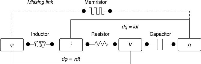
Basically, memristance defines the φ-q relation. It becomes resistance if the φ-q relation is linear. In general, memristance is defined as
and memductance is defined as
From Eqs 11.1 and 11.2, it can be also seen that
The memristance, M, is equivalent to voltage over current, which is also known as the resistance in the linear case. Therefore, memristance has the same unit (Ohm) as resistance, and the memductance has the unit of conductance (1/Ohm). The inverse of memductance is memristance, so
The memristor can be charge-controlled or flux-controlled. It is charge-controlled when charge is applied to the cell and changes its memristance. Similarly, the memristor is flux-controlled if the flux is applied and changes its memductance.
11.2.2 The memristor device models
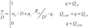
In 2008, HP demonstrated a fabricated physical structure of a memristor device, also known as the Titanium dioxide memristor. Strukov et al. (2008) showcase that the device is an electrically switchable semiconductor thin film sandwiched between two metal contacts. This titanium dioxide thin film consists of a doped and undoped region (Fig. 11.2(a)), and has a total length of D. The undoped region is composed of pure titanium dioxide (TiO2), which is highly resistive, and the doped region is filled with oxygen vacancies (TiO2-x), which makes it highly conductive. The internal state variable, w, is the length of the doped region. The doped region has low resistance, and the undoped region has high resistance. If a voltage potential is applied across the memristor, the doped/undoped region changes its size due to charged dopant drifting.

Accordingly, the electric field will repel positively charged oxygen vacancies in the doped layer into the pure TiO2 layer, resulting the length of w being changed, thus, the device total resistivity will be changed. The equivalent circuit model is shown in Figs 11.2(b), and Fig. 11.2(c) is the memristor circuit symbol used by Chua (1971). If the doped region extends to the full length D, that is w/D = 1.0, the cell will be dominated by low resistivity ions, and the total resistivity of the device will reach its lowest point (measured to be Ron). Likewise, when the undoped region extends to the full length D, i.e. w/D = 0, the total resistance reaches its highest point, denoted as Roff. Strukov et al. (2008) describe the mathematical model for memristive device resistance as
or can be written as
Due to the physical constraint 0 ≤ w ≤ D, the total resistance is bounded between Ron and Roff.
Figure 11.2(c) shows the memristor symbol used in a circuit schematic. The orientation of the symbol follows the equivalent circuit in Fig. 11.2(b). The polarity matters in a memristor cell, because if a bias condition increases the memristance, the reverse connection would decrease the memristance, which is also equivalent to reversing the polarity of the biasing source. Using this resistive viewpoint, it can be seen that
According to recent research results, there are two types of memristor models: linear drift model and nonlinear drift model.
Linear drift model
According to Strukov et al. (2008), the linear dopant drift model assumes linear ionic drift in a uniform electric field across the device. More specifically, the net electric field induced in a current flow through the memristor device is found to be linearly proportional to the drift-diffusion velocity. Since the drift-diffusion velocity corresponds to the speed of doped region (dw/dt), the following equation is established:
where μv is the average ion mobility.
Nonlinear drift model
According to the actual memristor device manufactured in the HP lab, the small voltage can yield a massive electric field, which produces significant nonlinear ionic transport. These nonlinearities appear to slow down the drift velocity at the thin film edges, where the speed of the state transition around the boundary gradually decreases. This nonlinear dopant-drifting phenomenon is the so-called boundary effect (Biolet et al. 2009; Joglekar and Wolf 2008; Kavehei et al. 2010; Wang 2008). One approach to model the boundary effect is by applying window function f(w) to the drift velocity equation:
A widely proposed window function introduced by Joglekar and Wolf (2008) is
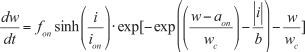
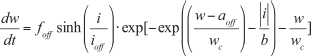
where P is the control parameter that needs to be matched to the manufactured memristor data. The control parameter can only be made up of positive integers. However, the theoretical models can go much deeper than just window functions. In late 2008, the research group at HP further announced that the memristive switch mechanism of a flux-controlled memristor can be described as (Yang et al. 2008)
where w is memristor state, V is the applied voltage, I is the current through memristor, and all others are fitting parameters. When the memristor is around Ron, Yang et al. (2008) referred to it as the ON state, and the following approximation is valid:
A more detail descriptions on the dynamics of internal ionic transport involved quantum mechanics. Due to that, the suggested expression for the drift velocity has the nonlinearity as follows (Pickett et al. 2009):
 [11.14]
and
 [11.15]
where fon, foff, ion, ioff, wc, b, aoff, and aon are constants acquired by parameter fitting, and i is the applied current through the memristor. Equation 11.14 is applicable when I < 0, and Eq. 11.15 is applicable otherwise. As we can see, this model is more complicated than the window function and is difficult to work with. Other reasonable models are still under research.
11.3 Design of memristor-based non-volatile memory
A general design of non-volatile memristor based memory can be described by the following steps:
1. Characterize the fundamental memristor device:
• From the basic memristor device model, systematically develop a complete set of properties and design equations for guiding the development of memristor based memories.
• A single memristor cell is to partition to disjointed regions: logic one and logic zero regions. A safety margin is in between the regions to account for possible noise injection.
3. Investigate the memory cell read/write operations:
• Simple memristor-based read/write circuitries are proposed. The proposed read/write scheme used the derived properties as fundamental. The design analysis is specifically targeting key electrical memristor device characteristics relevant to, but not limited to, memory operations.
11.3.1 Characterization of the fundamental memristor device properties
The purpose of characterizing the memristor device is to transform the basic memristor device physics to a set of closed-form design equations. The results succinctly capture the memristor behaviors in a way relevant to memory operations and provide clear design insights.
Memristor device characteristics in linear drift model
A memristor can be charge-controlled or flux-controlled, depending on its bias condition. It is considered to be charge-controlled when it is connected to a current source. The memristance changes according to the amount of charge injection from the current source. Similarly, it is considered to be flux-controlled when a voltage source is added across a memristor. This section will give a concrete set of formula, as well as derivations on how the memristor state changes in each case.
A Charge-controlled memristance
If a memristor is charge-controlled, its state is controlled by the charge through the cell. Figure 11.3 shows a memristor biased by a current source Iin, and Iin can be any waveform. Integrating Eq. 11.9 yields the instantaneous w(t):

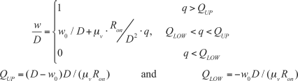
where w0 is the initial state for state variable w. The memristor state will move to a higher position, w > w0, if there is a positive charge injection. Likewise, negative charge injection will lower the memristor state; however, its state has a physical constraint: the state is bounded in between zero and total length D, namely 0 ≤ w ≤ D. Due to the physical constraint, the internal memristor state corresponds to the following effective Q range:
where QUP the upper limit of effective charge injection, and QLOW is the lower limit of effective charge injection. The expressions for them are listed as
The charge-controlled memristor state (length of doped region) can be described as
 [11.19]
where w0 is the initial state, D is the memristor length, μv is the average ion mobility and q is injected charges.
When actual charge injection goes beyond the upper limit of effective charge injection (QUP), the state will go no further after it reaches w = D. Likewise, the lowest state is at zero, even if charge injection goes lower than the lower limit of effective charge injection (QLOW). In the linear drift model, the memristor state will not go beyond total length D or go below zero. The state will be trapped at the boundary if injected charge is not within the effective Q range.
Equation 11.19 determines the charge-controlled memristance as
As Eq. 11.20 indicates, the resistance becomes charge dependent. Equivalently
where q is valid in the effective Q range. As a special case where w0 = 0 and Ron is small enough such that (Roff − Ron) ≈ Roff, charge-controlled memristance can be simplified to
Since the charge is integral of the current with respect to time, the state change is only functional of the integrated charge regardless of the current waveform.
Internal state w always comes back to the initial place, if the integral of current is zero over a certain time period. Figure 11.4 gives a brief demonstration taken from Ho et al. (2011). In Fig. 11.4(a), the current source Iin is composed of a positive pulse (t0 to t1) followed by a negative pulse (t1 to t2) with equal amplitude and width. In Fig. 11.4(b), starting from initial state w0 at t0, the state rises from t0 to t1 due to the positive pulse, causing the state rests at w1. Based on Eq. 11.16, the value for w1 is
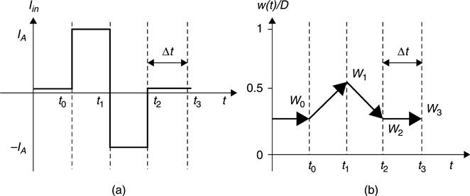
where (IA · Δt) is the charge injection by the positive pulse. From t1 to t2, the negative pulse follows, which moves the state from w1 to w2, and w2 can be expressed in terms of w1 as
where (−IA · Δt) is the charge injected by the negative pulse. The state w2 can be rewritten in terms of w0 by substituting Eq. 11.23 into Eq. 11.24, which gives w2 = w0. This shows that the final state w2 is the same as initial state w0. The type of input waveforms in Fig. 11.4(a) are referred to as zero net-charge injection inputs, because the integral of the current over the corresponding time period is zero. Zero net-charge injection waveforms can be any waveforms, as long as the integral over a period is zero, and it can bring the state back to the original level regardless of the initial state. However, the state comes back only when the charge exerted on to memristor is within the effective q range. Otherwise, the state will not return to the initial state level.
B Voltage-controlled memristance
If a memristor is flux-controlled, the state of memristor is controlled by the flux across the cell. Figure 11.5 shows a memristor biased by a voltage source Vin, and Vin, can be any waveform. Denote β the off/on ratio (Roff = Ron β). Equation 11.9 can be rewritten as

After certain manipulations using differential calculus, it becomes
where
and ϕ is the flux which is the integration of the voltage across the memristor. The solution to Eq. 11.26 would be
 [11.28]
where w(t = 0) = w0 is the initial condition. Note that Eq. 11.28 clearly indicates that w(t) is a function of the flux applied; it is indirectly dependent on the voltage across the memristor. The input voltage waveform with the same net flux injection leads to the same memristor state change. As a result, the flux-controlled memristor state can be described as
 [11.29]
where
 [11.30]
and
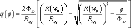
Due to the finite length D of the thin film, the internal memristor state is constrained as 0 ≤ w(t)/D ≤ 1, which corresponds to the following effective φ range:
Memristor state, w, would not be more than D when the applied flux across the memristor is over the effective upper bound (ΦUP), and it would not be lower than zero when the applied flux is smaller than the effective lower bound (Φ LOW). In other words, if the applied flux is larger than the upper limit of the effective range, φ would be the upper limit of effective injection. Likewise, φ would be the lower limit of effective injection, if the applied flux is lower than the effective range.
As Eq. 11.29 indicates, the memristance works as a flux driven resistance, thus it implies that
and the flux-controlled memristance can be written as
 [11.34]
The flux-control memristance, as indicated in Eq 11.34, is bounded between Ron and Roff.
There is a relation between charge-controlled and flux-controlled memristance, since flux and charge injection both can change memristor state. The memristance change by charge or by flux should be identical for the same memristor state change, thus
Therefore, the q–φ relationship can be expressed as
 [11.36]
According to the definition of memductance from Eq. 11.2, the memductance is
 [11.37]
Based on Eq. 11.5, the inverse of memductance gives memristance. Since memductance has flux as the control variable, the inverse of that gives flux-controlled memristance, which is the same as in Eq. 11.34.
Similar to the charge-controlled scenario, the memristor state change is also a function of the voltage integration, regardless of the waveform shape of the bias voltage. The change to the memristor states would be the same, as long as the flux injections (integration of their voltages) remain the same. In addition, a zero net-flux injection input, one whose integrated voltage over the time is zero, pushes the state of the memristor back to the initial level if the flux exerted on to the memristor is within the effective φ range, as in Eq. 11.32.
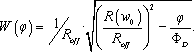
By utilizing Eqs 11.33 and 11.34, the applied flux needed across the memristor to move the state of memristor from an initial state w0 to an arbitrary state w is
If the applied voltage is a square-wave pulse with amplitude VA and width Tw, the flux across the memristor is described as
The time it takes to move the state of memristor from w0 to w can be derived. The input voltage magnitude is VA when time is between zero and Tw, and flux is accumulating in this time range. When time goes beyond Tw, the voltage magnitude is zero, so there is no more flux increment beyond time Tw. Hence, the total flux injection for a square-wave pulse is VA · Tw,,which is the amplitude times the width. The total flux injection determines the change of memristor state. With a given pulse magnitude VA, the required width needed to move memristor state from w0 to w is
As a special case, the required time needed to move the memristor state from w = 0 to w = D is the same as to move from w = D to w = 0, and the expression is
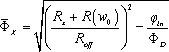
Furthermore, conisder a constant resistor Rx and a memristor connected in series and biased using a voltage source, as shown in Fig. 11.6. The voltage at node x is proved to be
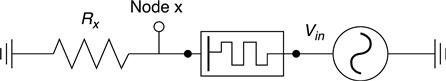
To prove Eq. 11.42, the input-output relationship of the divider circuit will be derived by solving φx in terms of φin analytically. Note that φin is the input flux injection, φx is the flux accumulated at node x, and φin − φx is the flux across memristor, M. Based on Kirchhoff’s Current Law (KCL), the KCL equation at node x implies that all the net charges into node x would be zero. Hence, the charges (integral of current) that went through the memristor, qx, should be the same as the charges that went through the resistor, so qx = φx/Rx. Accordingly, the flux across the memristor is φin − φx, and replacing φ by φin − φx and q by qx in Eq. 11.36 yields the charges that went through the memristor:
 [11.43]
in which φx has an unique solution of
 [11.44]
Since voltage Vx is the total derivate of φx, Vx is derived as
 [11.45]
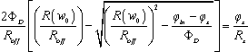
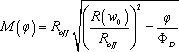
To verify that Eq. 11.45 is indeed the same as Eq. 11.42, we evaluate memristance M(φin − φx) by using Eqs 11.44 and 11.34. The result yields
where
 [11.47]
Finally, substituting Eq. 11.46 backing to Eq. 11.42 shows that it is exactly equal to Eq. 11.45. Therefore, the memristor series-connect resistor circuit in Fig. 11.6 indeed behaves as a voltage divider.
Moreover, the expression for the required input flux to move the memristor state from an initial to w for the divider circuit shown in Fig. 11.6 is
Equation 11.48 is derived from Eq. 11.38. The φ in Eq. 11.38 is the flux across the memristor. The φ would be φ = φin − φx for the case of a memristor series connected to a resistor. Since φx is already derived in Eq. 11.44, substituting φ = φin − φx into Eq. 1.38 yields Eq. 11.48. For a square-wave voltage supply, the time to move the state of memristor from w0 to w with a given amplitude VA is
As a special case, to move the state from w0 = 0 to w = D requires the same Tw as that needed to move from state w = 0 to w = D, and the Tw expression is
Furthermore, a memristor has an effective flux restriction due to finite length D. Equation 11.32 shows the effective φ range for a single memristor case. Similarly, the case of a memristor resistor connected in series would also have an effective range. The effective range for φin across both memristor and resistor is
where φin is integral of Vin and
Finally, a zero net-flux input voltage pattern will insure that the state of the memristor comes back to the initial position for the circuit shown in Fig. 11.6. This property, where the state comes back to initial position, holds true for both a single memristor cell and a memristor series connected with a resistor cases. This contributes important design guidance for ensuring read stability, as discussed in detail in later sections. To prove this, simply set φin equal to zero in Eq. 11.48 and solve possible solutions for R(w); two possible solutions exist: one is w = w0, and the other is outside of the memristor physical range. Therefore, the state will be back to the initial level as w = w0. However, this is true only when the effective flux range condition as in Eq. 11.51 is satisfied.
A brief summary on the above-mentioned memristor characteristics are listed into 14 properties in the Appendix at the end of this chapter.
Memristor device characteristics in the nonlinear drift model
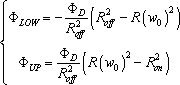
In the nonlinear drift model, the above-mentioned window function in Eq. 11.10 reflects the following fact: as the memristor state moves toward the boundary (w = 0 or w = D), the dopant drift velocity drastically decreases. However, the state equation behaves close to the linear drift assumption in the region between, in which the properties in the linear drift model are preserved. As shown in Fig. 11.7, the linear drift operation region is 0.1 < w < 0.9. Accordingly, it is desirable to operate in a smaller linear range, say W0 ≤ w ≤ W1, for faster switches and easier design. When approaching the boundaries, the constant average mobility used in the linear model, μv, is the upper bound of the nonlinear average mobility used in the nonlinear models.
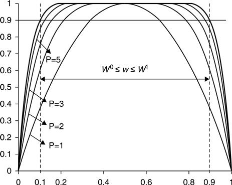
11.3.2 Logic regions of operation
For simplicity, a memristor is at logic zero when 0 < w/D < 0.5 and logic one when 0.5 < w/D < 1.0. The corresponding ideal output low and high levels are w/D = 0 and w/D = 1.0, respectively. To account for possible noise injections, a safety margin is specified for each logic output: 0 ≤ w/D ≤ OL, (OL = WL/D < 0.5) for logic zero, and OH ≤ w/D ≤ 1.0 (OH = WH/D > 0.5) for logic one. The region in between OL ≤ w/D ≤ OH is an unsafe region that should be avoided for read/write data integrity. Figure 11.8(a) illustrates the situation where OL = 0.4 and OH = 0.6.
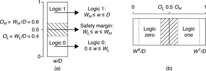
On the other hand, the logic zero/one region needs to be defined before the memristor cell is used as memory. When considering the boundary effect, the memristor state is to keep off the boundary. Moreover, W0 and W1 are the lines seperating the nonlinear region and the linear region. Figure 11.8(b) shows an illustration of the defined output levels.
11.3.3 Read/write operations of memristor-based memory
Write operation scheme
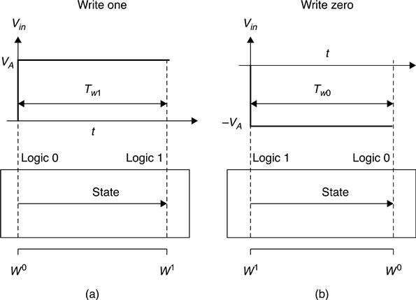
To write a logic value to a memristor cell, the proposed way is to have the structure as in Fig. 11.5, where the memristor state will be altered by the flux injection. Let the applied voltage be a simple square-wave pulse with amplitude VA and width Tw.
Assume initially the state w0 is w0 = 0, and it is desired to write logic one to the cell. For the write process, input voltage Vin generates a square-wave pulse that has magnitude + VA and width Tw1 (Fig. 11.9(a)). Pulse width Tw1 must be longer than the minimum required time TOHw1 to insure the state rests inside the logic one region after write. The minimum required time TOHw1 is
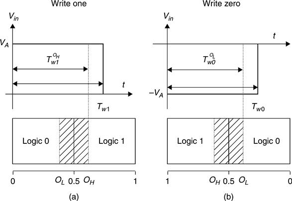
where WH is the boundary for logic one region, which can be set arbitrarily. If the initial state w0 is not at w0 = 0, but somewhere inside the logic zero region, a successful write can be guaranteed as long as ![]() . Similarly, to write a logic zero, the input voltage Vin is a negative square-wave pulse (− VA) with duration Tw0 (Fig. 11.9(b)). The minimum required time TOLw0 would be
. Similarly, to write a logic zero, the input voltage Vin is a negative square-wave pulse (− VA) with duration Tw0 (Fig. 11.9(b)). The minimum required time TOLw0 would be
where WL is the boundary for logic zero region. The write zero process would be successful if pulse width Tw0 is at least greater than TOLw0. Thus, a write signal that has duration equal or larger than the derived minimum required time insures a successful write.
Moreover, the memristor state w = 0 and w = D are as ideal logic zero and logic one states in linear drift model. Equation 11.41 specifies the required pulse widths to move a state from w0 = 0 to w = D or move from w0 = D to w = 0. Suppose the memristor behavior follows the nonlinear drift model. It is very difficult to move the memristor to the boundary (w = 0 and w = D), because of the low ionic drift velocity near the cell boundary. Therefore, it is better to set arbitrary states W0 and W1 to be the ideal logic zero and one state and avoid the boundary. The goal of write operation is to precisely move the state to W0 for logic zero and W1 for logic one. The proposed write scheme is shown in Fig. 11.10, and Fig. 11.11 illustrates the corresponding pulses for write one/zero process.

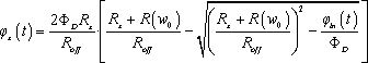
Suppose the write one process is performed. The positive input voltage magnitude VA raises the state (Fig. 11.11(a)), and the rising of the state will increase the voltage at node x (Vx). By using the voltage divider property derived before, Vx can be expressed as
The write one process is terminateded when Vx reaches the reference voltage VW1ref The reference signal to write to desire logic one state is designed to be
where W1 is the ideal logic one state. When Vx reaches the reference signal in Eq. 11.57, the memristor state reaches the desire-one state, and a feedback signal is sent to switch off the write pulse.
Similar to the write zero operation, a constant magnitude −VA is applied to the memristor cell resulting in lowering of the memristor state. The reference voltage is set according to the equation below for the write zero process:
In summary, the write process sets Vin to a constant VA, or −VA magnitude pulse depends on whether writing is logic one or zero, and the reference signal is set accordingly.
Read operation scheme
The proposed memristor-based read cell structure is shown in Fig.11.12; such a read scheme works for both linear and nonlinear models. A read process is composed of two stages, convert stage and amplifier stage. In the convert stage, the memristor state information converts into a voltage signal, Vx, which reflects the memristor state information. The sense amplifier stage determines the logic based on Vx and output full-swing digital scale.
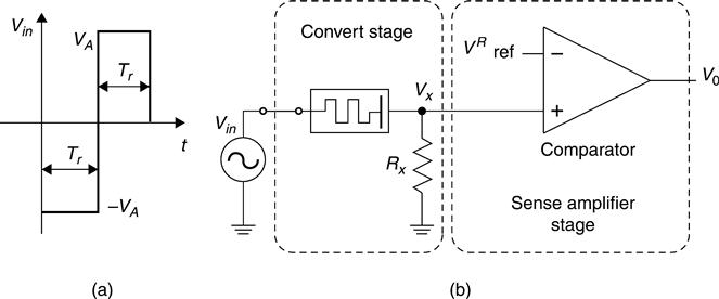
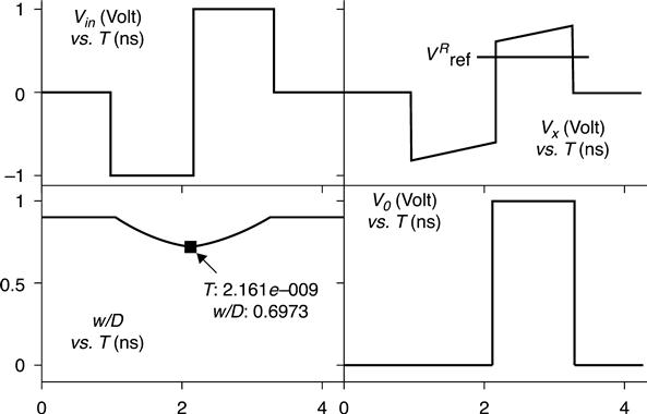
The designed read signal pattern has a negative pulse followed by a positive pulse, with equal magnitude and duration (Fig. 11.12(a)). This read pattern will enforce zero net flux injection over one period to avoid altering the memristor state after a read access. Based on the memristor property mentioned in Section 11.3.1, the zero net flux injection read pattern avoids altering the memristor state after read cycles. The first negative pulse cycle decreases the state and the follow-up positive cycle bring the state back up.
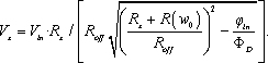
The resistor Rx, in series with the memristor shown in Fig. 11.12(b), is to convert the memristor state information into a voltage signal form, since the current through the memristor carries the memristor state information. Thus, the voltage at node x(Vx) reflects the memristor state. Let the reference voltage set to
where VA is the pulse magnitude shown in Fig. 11.12(a). During the first read cycle, the negative pulse produced makes Vx negative. That would make Vo low because Vx will be less than the reference voltage regardless of the memristor state. At the second cycle of read pattern, Vx is compared with VRref to determine the logic. If the state is below half of D, Vx will be below VRref, and logic zero is read. Similarly, Vx higher than VRref indicates the memristor state is in the upper half of its length D, and logic one is read. For that, the corresponding Rx is
This way, the second half of the read cycle can distinguish logic zero and logic one, and the device should read the output on the second half cycle to retrieve the stored data.
Figures 11.13 and 11.14 are the simulation results taken from Huang et al. (2010) and illustrate the read operation. When the memristor state is initially at logic zero, the input negative pulse (first-half cycle) will decrease the memristor state and the coming positive pulse (second-half cycle) increases the state. As shown in Fig. 11.13, since the read signal has a zero net flux injection pattern, the state is back to the initial level after read. Because the state remains under half of D for the whole time, the memristor cell has a high resistance value. Due to this high resistance, the magnitude of Vx remains lower than VRref throughout the read operation period, thus logic zero is successfully read. Similar to the logic one case illustrated in Fig. 11.14, the state travels within the logic one region as designed due to the zero net-flux injection input pattern. Since the memristance is low in the logic one region, the magnitude of Vx is high. The output Vo rises high in the second-half of read cycle, since Vx is higher than the reference voltage during that period. Therefore, the detector should read the second half of the cycle, since it reflects the correct logic state stored in the memristor.

11.4 Other promising memristor applications
11.4.1 Memristor-based implication logic
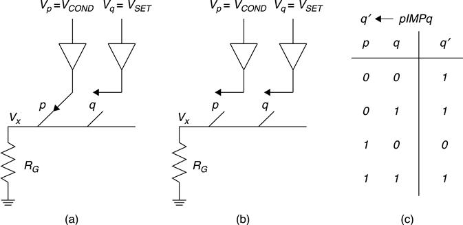
Recently, scientists have demonstrated that memristor cells can be used for logic operations. The research group at HP (Borghetti et al. 2010) shows that the hysteretic resistor crossbar array can execute material implication (IMP) logic (they are also referred to as ‘stateful’ logic). The IMP logic is a fundamental Boolean logic operation. The notation for IMP logic operating in two state-variables p and q is denoted by (pIMPq). The (pIMPq) operation is equivalent to the Boolean logic of (NOT p) OR q. The execution for (pIMPq) logic requires some time to perform broken logic, and the result will be written back to the q state. Let q’ be the final state of variable q. The notation q’ ← (pIMPq) means the result of (pIMPq) stores to the q variable.
According to Borghetti et al. (2010), the memristor cell is treated as a simple switch; a closed switch represents logic one, and an opened switch represents logic zero. Control of the input magnitude is able to open, close or unchange the state of switch. The terminology used is:
• VSET: a ‘strong’ negative magnitude input pulse can close the switch;
• VCLEAR: a ‘strong’ positive magnitude input pulse can open the switch;
• VCOND: a ‘weak’ negative magnitude input pulse does not change the state of the switch.
If VSET or VCLEAR is applied at the input of a particular branch, it will unconditionally close or open that particular switch. If VCOND is applied, the voltage VCOND is able to go to node x (Vx) when the switch is closed. Otherwise VCOND cannot pass through if the switch is opened. Figure 11.15(a) gives an example demonstrating the (pIMPq) logic. The p switch is initially closed (logic one) and the q switch is opened (logic zero). The voltage at node x will be VCOND, since the p switch is closed. This makes the voltage across the q memristor to be VSET minus VCOND, and the q switch remains opened because VSET-VCOND is a ‘weak’ negative magnitude voltage. In Fig. 11.15(b), supposing p and q switches are both originally stored zero, the voltage VCOND cannot pass through p switch. When VSET is applied a q switch branch will close the q switch, since VSET is a ‘strong’ negative magnitude pulse to close the switch. The complete truth table for IMP logic is shown in Fig. 11.15(c).
Furthermore, Borghetti et al. (2010) and Kvatinsky and Kolodny (2011) demonstrated Boolean NAND logic function using three memristors. In Fig. 11.16(a), the memristors p and q are acting as the input, with the result being stored to memristor s at the end. Figure 11.16(b) illustrates the three steps to perform a NAND operation. In STEP 1, the VCLEAR signal is given to unconditionally open the s switch. Next, material implication logic will be performed on the p and s switches, and the result, denoted by s′, is stored to s switch after (pIMPs) is completed. There are only two possible combinations in STEP 2, since the s switch is forced to have logic zero: either (p = 0 and s = 0) or (p = 1 and s = 0). In STEP 3, the material implication logic on q and s′ is performed, and the result is denoted as s″. As shown in Fig. 11.16(c), the outcome of the three sequences is equivalent to the truth table of a NAND operation.

In conclusion, the memristor produces ‘stateful’ logic operations for which the memristive devices function as logic gates that use resistance rather than charge or voltage as a physical state variable. Thus, it saves computational power in this sense. However, such an operation requires consecutive steps. Timing is an issue for today’s memristor when competing with modern CMOS technology.
11.4.2 Neuromorphic and biological systems
Neuromorphic circuits received much attention after the memristor device came out. Recently, there are two types of neuromorphic circuits: the learning circuits and neural networks (Pershin et al. 2010). More specifically, learning circuits are the circuits that can demonstrate self-adaptation or smart operation, and neural network circuits are built based on biological structures and meant to mimic the learning functionalities from a biological aspect. The neuromorphic circuit is a large area of research, in part because a large part of the analog science detail has to do with advances in cognitive psychology, artificial intelligence modeling, machine learning and recent neurology advances. In fact, scientists and engineers have already started the work on neural field in the past decade. The earliest work traces back to 1960, which is the ADALINE neural network (Widrow et al. 1961). The research was halted due to difficulties on implementing the large size of complex circuitry on a chip. Due to the advance of nanotechnology in the 20th century, such a task became feasible. Moreover, scientist has shown that the memristor device follows the behavior of the synapse (Jo et al. 2010). Thus, the memristor has made it possible to implement a neural network on to a chip. In short, many scientists and researchers are exploring innovative approaches that enable revolutionary advances in devices for memristor-based learning circuitry and neural-synaptic mimicking.
11.5 Acknowledgement
This material is based on work supported by the National Science Foundation under Grant No. 0917204.
11.7 Appendix: Memristor characteristic properties
Property 2: The state (length of the doped region) is charge-controlled and can be described as

where w0 is the initial state, D is the memristor length, μv is the average ion mobility and q is injected charges. QUP is the upper limit of effective charge injection, and QLOW is the lower limit of effective charge injection.
Property 3: Charge-controlled memristance can be described as
The equation is valid in the range: QLOW ≤ q ≤ QUP
Property 6: The state (length of the doped region) is flux-controlled and can be described as
where β denoted the off/on ration (Roff = Ron β), w0 is the initial state, D is the is the memristor length, μv is the average ion mobility and φ is injected flux. ΦUP is the upper limit of effective flux injection; ΦLOW is the lower limit of effective flux injection, and ![]()
Property 7: Flux-controlled memristance can be described as
The equation is valid in the flux range: ΦLOW ≤ φ ≤ ΦUP
Property 10: The memristor state is initially at w0. Suppose the state of memristor is desired to move to a feasible state w by a square-wave voltage pulse that has amplitude VA and width Tw, then the required width Tw is
Corollary 10.1: Suppose a voltage square-wave pulse with amplitude VA and width Tw is applied to a memristor. The duration needed for the memristor state to move from w = 0 to w = D is the same as that required to move the state from w = D to w = 0, and the required duration Tw is
Property 11: In the voltage divider shown in Fig. 11.6, the node voltage response at node x is given by
where Vx is the voltage at node x, φin is the flux injection, φx is the flux accumulated at node x and φin − φx is the flux across memristor M.
Property 12: For the circuit in Fig. 11.6, assume the voltage source Vin is a square-wave pulse with an amplitude VA and a width Tw. To move the state of the memristor from w0 to w, the required width Tw is
Corollary 12.1: For the circuit in Fig. 11.6, assume the voltage source V in is a square-wave pulse with an amplitude VA and a width Tw. The duration needed for the memristor state to move from w = 0 to w = D is the same as that required to move the state from w = D to w = 0, and the required duration Tw is
Property 13: When a memristor is connected in series with a resistor (Fig. 11.6), the effective range for φin across both memristor and resistor is
where φin is integral of Vin and
