Overview of non-volatile memory technology: markets, technologies and trends
R. Bez and A. Pirovano, Micron, Italy
Abstract:
In the last decade, the impressive growth of the portable systems market has attracted the interest of the semiconductor industry in non-volatile memory (NVM) technologies for both code and mass storage applications. The current NVM mainstream is based on Flash technology and it is expected that NOR and NAND Flash will be the high volume NVM production for several years. There is industrial interest in alternative technologies that exploit new materials and concepts to go beyond Flash technology, to allow better scaling and to enlarge memory performance. We review the current status of charge-storage based Flash memory technology and introduce the most promising alternative memory concepts. Expected trends and future perspectives are also discussed.
Key words
Flash memories; emerging memories; FeRAM; MRAM; resistive memories; phase-change memories
1.1 Introduction
The explosive growth in the market for mobile phones and other portable electronic devices has been propelled by ongoing decreases in the cost and power consumption of integrated circuits. This is particularly true for non-volatile memories (NVM) based on floating-gate technology, also known as Flash memory. The current mainstream of NVM technology, based on floating-gate Flash technology, is expected to be the reference technology for the next years. Nevertheless, Flash memories have technological and physical constraints that make their further scaling more difficult. In this context there is industrial interest in alternative NVM technologies that exploit new materials and novel concepts to go beyond Flash technology, to allow better scaling and to enlarge memory performance.
In Section 1.2, a brief overview of the NVM memory market will provide some insights in the actual trends, showing that opportunities still exist for novel memory concepts that can provide a competitive advantage. In Section 1.3, the mainstream NVM technology, namely Flash memories, will be reviewed, explaining the working principle of the floating gate concept and highlighting the differences among the existing implementations of such concept in real products. Scaling trends and limitations of Flash technology will also be discussed, thus introducing Section 1.4 on novel NVM concepts that are today under development and that aim to become major players in the NVM market. Section 1.5 is dedicated to the most advanced concepts under development to provide alternative solutions for the storage memory market, with solutions that try to move towards threedimensional (3D) integration. Finally, Section 1.6 will provide some guidelines to the reader that can help in the understanding of actual NVM trends and the evolution of memory technologies.
1.2 The non-volatile memory (NVM) market and applications
The dramatic growth of the NVM market started in 1995 and has been fuelled has been fuelled by two major events: the introduction of Flash memories1–3 and the and the development of battery-supplied electronic appliances, mainly mobile phones. Almost all electronic systems require the storage of some information in a permanent way. The most typical application for NVMs has traditionally been program codes for microcontrollers, parameters for DSPs, boot systems with other types of mass storage media, data and parameters for security codes, trimming of analog functions, end- user programmable data, system self- diagnostic, etc.4 Traditionally, NOR-Flash technology was the most suitable for code-storage applications, due to the low access read time requested for the eXecution-In-Place (XiP) of the stored code. Starting from the first years of the new millennium, a novel trend in the NVM market appeared in conjunction with widespread new data-centered applications such as PDAs, MP3 players and digital still cameras. In these portable devices, a huge role is played by the available size of the NVM devices, in order to store the data at the lowest possible cost. In this scenario, NAND-Flash technology entered the market and rapidly became the mainstream technology, even surpassing DRAM in the role of technology driver.
Although the very low cost was the primary driver for the exponential growth of NAND Flash technology, in the last few years such devices have been able to demonstrate an edge over other technologies in terms of performance for handling large amounts of data. These capabilities combined with the continuously reducing costs per GigaByte (GB) recently created a new market opportunity for Flash technology in data-storage application as magnetic Hard Disk Drive (HDD) replacement. NAND-Flash based HDDs, also called Solid-State Drives (SSDs), are now available with densities of up to 512 GB at a very reasonable cost, and provide much better performance than HDD in terms of sustained throughput, access time, instant-on capabilities and ruggedness. However, considering the still existing difference in terms of cost per GB of an SSD device with respect to a magnetic HDD (almost an order of magnitude), a complete replacement of HDD is not yet feasible and a new scenario is going to appear on the computing platform. In fact, the usual hierarchy of memories used to manage data manipulation and storage is refined with the introduction of novel ‘memory layers’ that are intended to mitigate the weaknesses of traditional memory systems (i.e. costs and power consumption for DRAM, slowness for magnetic HDD).
A very interesting opportunity has been identified for a memory system that could stay in-between DRAM and HDD, both in term of latency and costs (Fig. 1.1). Such a memory system, conventionally defined as Storage-Class Memory (SCM), represents the ideal realm for NVM technologies due to their low-power capabilities.5 However, stringent requirements in term of speed and costs must also be met. Considering today’s specifications, NAND-Flash based SSD could fit the SCM definition and fulfill SCM requirements in the region close to HDD. However, today’s performances of Flash technology are not enough to fill the gap towards DRAM, in particular in terms of speed and endurance, and market opportunities exist for novel NVM technologies capable of meeting such requirements. Among the proposed emerging technologies, Phase-Change Memories (PCM) is the only alternative technology available today in large volume production.6 Although their usage is still limited to specific applications in wireless systems, some attempts already demonstrate their capability to provide much better performance than Flash-NAND based SSD,7 thus fostering this technology as a major player for filling the gap between the existing data storage solutions and DRAM.

1.3 Developments in charge storage memory technology
For more than 40 years, all programmable non-volatile semiconductor memory technologies have been based on the ‘floating-gate’ concept. This basic concept dates back to 1967, when Frohman-Bentchkovsky first presented it. Later it evolved into different technologies, such as EPROM, EEPROM, and finally Flash.8,9
1.3.1 Floating gate concept
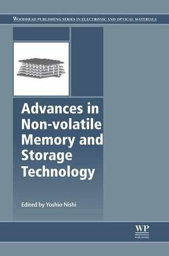
A floating-gate memory cell is basically an MOS transistor with a gate completely surrounded by dielectrics (Fig. 1.2), the floating-gate (FG), and electrically governed by a capacitive-coupled control-gate (CG). Being electrically isolated, the FG acts as the storing electrode for the cell device. Charge injected into the FG is maintained there, allowing modulation of the ‘apparent’ threshold voltage (i.e. VT seen from the CG) of the cell transistor. Obviously the quality of the dielectrics guarantees the non-volatility, while the thickness allows the possibility to program or erase the cell by electrical pulses. Usually the gate dielectric, i.e. the one between the transistor channel and the FG, is an oxide in the range of 9 to 10 nm and is called the tunnel oxide, since Fowler-Nordheim (FN) electron tunneling occurs through it. The dielectric that separates the FG from the CG is formed by a triple layer of oxide-nitride-oxide (ONO). The ONO thickness is in the range of 15 to 20 nm of equivalent oxide thickness. The ONO layer, as an interpoly dielectric, has been introduced to improve tunnel oxide quality. In fact, the use of thermal oxide over polysilicon implies a growth temperature higher than 1100 °C, impacting the underneath tunnel oxide. High temperature post-annealing is known to damage thin oxide quality.
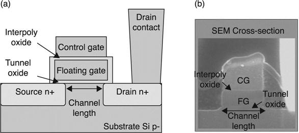
If the tunnel oxide and the ONO behave as ideal dielectrics, then it is possible to schematically represent the energy band diagram of the FG MOS transistor (Fig. 1.3). It can be seen that the FG acts as a potential well for the charge. Once the charge is in the FG, the tunnel and ONO dielectrics form potential barriers. The neutral (or positive charged) state is associated with the logical state ‘1’, while the negative charged state, corresponding to electrons stored in the FG, is associated with the logical state ‘0’.
Until the introduction of Flash memory, there were two different categories of electrically programmable floating-gate non-volatile memories: the EPROM (Electrically Programmable ROM) and the EEPROM (Electrically Erasable and Programmable ROM). EPROM is a one-transistor memory cell and therefore can provide high density and cost effectiveness, but can only be erased by exposure to UV light. Mounted in very expensive ceramic packaging with a transparent window, EPROMs were used for system debugging, to be substituted in volume production by either masked ROM or OTP (One Time Programmable) EPROM, i.e. the same EPROM devices in more cost-effective plastic packages. EEPROMs feature electrical erase capability, with fine granularity (even single byte) and good endurance (over one million program/erase cycles). However, because of the complex structure of their memory cell, EEPROM are expensive and their cell size cannot be scaled in proportion to the lithography features. As a consequence of their different cost/performance trade-offs, EPROMS have been mostly used for code storage, while EEPROM have been used to store parameters and user’s data.
Offering electrical erase capability, traditionally featured by the expensive EEPROM, at cost and density comparable to EPROM, Flash memories have not only taken a large portion of their progenitor’s markets, but have also greatly expanded the field of application of non-volatile memories. This impressive growth has also been associated with the development of personal portable sets. Systems such as PDAs and mobile phones cannot use magnetic disks because of size and power consumption. Therefore, in these systems, besides the usual requirements for non-volatile storage of codes and parameters, there is a demand for mass storage (operating system, application programs and user’s files) that must be covered by semiconductor memories. Moreover, the development of multimedia applications and the convergence of personal consumer appliances towards portable systems that manage data, communication, images and music, is dramatically increasing the demand for a friendly way of storing and moving large files: memory cards, in different formats, and USB keys are the rising segments that are further fuelling the growth of the Flash memory market. All these applications are making the fortune of Flash memories and are creating a huge opportunity for the emerging memory concepts that promise to out-perform them.
Among the many different Flash technologies that have been conceived and the less that have reached the maturity of volume production, two dominant ones can be identified as:
1. NOR Flash: the mainstream technology for the applications that require the storage of codes and parameters, and more generally for embedded memories (system-embedded and chip-embedded) that has to provide random memory access;
2. NAND Flash: only provide serial access but higher density and lower cost than NOR, and are therefore the dominant technology for data storage and memory cards.
1.3.2 NOR Flash technology
All the nice features of NOR Flash products are inherently related to the memory cell concept and the memory array organization. The cell is a one-transistor cell made of a stacked-double-poly floating-gate MOS device (Fig. 1.2), which is programmed by channel-hot-electron (CHE) injection and erased by Fowler-Nordheim tunneling. The memory cells are arranged in a NOR type array organization, which means that all the cells are connected parallel to a common ground node and the bit lines are directly connected to the drain contacts of memory cells.
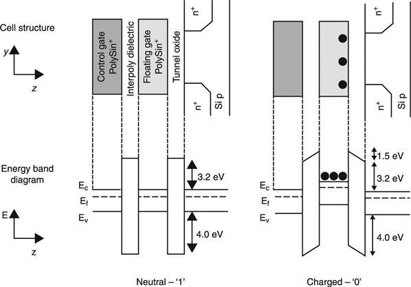
Figure 1.4 shows the two schematic cross-sections of the cell, along the y-direction (bit line) and the x-direction (word line). The cell area is given by the x-pitch times the y-pitch. The x-pitch is given by the active area width and space, considering also that the FG must overlap the oxide field. The y-pitch is constituted by the cell gate length, the contact-to-gate distance, half contact and half source-line. It is evident that both contact and source-line are shared between two adjacent cells (Fig. 1.4).
If space applications and related cosmic ray effects are excluded, charge storing in a floating gate is the most reliable mechanism employed in programmable memory technology as far as data retention; due to the very high (3.2 eV) energy barrier that electrons have to overtake to escape from the floating gate. The channel-hot-electron programming mechanism is the best for immunity to program disturbances and does not require scaling tunnel oxide to reduce the memory cell channel length, allowing preservation of good data retention while scaling cell size. The NOR array organization is best for high speed and noise immunity. The combination of NOR array and CHE programming makes this technology the most suitable for multilevel storage, which helps to boost the density for very cost sensitive applications. Last but not least, this cell concept has proved to be well compatible with advanced logic processes and is widely used for embedded memory in system-on-a-chip (SOC).
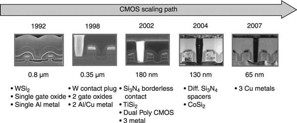
The NOR Flash technology evolution has followed standard CMOS (complementary metal-oxide semiconductor), introducing into the basic process flow many of the materials and modules already developed.10 In particular, considering the requirements for fast random access time, the supply voltage for mobile application down to 1.8 V, and the efficient programming and erasing algorithm execution, starting from the 180 nm technology node, the CMOS structure has mainly followed the high performance logic roadmap.11–13 Figure 1.5 shows NOR Flash cross-sections for different generations, from 0.8 um to 65 nm. For every generation are highlighted the materials and the basic modules that have been introduced. It can be observed that there are two key elements that have evolved: in the front-end the gate material, from WSi2 to the CoSi2 and in the back-end the metallization, from single aluminium to three copper layers. The number of metal interconnections still represent a large difference with respect to the most advanced logic processes. In fact, while state-of-the-art microprocessor processes back-end features of more than six layers of metals, in the Flash memory, considering both the performances and the cost constraints, only three-four metal layers are used.
1.3.3 NAND Flash technology
NAND Flash memory was born in the mid-1980s,14 just after the presentation of the NOR cell, but it took longer to become a mainstream memory and to find the right application, which today is for semiconductor mass storage. NAND Flash has basically the same memory cell structure as NOR, but has a totally different array organization (Fig. 1.6) and employs a different programming mechanism.

The memory array is organized in NAND strings; i.e. a number of cells, usually 16 or 32, are connected in series between ground and the bit-line contact. This organization increases the density vs NOR, which instead requires a ground line and a bit line contacted to every two cells, but dramatically affects speed. In fact, every cell must be read through a number of other cells (15 or 31), strongly reducing the read current, which results in much longer access time (microseconds compared with the tens of nanoseconds of NOR Flash) and practically prevents usage of this technology for random access memories, thus restricting it to serial non-volatile memories only.
The programming mechanism utilized by NAND Flash is Fowler-Nordheim tunneling. The programming time using the FN tunneling is per se longer than that using the channel hot electron (~300 us for FN and ~1 us for CHE), since it must work in the electric field regime across the tunnel oxide that guarantees the necessary reliability requirements. On the other hand, being a programming mechanism that requires very low current, FN tunneling allows a very high on-chip parallelism for programming and, as a consequence, a very high writing throughput, which is a key feature for mass storage. The very high density and the high programming throughput make NAND the dominant technology for mass storage.
In terms of process architecture, the NAND Flash is different from the NOR Flash. The cell architecture is common: same Floating Gate concept, same one-transistor stacked-gate cell. However, the difference is in the CMOS transistor architecture. In NOR, the logic is designed to be high performance in order to speed the program/erase algorithm and to gain the fastest random access time. However, NAND transistors are designed to be as far as possible compatible with the cell structure, to minimize the mask number and then to reduce the process cost.
1.3.4 Flash memory scaling
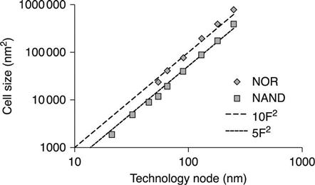
The scaling of Flash technology has been straightforward for the last 20 years (Fig. 1.7). A rough comparison of NOR and NAND Flash characteristics shows that one of the most important parameters that differentiate the two types is cell size.15 For many generations, in a NOR cell the size was 10 F2, where F is the technology node, while in the NAND cell the size was around 4.5 F2, giving rise to a NAND memory density higher than the NOR density. The different cell size comes from the array organization and from the cell layout. In a NOR cell, a contact is shared by every two cells, basically doubling the number of lithography features needed to define the cell. Moreover, the CHE programming does not allow an aggressive scaling of the cell gate channel length, which instead occurs in NAND, where the cell gate length and space define the technology node. The main physical limits that prevent further scaling of the cells are the cell-to-cell interference, due to the parasitic capacitive coupling among neighboring floating gates and low coupling ratio with the control gate, which also results in a small stored charge.16
The effective channel length scaling will be limited by the ability to further scale the tunnel oxide and the inter-gate oxide-nitride-oxide stack. Tunnel oxide thickness scaling is limited by intrinsic issues related to Flash cell reliability, in particular by charge retention, mainly after many writing cycles. Stress Induced Leakage Current (SILC)17–19 could give rise to a single bit failure with unbearable statistics, if the thickness is less than 9 nm. Only if ECC is used, as happens today in NAND Flash, the thickness can be scaled down to 6 to 7 nm. Obviously the ECC pays in terms of worst reading performances that do not impact the NAND memory specification. Further reduction of cell size will increase the requirements for error correction beyond the feasibility limits.
Despite the fact that the floating gate concept was predicted to face technological limits beyond the 32 nm technology node, NAND memory density has been shown to downscale to the 20 nm node with the multilevel cell concept applied.20 Such an achievement is partially due to the fact that for NAND products, a significant reliability drop (in particular for endurance) is acceptable, considering the large ECC available and the processing power of dedicated controller in SSD applications. A similar trade-off is unacceptable for NOR Flash application, thus making their scaling more challenging. NOR Flash has thus reached its scaling limitation at 45 nm, even considering the constant/declining market demand that is not fostering additional development efforts for this technology, while NAND is available at 20 nm and 16 nm technology is currently under development.
One of the most important attempts made in the last ten years, to mitigate scaling limitations while retaining the very high integration density of NAND Flash architecture, has been to tentatively replace the conventional floating gate with a charge trapping layer. Silicon nano-crystal trapping layers have been investigated in the past,21 but they present a few drawbacks, such as reduced threshold shift and the presence of percolation paths between source and drain, that become more severe with the scaling of the cell size. Silicon nano-crystal technology requires careful control of nano-dots size, dimension, shape and density, because these parameters significantly impact on the device performance and reliability. Moreover, the down-scaling of this technology is expected to be difficult beyond the 32 nm technology node, due to the minimum nano-crystal size so far achieved in a reproducible way.
Other alternatives include the use of a continuous trapping layer (charge trap memories, also called CT memories), such as silicon nitride in the SONOS device architecture.22 This approach should solve several of the scalability issues: the charge is trapped in a thin dielectric layer, and so there is no problem of capacitive interference among neighbouring cells; since the charge is stored in electrically insulated traps, the device is also immune to SILC, the parasitic leakage current caused by single defects in the dielectric layer, while in conventional floating gate devices, even a single defect can discharge the whole floating gate, which is a conductive storage medium. The replacement of the floating gate with a trapping layer reduces the overall thickness of the gate stack, and allows for easier integration of the cell in the CMOS process. In this architecture, the charge is trapped in a silicon nitride layer, inserted between two silicon oxide layers, which act as a tunnel dielectric and a blocking layer to prevent charge injection from the control gate.
Although this cell architecture has been known since the 1980s, and in spite of its better compatibility with standard CMOS process flow and lower costs, it has lost ground in favour of the floating gate architecture, because of several fundamental problems:
• Cell programming is limited by the erase saturation, which takes places because of parasitic electron injection from the control gate through the top oxide, balancing the hole injection from the substrate.
• The thinning of the tunnel oxide (< 2.5 nm) improves the threshold window and the programming speed, but results in poor retention, even at room temperature, because of direct tunnelling through the tunnel oxide, and charge mobility in the nitride layer.
• Increasing the tunnel thickness improves the retention, but requires larger programming voltages, reduces the speed and activates the tunnelling through the top oxide.
Despite the scaling issue of the floating gate concept, the actual drawbacks of the CT memories made the conventional planar Flash a preferred choice for mainstream technologies, thus limiting the usage of CT layers in mainstream Flash production.
1.4 Alternative memory storage concepts
To improve the performance and scalability of floating gate devices, innovative concepts for alternative NVM have been proposed in the past and are still under investigation today, to find the ideal memory that combines fast read, fast write, non-volatility, low-power, unlimited endurance and obviously at a cost comparable with Flash or DRAM. The main class of emerging NVM technologies so far investigated is based on inorganic materials and includes the alternative memory concept with the highest maturity level, namely Ferroelectric Memories (FeRAM), Magnetoresistive Memories (MRAM), Resistive RAM (ReRAM) and Phase Change Memories (PCM).
1.4.1 Ferroelectric memories
FeRAM is one of the few alternative NVMs that has been commercialized to date, even if at a technology node much more relaxed than the one used for Flash memories and with several challenging technological problems, mainly related to new materials and new manufacturing technologies. Two classes of ferroelectric materials are currently used for FeRAM memories: perovskite structures and layered structures. The perovskite material most used for ferroelectric memories is PbZrxTi1 -xO3 (PZT), while the layered ferroelectric choices for FeRAM memories are either strontium-bismuth-tantalate Sr1-yBi2 + xTa2O9 (SBT) or lanthanum substituted-bismuth-titanate Bi4-xLaxTi3O12 (BLT). Among them, the preferred option is represented by PZT, usually deposited with the MOCVD technique at temperatures higher than 600 °C.
Ferroelectric materials can be polarized spontaneously by an electric field. Polarization occurs as a lattice deformation of the cubic form below the Curie point, the temperature above which the material becomes paraelectric. For example, in PZT, the Ti atom can be moved by an electric field into two stable positions that are above and below the oxygen plane of the structure. Therefore, the most important properties of ferroelectric materials is their residual permanent polarization, which is in the range of 10 to 30 μC/cm2. The voltage required to switch the permanent polarization is in the range of 1.5 to 3 V for typical deposited layer thicknesses of 70 to 100 nm. It follows that ferroelectric memories can be a valuable solution for low-power and very low-voltage applications, such as battery operated embedded system, smartcard and RF ID applications.
One of the most challenging features of this technology is represented by the integration of the ferroelectric layer into a standard CMOS process. The bottom and top electrode of the ferroelectric layer must be realized with a specific alloy, usually constituted by Ir and Pt. Hydrogen contamination of the ferroelectric material must be avoided in order to prevent the reduction of the permanent polarization capability, thus requiring a specific barrier layer surrounding the ferroelectric capacitor. At the same time, oxygen can diffuse during the high temperature treatment required for ferroelectric alloy deposition, oxidizing the underlying metal layers. Finally, specific care must be devoted to the capacitor shape definition through dry etching, to the final dielectric layer used to seal the capacitor from the surrounding environment and to the effect of the plasma damage due to the CMOS back-end process, resulting in a possible discharge through the capacitor that destroys its data storage capabilities.
Endurance, also called electric fatigue, is the most important reliability characteristic and is related to a decrease in the ability to switch the memory cell into the opposite state, after remaining programmed in one state for long periods of time. This effect is related to the polarization shift in the hysteresis loop and is proportional to the increasing number of switching cycles. Nevertheless, the write cycle (but also the read cycle, since several proposed cell structures have a destructive reading) is expected to have an endurance level of about 1012, which will suffice for a wide majority of high-demanding storage applications. To date, several FeRAM cell structures have been proposed, with the ferroelectric material integrated either into a separate storage element, i.e. a ferroelectric capacitor,23 or into the selection element, i.e. a ferroelectric FET transistor. 24 In the latter case, the storage and the selection elements are merged.
The first cell type can be used in both the two-transistor/two-capacitor (2 T/2C) cell and the one-transistor/one-capacitor (1 T/1C) cell, while the latter has been proposed with the one-transistor (1 T) approach. Moreover, a NAND-type FeRAM array configuration has been proposed, called the chain-type FeRAM memory. All FeRAM architectures have high speed access cycles and provide genuine random access to all memory locations. Among the proposed architectures, the 1 T/1C FeRAM approach is characterized by a large cell size that cannot compete with today’s high-density solutions (Flash for NVM and DRAM for volatile storage). However, the very low-voltage operation and the superior electrical performance in terms of programming speed and endurance make FeRAM technology a valuable solution for specific application in the embedded market. The 1 T FeRAM architecture is the most promising alternative for high-density application, with a very small cell size and practically an infinite endurance level, but its processing has proven to be very complicated and no products have so far been announced or released.
Apart from the FeRAM potentialities discussed above, there is an important issue for cell scaling that could impact further development of this technology. In fact, the cell sensing in capacitor-based architectures relies on its capability to detect the displacement current associated with this capacitance, similarly to what is usually done in DRAM technology. With a planar capacitor approach, the continuous shrinking of the cell size corresponds to a reduction of the capacitor surface, degrading the available signal for reading the cell status. As with DRAM, this issue can be solved by moving from the simple planar capacitor to the more complicated 3D capacitor architecture, analogously with what already happened in the DRAM scaling roadmap. It follows that to scale FeRAM technology below the 90 nm technological node, a more complicated 3D approach is mandatory, challenging the already difficult fabrication process associated with the integration of the ferroelectric material into a standard CMOS process.
1.4.2 Magnetoresistive memories
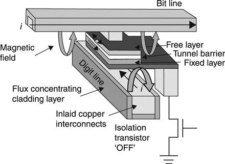
Up to the early 2000s, all the development efforts for MRAM technology with an architecture composed of one transistor and were MTJ cell based, 25 with an architecture composed of one resistor and one resistor (1 T/1 R). This technology relies on the adoption of a tunnel junction coupled to magnetoresistive materials that exhibit changes in the electric resistance when a magnetic field is applied. The MTJ is composed of a pinned magnetic layer, a tunnel barrier and a free magnetic layer (Fig. 1.8). Electrons spin, polarized by the magnetic layers, traverses the tunnel barrier. A parallel alignment of the free layer with respect to the pinned layer results in a low resistance state, while an anti- parallel alignment results in a high resistance state.25,26 Therefore, the storing mechanism consists of the permanent magnetization of the ferromagnetic material in the MTJ. The datum can be sensed as the resistance in the MTJ, which can be high (low current) or low (high current). The writing can be performed through the magnetic field produced by the current flowing in the bit- and digit-lines.
The non-destructive read with a very fast access cycle is the premise for high performance, equal-long read and write cycles, and for low power operation. Moreover, the structure is radiation hard with an unlimited read/write endurance, which makes MRAMs suitable for write intensive storage applications. The major MRAM disadvantage appears to be the high write current. While this technology has enough read current to guarantee a fast access time, it requires a very large write current (mA range), which increase power consumption. The current requirements become even more challenging when MRAM devices are scaled. In fact, since the data retention capabilities of MRAM memory cells is related to the total volume of magnetic material used in the free layer of the MTJ, it is expected that the capability to retain the stored information will be degraded in scaled devices, where the MTJ geometrical features are shrunk. It follows that suitable materials with higher magnetic coercitivity must be adopted to retain the data in scaled devices, thus demanding more current to be programmed and erased.
One of the key milestone for the development of MRAM technology was the introduction of the toggle-MRAM writing scheme, in order to obtain better program disturb immunity. With respect to the conventional MRAM, a toggle-MRAM employs a programming technique based on the current amplitude (as in conventional MRAM) and on the timing of the applied programming pulses. Only the correct sequence of pulses delivered to the selected cell is able to switch its magnetization, leaving all the other cells unchanged along the programmed bit line and word line. Starting from 2006, low-density (4–16 Mb) chips based on the toggle MRAM concept have been commercialized and are today available on the market for very specific applications. In order to mitigate the scaling issues of the MRAM concept, a novel programming technique has been investigated and is fuelling a renewed interest in MRAM technology. This new approach is based on the spin-polarizing effect originally predicted in 1996,27 in which magnetization orientations in magnetic multilayer nanostructures can be manipulated via a spin polarized current. The resulting technology, conventionally called Spin-Transfer Torque MRAM (STT-MRAM), is based on an MTJ structure where a current-induced switching caused by spin-transfer torque is exploited. This novel approach allows mitigation of some of the conventional MRAM issues; in particular for scaling, there are still several challenges that must be faced (e.g. self-read disturbance, writing times, cell integration). Today, the STT-MRAM developments are very active with prototypes of 64 Mb and 1 Gb at 90 nm28 and 54 nm,29 respectively. However, no volume production has been started.
1.4.3 Resistive memories
Resistive memories, usually called ReRAM, are a large class of memory concepts that store the information in the resistance value of the cell. All of them are electrically programmable, although they are based on different material classes and different proposed switching mechanisms:
• switching induced by material phase change in selected chalcogenide alloys (PCM);
• formation of metallic bridges by dielectric breakdown and bridge opening by thermal fusion;30
• ‘volume’ switching, e.g. by electronic charge transfer (redox) mechanisms;31
• switching of filament regions in the resistive material by electronic charge transfer (redox) mechanisms;32
• electrochemical growth and dissolution of metallic dendrites by solid electrolyte/electrode processes (programmable metallization cells, PMC).33
The resistive memory materials proposed in these concepts range from organic materials (rotaxanes and catananes, polyphenyleneethylenes, Cu- and Ag-TCNQ) to inorganic (chalcogenide alloys, perovskite-type oxides, manganites, binary transition metal oxides), while electrode materials comprise various metals as well as electronically conducting oxides and nitrides. Among the materials that exhibit a resistive switching phenomenon, oxide materials have been studied intensively.
On the basis of I–V characteristics, the switching behaviors can be classified into two types, unipolar (non-polar) and bipolar. In unipolar resistive switching, the switching direction depends on the amplitude of the applied voltage, not on the polarity. An as-prepared memory cell is in a highly resistive state and is put into a low-resistance state (LRS) by applying a high voltage stress, called the ‘forming process’. After the forming process, the cell in a LRS is switched to a high-resistance state (HRS) by applying a threshold voltage (‘Reset process’). Switching from a HRS to a LRS (‘Set process’) is achieved by applying a threshold voltage that is larger than the reset voltage. In the set process, the current is limited by the current compliance of the control system or, more practically, by adding a series resistor. This type of switching behavior has been observed in many highly insulating oxides, such as binary metal oxides. Bipolar resistive switching shows directional resistive switching, depending on the polarity of the applied voltage. This type of resistive switching behavior occurs in many semiconducting oxides, such as complex perovskite oxides.
It should be noted that there is a lot of speculation and controversy on the exact physical switching mechanisms for many of these concepts. Moreover, in many cases the role of the electrode materials is found to be important, although not entirely understood. However, independently of the mechanism, important basic characteristics for all concepts are represented by the required switching voltage and switching current. Indeed, low switching voltages are required to be compatible with the low supply voltages of scaled technologies, while low switching currents are required to be able to switch with minimal-size selector devices as well as to limit the switching power. For array fabrication, a transistor-type architecture is preferred, while the cross-point architecture and the diode architecture open the path toward stacking memory layers on top of each other and therefore are ideally suited for mass storage devices.
The largest advantage of ReRAM technology is its good compatibility with CMOS processes, in particular for binary-oxides based memories. The critical issues for the future development of ReRAM devices are reliability, such as data retention and memory endurance (the number of erase and program cycles), and the characteristic variation from cell to cell and from chip to chip. Despite the large potentialities showed by some of these concepts, the poor control of resistance distribution and the low maturity level reached by cell integration into sub-micrometric devices represent the main limitations for several of these concepts.
Some notable attempts to develop ReRAM should materialize in the few next years, as real commercial products. The availability of an evaluation kit, including a ReRAM memory fabricated in 180 nm technology, has recently been announced,34 while a 32 Gb ReRAM test chip, developed in the 24 nm process, with a diode as the selection device and a 2-layered architecture, has been presented.35 These interesting results make ReRAM one of the most promising alternative memory technologies for mainstream applications.
1.4.4 Phase-Change Memories
Among the different NVM, based on these mechanisms alternative to the floating-gate concept, Phase-Change Memories (PCM) are one of the most promising candidates to become mainstream NVM, having the potentiality to improve the performance compared to Flash (random access time, read throughput, direct write, bit granularity, endurance), as well as to be scalable beyond Flash technology.
PCM exploits thermally reversible phase transitions of chalcogenide alloys (e.g. Ge2Sb2Te5). Some alloys, based on the VI group elements (usually referred as chalcogenides), have the interesting characteristic to be stable at room temperature, both in the amorphous and in the crystalline phase. In particular, the most promising are the GeSbTe alloys, which follow a pseudo-binary composition (between GeTe and Sb2Te3), hereafter referred to as GST. The most interesting feature of these alloys is their capability to reversibly switch between a high resistance amorphous phase and a low resistance crystalline within a few hundreds of nanoseconds.
The basic cell structure is composed of one transistor and one resistor (1 T/1R) that can be programmed through current induced Joule heating, and can be read by sensing the resistance change between the amorphous and the poly crystalline phase. The PCM cell is essentially a resistor of a thin-film chalcogenide material with a low-field resistance that changes by orders of magnitudes, depending on the phase state of the GST in the active region. The switch between the two states occurs by means of a local temperature increase. Above the critical temperature, the crystal nucleation and growth occur and the material becomes crystalline (Set operation). To bring the chalcogenide alloy back to the amorphous state (Reset operation), the temperature must be increased above the melting point of hundreds of °C and then very quickly quenched down, in order to preserve the disorder and not let the material crystallize. From an electrical point of view, it is possible to use the Joule effect to reach locally both critical temperatures using the current flow through the material by setting proper voltage pulses. The cell read-out is performed at low bias. Programming thus requires a relatively large current, in order to heat up the GST and lead to a thermally induced local phase change. Phase transitions can be easily achieved by applying voltage pulses with different amplitudes and with durations in the range of tens of nanoseconds.
Although the phase change concept is well known and the first studies date back to the 1970s,36,37 its application for NVM was renewed in 1999, when the idea to have a semiconductor NVM cell based on the phase change of a chalcogenide material was presented again.38 Since then, efforts to bring the PCM basic concept to a mature technology level has constantly increased and many groups have started to study, develop and integrate the memory cell into MultiMegabit arrays.
The technology development roadmap of PCM is illustrated in Fig. 1.9. A 180 nm technology node has been used to develop the first demonstrator vehicles and to prove the technology viability.39 The BJT-selected cell has been chosen for the high performance and high density application, since the cell size can be around 5 F2 (where F is the minimum cell half-pitch). The MOS-selected cell is suitable for the system on a chip or embedded application,40 because in spite of the larger cell size (~ 20 F2) the memory integration adds only a few masks to the logic process with a clear cost advantage.

A 90 nm technology node has been developed and commercialized using a 128 Mb product.41 A 1 Gb PCM product fabricated at the 45 nm technology node with a cell size of 5.5 F2 has been developed and is in volume production for wireless application.6 This 45 nm PCM architecture42 demonstrates the maturity of the technology. The energy delivered to program a bit is in the order of 10 pJ, with a state-of-the-art access time of 85 ns, read throughput 266 MB/s and write throughput of 9 MB/s.43 These peculiar features combined with data retention, single bit alterability, execution in place and good cycling performance enables traditional NVM utilization but also novel application in the LPDDR field. Moreover, PCM is considered the essential ingredient to push to the market the so- called Storage-Class Memory (SCM),5 a non-volatile solid-state memory technology that is capable of filling the gap between CPU and disks (Fig. 1.1).
One of the key challenges of PCM cell scaling is the reduction of power, mainly due to the programming current. So far most of the development has focused on cell structure optimization, in order to increase the programming efficiency. More recently it has been shown that by proper engineering of the active material, it is possible to reduce the programming current of a standard PCM cell of 1/20,44 enabling even more low power innovative applications.
1.5 Beyond evolutionary architecture scaling
Planar NAND with MLC capability today represents the most cost-effective solution for an NVM concept. It can provide a minimum cell size of 4 F2 combined with MLC capabilities up to 3 bits-per-cell at the leading edge technology node of 20 nm, resulting in an effective cell size of 1.3 F2. It is clear that none of the alternative NVM so far discussed can be a serious contender as a NAND replacement in terms of cell costs. Although MLC has been proposed for some concepts (e.g. PCM41), its implementation and feasibility at the state-of-the-art lithography node is still to be demonstrated.
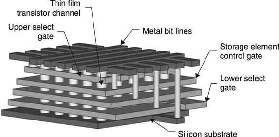
In this scenario and considering the growing difficulties that must be faced for planar NAND scaling, there is strong interest in the so-called 3D NVM technologies. There are currently two main trends to develop 3D structures that can provide a higher integration density: cross point memory array, where several memory layers can be stacked, and the so-called 3D NAND, where the standard NAND strings are integrated along the vertical dimension (Fig. 1.10).
While several ReRAM and PCM cell concepts are well suited for integration into a cross-bar memory array, the key challenge for researchers is the development of a suitable selecting device that can be integrated in close proximity to the cell. Such a selecting device is requested to provide a very low leakage when it is unselected, a high current in the on-state and a moderate voltage drop for turnin on. At the same time, there are several constraints for its fabrication; basically its suitability to be integrated into a CMOS back-end, low thermal budgets to allow stack-ability, and thin thickness to obtain a reasonable aspect ratio when combined with a 1Xnm pitch.
Three- dimensional NAND was originally proposed45 as a cost-effectivesolution for vertical NAND fabrication. The process is intended to use a minimum number of masks, thus reducing fabrication costs. However, a great deal of effort is required to develop the suitable integration modules in order to have at least 32 layers along the vertical dimension. Such a huge number of layers are needed to allow a 3D NAND with a relaxed pitch to be cost-effective with respect to the existing planar NAND. Recently it has been announced that 3D NAND technology will be commercialized starting from the SSD application, with 24 layers and MLC in a 128 Gb monolithic module.46
1.6 Future trends
The current NVM mainstream is based on Flash technology and it is expected that Flash will be in high volume NVM production within the next years. This technology is characterized by a compact structure in which the selecting element and the storage element are merged in a MOS-like architecture. The resulting full compatibility with the CMOS technology and the compact device size has made Flash technology the cheapest solution for stand-alone and embedded memory applications. However, discordant requirements to shrink the MOS structure preserving good selecting and storage capabilities are making Flash scaling increasingly difficult. Moreover, even if in the long term the cost advantage is important, better performance can speed up a novel technology introduction. In fact, a NVM with low power and low voltage capabilities, bit granularity, fast operations and higher endurance would be a potentially game changer for system designers.
To enlarge application segments, offering better performance and scalability, new materials and alternative memory concepts are mandatory to boost the NVM industry. In the last few decades, a total of more than 30 NVM technologies and technology variations compete for a piece of the fast growing NVM market, many of them aiming to replace DRAMs. Although planar NAND scaling is becoming harder and is obtained with several compromises in terms of reliability, state-of-the art NAND technology is 3 bits-per-cell 20 nm. Moreover, as already mentioned in the previous section, 3D NAND is becoming a mature technology. It follows that any NVM development must be able to provide the same capabilities at higher density. If this is not achieved in the next generation, technology scaling will not result in a cost reduction, thus stopping interest to continue in this direction. Cost structure is therefore a fundamental parameter for benchmarking novel NVM concepts, in particular for those that want to compete for data storage solutions, where MLC capabilities and/or 3D-stacking are mandatory.
On the other hand, the actual development efforts of alternative NVM concepts are demonstrating that disruptive innovation is time-consuming. Figure 1.9 reports the schematic development history of PCM technology, the only emerging memory concept that has reached the volume production maturity for a large density array. It is worth noting that the continuous need to stay close to state-of-the-art lithographic nodes combined with the necessary learning cycles require a decade of effort for moving from the concept to the mass production. Moreover, we also need to consider the time-to-market, i.e. the time needed to get a significant profit from a novel NVM technology. For the Flash NOR, about four years were required to reach the breakeven point with the EEPROM in terms of profit for the main semiconductor industries involved in this market. The scaling lesson was also clearly demonstrated by MRAM developments. MRAM products reached product maturity in correspondence with the last feasible technology node for the conventional toggle-MRAM, thus limiting the commercial success of MRAM technology and reducing it to a niche market. Only the discovery and exploitation of the STT-MRAM concept allows to forecast a better scalability below the 90 nm node, thus renewing interest in this technology. In this perspective, there are two major aspects that must be considered for evaluating the potentialities of any emerging memory concept:
If we combine the above two statements, it follows that any realistic proposal for a novel NVM technology must prove its feasibility for the sub-1Xnm technology node.