
Conductive bridge random access memory (CBRAM) technology
J.R. Jameson and M. Van Buskirk, Adesto Technologies Corporation, USA
Abstract:
How an emerging non-volatile memory fits into today’s landscape of existing memory technologies will depend on its performance, and this will partly depend on the physics governing the operation of an individual cell. We discuss the operating physics of the prototypical conductive-bridge random access memory (CBRAM) cell in analogy with the physical characteristics of atomic wires (i.e. quantum point contacts). The fundamental origin of key performance characteristics is highlighted and fit into the landscape of technological challenges and market opportunities laid out at the beginning of the chapter.
Key words
conductive-bridge memory; CBRAM; resistance-change memory; RRAM; quantum point contacts
10.1 Introduction
Memory is the engine for the digital world and semiconductor memory is preferred for its low power, ruggedness and reliability. Without these memories, handheld computing, cellular telephones and increasingly safer and lower emission automobttiles would not be practical.
Semiconductor prophets have long unsuccessfully forecast the demise of conventional semiconductor memory technologies such as Flash and DRAM. These predictions have been primarily based on the ability to physically scale the transistors associated with making the individual memory cells. Whether moving from planar structures to 3D (vertical or layered device), double (triple or quadruple) patterned lithography, or multiple bits per cell (MLC), incumbent memory technologies keep finding solutions. The ingenuity of engineers has kept these dire predictions at bay, finding methods to continue scaling, in keeping with Moore’s Law. However, the industry now faces a plethora of scaling limitations all converging toward the ‘brick wall’ long predicted by the prophets (Nishi 2011).
10.2 Scaling challenges in dynamic random access memory (DRAM)
The ITRS DRAM scaling rate no longer follows Moore’s Law (ITRS 2012). DRAM represents a digital bit by the charge stored on a capacitor. The dimensional or traditional Moore’s Law scaling challenges that face DRAM are how to retain this charge while reducing the storage node size and maintaining (or reducing) the loss of charge due to leakage through both the access device and the storage node itself (Kim 2009).
10.2.1 Storage capacitor scaling
Three cardinal parameters control DRAM storage capacitance scaling:
1. physical scaling: typically limited by lithography (Kim 2007), as discussed in Section 10.3.4;
2. capacitance per unit area of the storage capacitor: typically determined by the dielectric constant of the capacitor’s dielectric layer; and
3. bit-line capacitance: the ratio between bit-line capacitance and the storage capacitor capacitance determine the sensing signal strength.
These parameters lead to the buried word line (Schloesser et al. 2008) technology commonly practiced today in commercial DRAM. The challenges and requirements of physical scaling of the storage capacitor are well documented (Hong 2007), as are efforts to increase dielectric constant (ITRS 2012), and the authors would refer the interested reader to these publications.
10.2.2 Access device scaling
Efforts to control access device and storage node leakage, while further scaling the physical cell size, forced the introduction of the first commercial implementation of 3D transistors (Recessed Channel Access Transistor, RCAT) (Hong 2007; Kim 2007). This allowed scaling of the physical footprint without aggressively scaling the transistor effective channel length. Further improvements have included the introduction of Saddle FinFets and other innovations. However, the most intriguing innovation is the vertical access device (Goebel et al. 2002; ITRS 2012; Song et al. 2010; Yoon et al. 2006). With the advent of a vertical access device, the physical footprint reduces from 6F2 to 4F2 (Divakaruni 2011). The authors expect this innovation will have profound implications for emerging memory technologies.
10.3 Scaling challenges in Flash memory
Like DRAM, conventional Flash memory faces numerous challenges from dimensional or traditional Moore’s law scaling, including:
• how to maintain a reasonable minimum stored charge as the cell is scaled;
• electrostatic coupling to adjacent cells;
Other challenges also exist, such as random dopant fluctuation (which mostly affects the select devices), but a comprehensive summary is beyond the scope of this chapter. These four issues are summarized below. For more information, we refer the interested reader to several of the articles (Aritome 2011; Kim 2007; Nishi 2011; Prall 2007).
10.3.1 Minimum stored charge and MLC
Multi-Level Cell (MLC) approaches have greatly assisted both NAND and NOR Flash in maintaining density and cost scaling consistent with or exceeding Moore’s Law. At process nodes of less than 20 nm, the total stored charge is only approximately 20 electrons. This is just a few electrons more than the minimum of 16 electrons per bit required for MLC (Aritome 2011; Nishi 2011). Each electron represents approximately a 100 mV threshold voltage shift at the control gate. Much has been written regarding the limitation of MLC approaches as the process node falls below 20 nm (Prall 2007).
10.3.2 Electrostatic coupling
Similarly, much has been written regarding the challenges of floating gate to floating gate coupling between adjacent cells, requiring elaborate data programming schemes in an effort to mitigate them (Prall 2007). A key scaling constraint is the tunnel oxide, the thickness of which directly affects the retention of a Flash cell, and it has not scaled significantly since inception, staying near 10 nm (Kim 2007). Some have addressed this by using SONOS-like charge trapping technologies (Prall 2007). The smooth interface between the tunnel oxide and the silicon-nitride storage layer of a SONOS cell allows tunnel oxides as thin as 3.5 nm while preserving retention comparable to conventional floating gate devices. With the tunnel oxide thickness relatively fixed, to maintain proper floating gate to control gate coupling, the poly-poly blocking oxide thickness is also relatively fixed. These factors lead to cell-to-cell cross-talk (Prall 2007).
10.3.3 Voltage scaling
Since the tunnel oxide of a conventional Flash cell has not scaled significantly since inception, neither have the cell operating voltages. Both NAND and NOR Flash technologies require greater than 10 V to program and erase. The retention physics of the technology thus prohibits significant voltage scaling. As NAND technology enters the sub-20 nm regime, the WL-WL dielectric thickness is of the same order as the floating gate to control gate dielectric thickness, resulting in WL-WL leakage, enhanced by the line edge roughness of the WL (Aritome 2011). The inability of NAND and NOR Flash memory to scale operating voltages is a key weakness that an emerging memory could exploit to gain a foothold in the market.
10.3.4 3D Flash and the limitations of conventional lithography
The limitations of conventional lithography to print minimum feature sizes apply to conventional and emerging memories alike. These have been detailed in numerous articles (Kim 2007) so will not be repeated here, except to provide the following brief outline of which lithography tool provides features of a given size:
• 193 nm immersion tool limitations (Kim 2007):
– Conventional = ~38 nm in theory, 43 nm in practice;
– Double attern/double printing = ~19 nm in theory, ~22 nm in practice;
– Quad patterning/printing = ~10 nm in theory, ~15 nm in practice,
– EUV will use a 13.5 nm light source;
– In theory, will be able to directly print features at ~14 nm.
While EUV tools are in principle capable of directly printing features for sub-20 nm nodes, their cost, complexity and limited throughput thus far prevent such usage for manufacturing. The lack of a lithographic solution for the advanced nodes has been a driving force for 3D Flash development (Aritome 2011), in which N layers of cells are patterned all at once. In this way, bit densities can be achieved that are higher than achievable with the cells in a single layer. Though 3D stacking is still limited by lithography and a practical number of charge trapping layers (with somewhat degraded, but manageable, array efficiency), it is an operational means to extend the effective density of Flash memory beyond 16 nm, while at the same time lowering cost. While conventional Flash plans to first commercialize 3D integration, the authors expect 3D integration utilization in future for emerging memories as well.
10.4 Marketplace challenges for emerging memory technologies
Given the scaling challenges of these incumbent memory technologies, the industry is feverishly pursuing alternate memory technologies, setting the stage for the market entry of emerging memory technologies (Kim 2007). Many speak of a ‘universal memory’ with the write speed of an SRAM and the retention and cost structure of Flash – a memory to replace all conventional memory. This ‘Holy Grail’ of memory may not be achievable in practice and should not be considered a requirement for an emerging memory technology. As with conventional memory technologies, the market accepts limitations and shortcomings for cost, performance and non-volatility.
Market acceptance is the largest challenge for anything new. Users are afraid or unwilling to accept the risk of untried, untested technology on their already complex products. The best-modeled reliability, with reams of supporting data, may not be sufficient – the technology is new. To bridge this divide, there must be a compelling reason (or application) to risk using unproven technology over incumbent technologies. There needs to be a special attribute. The cost-effective ‘in-system re-programmable’ attribute of NOR Flash, for example, made rapid software upgrades possible during the early evolution of Europe’s GSM cellular network. Such attributes as low power, lightweight and rugged non-volatile storage of NAND Flash, as another example, enabled the handheld computing revolution we are now experiencing.
10.4.1 Scalability
Besides offering a special attribute, scalability is clearly a desirable attribute for an emerging memory to have, given the reported shortcomings of incumbent technologies. However, achieving a cell size cost equivalent to incumbent technologies may not be initially practical. First, this is a moving target. Second, this requires use of leading edge technologies and factories, often dedicated to existing revenue-bearing products. Instead, it is often sufficient to merely theoretically demonstrate cost competitive future scaling. However, even a theoretical demonstration may be challenging.
10.4.2 Blocking device challenges
While the industry and scientific communities have focused extensively on the switching characteristics of emerging memory, until recently little attention has been afforded to placing the switching element in a matrix. All emerging memory devices require either an access or blocking device. If this device is a conventional MOS, BJT (Wang 2011) or single crystal structure, technology scaling suffers the same limitations of incumbents. Similarly, current requirements for many emerging technologies may exceed both scaled access device and scaled interconnect current density capabilities. However, these conventional devices are well understood and offer respectably abrupt on/off characteristics.
In contrast, a minimum stackable true cross-point array memory cell requires either a thin film or built-in access device. While this, in theory, achieves the requisite cell size, it also places tremendous pressure on device, interconnect and array architecture to achieve scalable functionality (Yoon et al. 2009). The simplest thin film device is a diode (Wong 2008; Lee et al. 2007a,b). Diodes, in general, do not afford sufficiently abrupt on/off characteristics to adequately inhibit read or write disturbs to unselected switching elements within a large matrix (Toda 2009). Many emerging technologies require reversing the electric field and/or current flow in order to reverse state (HRS vs LRS) (Kozicki 2011). This requirement places a further constraint on an already challenging thin-film access device requirement.
Recent work (Chevallier et al. 2010; Kim et al. 2012; Lee et al. 2010) has focused on using the abrupt switching behavior of many emerging memory devices as the access device. This, in principle, provides the requisite selection properties. However, these technologies can also have memory effects? the access device will not deselect immediately, determined by the retention time constant of the device. As with all retentive devices, there is a large distribution in this retention time constant. For the switching element, we are constrained from only one side, namely the short time constant. For an access device, the retention time constant must be greater than the read or write access time and short enough for practical read and write cycle times.
Similarly, achieving cell size without the capability to pattern all films (access device and memory device) within the stackable array in a single pass (i.e. those proposed by 3D vertical NAND) will, in all likelihood not be cost-effective. This is due to the high cost and limitations of 193 nm (wet) lithography forcing more complex (and expensive) multiple pass patterning techniques. Memory process nodes of less than 40 nm currently must make use of these techniques. In all likelihood, this will continue indefinitely given the slow progress bringing cost-effective EUV lithography into production. Inevitably, the problems of the switching element and the access device will be separated, with initial emerging memory products using conventional MOS, BJT or single crystal access devices (Zhang et al. 2009). These initial products must then achieve market acceptance with attributes other than cost.
10.4.3 Performance
Most emerging memory technologies afford significant performance advances over incumbent technologies. Notably, nearly all technologies offer retention time constraints of hours, if not years – far exceeding DRAM. Similarly, the write times of many of these technologies are 10 to 100 ns – far exceeding Flash.
10.4.4 A new class of memory products
There is a huge product space between tens of nanoseconds read/write times and hundreds of milliseconds retention times of DRAM and the microsecond to millisecond write times and multiple year retention times of Flash. Few NVM applications truly require multiple year retention times, given periodic access to power. Similarly, compromising DRAM read/write times for much longer refresh times could be an option. Combining these properties, we have a device with characteristics between DRAM and Flash. This is not the ‘universal memory’, but it is useful. This product space is often referred to as ‘Storage Class Memory’ (Burr et al. 2008; Freitas and Wilcke 2008). While largely undefined to date, the properties of many emerging technologies make such memory products practical.
10.4.5 Leveraging incumbent technologies
As with any new endeavor, introducing a new technology is wrought with challenges, hurdles and unknowns. There is often the temptation to reach immediately for the highest possible goal. While this may be admirable, without first establishing a strong technology basis, this approach is likely to fail. Instead, leveraging incumbent technologies for access devices substantially reduces the number of challenges (Zhang et al. 2009).
10.4.6 Fab friendly
The use of fab-friendly materials is highly desirable, but not an absolute requirement. This allows the leveraging of existing materials understanding, deposition and etching techniques. If new materials are used, a manufacturing infrastructure must be established. Similarly, CMOS contamination, thermal and stress compatibility must all be demonstrated. Again, in order to maintain compatibility with standard CMOS BEOL process flows, the entire emerging memory system should be stable through these temperatures.
10.4.7 Packaging and board assembly
Product packaging and subsequent printed circuit board (PCB) mounting are essential, but often overlooked, issues for emerging memory. Unlike the BEOL thermal stability requirement, typical applications encapsulate the memory in a plastic package and users of non-volatile memory often write data into the device prior to mounting on a PCB. Of course, the memory cell functionality and any data written prior to PCB mount must remain post packaging and PCB mounting. Packaging mold temperatures are approximately 180 °C for about 6 hours. Similarly, the IR solder reflow process commonly used throughout the industry for PCB mounting ramps to approximately 260 °C for about 3 min. Many emerging technologies, such as PCRAM, struggle with this issue (Choi et al. 2012; Kim et al. 2010; Neale 2012).
10.4.8 Embedded vs. stand-alone
A major advantage of emerging memory is the ability to relatively easily integrate the memory with existing logic technologies. Of the incumbent technologies, only SRAM (and to some degree OTP/MTP oxide breakdown technologies such as Kilopass and Sidense) offers this capability (Kilopass; Sidense). While interest in embedded memory is strong, without the commercialization of stand-alone products, few, if any, System-on-Chip (SOC) companies would risk critical products to an unproven technology. Thus, stand-alone products prove technology viability. Both stand-alone DRAM and Flash preceded embedded applications.
10.4.9 Application requirements
Handheld computing, whether smart phones or tablets, strongly prefers solid-state storage. The ruggedness, weight, size and power requirements rule out mechanical alternatives such as HDD. Industrial applications (i.e. machinery, computer servers and communications equipment) require reliability and ruggedness, while automotive under-hood applications, in addition to reliability and ruggedness, also require operating temperatures exceeding 175 °C.
10.5 Operation of a CBRAM cell from an atomic wire point of view
How an emerging non-volatile memory fits into this technological landscape will depend on its performance, and this will depend, at least in part, on the physics governing the operation of an individual cell. In this section we discuss the operating physics for what might be considered the prototypical CBRAM cell, which is a cell having a parallel-plate structure with an elemental Ag or Cu anode, an insulating layer made of a Ag- or Cu-conducting solid electrolyte, and a cathode made of a metal that does not dissolve into the electrolyte under normal operation conditions (Kozicki et al. 2004). A patent relating to such a cell, originally referred to as a ‘programmable metallization cell,’ was first issued in 1998 to Michael Kozicki and William West of Arizona State University (Kozicki and West 1998). Later, Ag- and GeS2-based cells were developed by Adesto Technologies Corporation of Sunnyvale, CA under the trademark CBRAM (Adesto and CBRAM are Trademarks of Adesto Technologies Corporation). In 2012, Adesto Technologies offered a CBRAM chip for sale as a low-density EEPROM replacement, making it the first time any such resistive memory (RRAM) had been brought to market.
It is well established that the basic mechanism of switching in a CBRAM cell is the making and breaking of a small metallic filament of Cu or Ag. Early experiments carried out by Michael Kozicki, his students and post-docs at Arizona State University clearly demonstrated these phenomena. They constructed a cell in which the anode and cathode were both deposited on the surface of the electrolyte, forming a lateral device that allowed the ‘active’ region between the electrodes to be imaged by an optical microscope during electrical operation (West et al. 1998). Kozicki and his students observed that applying a positive voltage to the anode caused a dendritic ‘filament’ to grow from the cathode to the anode, whereas a voltage of the opposite polarity caused it to dissolve away, beginning from the anode. Because the experiment used an optical microscope it was not possible to investigate the shape of a filament at length scales below about 1 μm, or to investigate sub-micron cells. Attempts were made in subsequent experiments to use a scanning-electron microscope (SEM), but it was found that the electron beam of the SEM caused the metal atoms inside the solid electrolyte to move, making metallic ‘mushrooms’ grow from the surface (M.N. Kozicki, private communication).
Recently, electrical measurements (Section 10.6.1) have shown that the filament in a prototypical cell can be extraordinarily small, even as narrow as a single atom at its thinnest point. A CBRAM cell in the ON state may thus be envisioned as two macroscopically large pieces of metal (the anode and cathode) connected by a short (the thickness of the insulator) metal wire that is atomically thin (at least at one point). This bears an undeniable resemblance to the quantum point contacts that have for more than 20 years been studied in the physics community, and which have traditionally been fabricated by mechanical methods such as mechanically controlled break junctions (MCBJs) (Agraït et al. 2003). We may expect that the electrical characteristics of quantum point contacts would be reflected in the electrical characteristics of a CBRAM cell, and the present section is aimed at drawing this analogy. A single chapter is not sufficient to describe all such characteristics, however, and we focus here on just a few that are particularly interesting or important.
The authors believe the physics of quantum point contacts to be as central to the understanding of CBRAM cells as the physics of the field effect is to the understanding of MOSFETs. Yet, an ‘atomic wire’ point of view cannot address every important characteristic of a cell. Issues not addressed include such things as the physical processes and kinetics governing filament growth, the impact that the choice of electrolyte has on the performance of a cell, or the causes of errors. The authors would refer the reader to the literature on CBRAM for a discussion of these and other issues, such as the review articles which now exist (Valov et al. 2011; Waser 2009). Likewise, the authors do not intend this section to be a tutorial on the physics of quantum point contacts. For that, they would direct the reader to the excellent review by Agraït et al. (2003), which is cited heavily here.
10.6 The ON state of a CBRAM cell and the programming operation
10.6.1 Quantized conductance and the size of the filament
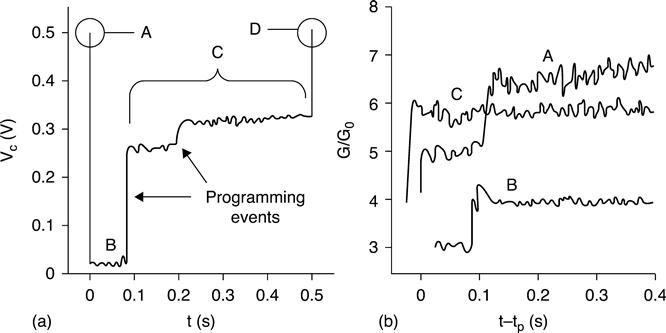
The key observations which established (Jameson et al. 2011, 2012a) that the filament in a prototypical CBRAM cell must be of atomic dimensions, at least at its narrowest point, were that abrupt changes in conductance occur during a programming operation, and that the value of the conductance in between abrupt changes tends to be an integer multiple of the fundamental conductance G0 = 2e2/h. An example of this is shown in Fig. 10.1 for the W/GeS2/Ag CBRAM cells described by Gopalan et al. (2011). The extremely fast programming speed of CBRAM cells can make these abrupt changes difficult to observe, especially at high programming voltages, and it was the use of a custom circuit integrated on-chip with the CBRAM cells that enabled these measurements to be made readily. Especially important was that the settling time of the output circuitry was short enough (~40 ns) to allow the periods of time between jumps to be resolved with confidence. These regions were often found to be flat, or nearly flat (Fig. 10.1), which suggests that the filament, or at least the portion of the filament that sets its conductance, is developing in a sequence of discrete events, not in a continuous manner. The fact that the plateaus tend to be at integer multiples of G0 indicates that the conductance of the cell must be set primarily by a very narrow constriction, as in a quantum point contact. Moreover, it is known that point contacts of Ag or Cu yield conductance very near the integer values of G0 (Agraït et al. 2003). That the Ag/GeS2/W cells yielded integer values of conductance, as opposed to half-integer or fractional values, is thus fully consistent with the metallic path being made of Ag, as Kozicki concluded in his experiments.
10.6.2 Ultimate scalability of CBRAM
An obvious consequence of the small size of the filament is that we should not expect the ON-state resistance to depend on the area of a cell, as this is always large compared to the ‘size’ of an atom. A lack of area dependence has of course been observed for many years in a variety of different CBRAM cells (e.g. Ag/GeSx/W cells (Symanczyk et al. 2003) and Ag/GeSex/W cells (Kund et al. 2005)), and it has often been said that this characteristic alone is sufficient to prove that the switching is filamentary. The counter-argument (Valov et al. 2011) is of course that the ON-state resistance is normally found to depend on the maximum current allowed to flow through the cell during programming, so a lack of area dependence is a self-fulfilling prophecy when cells of different sizes are all programmed at the same current level. Put differently, if we were to assume a priori that the conduction through a cell is describable by RON = ρL/A, we could not tell if it is the resistivity ρ or the area A of the conductive path that is altered by the programming operation. However, this counter-argument is made moot by the knowledge that the filament is atomically small. The presence of a filament is indeed the correct interpretation of the lack of area dependence in RON.
10.6.3 Temperature dependence of RON
Quantization of the conductance implies ballistic transport, and we should therefore expect the ON-state resistance of the cell to be independent of temperature, as in a quantum point contact (Sirvent et al. 1996 and Costa-Krämer et al. 1997 for Au point contacts). This was investigated by Betty Young (Young et al. unpublished) and her students at Santa Clara University using the same Ag/GeS2/W CBRAM cells (Gopalan et al. 2011), in which the quantized conductance was first observed (Jameson et al. 2011, 2012a). CBRAM cells lacking any access circuitry (e.g. a transistor) were used so as to avoid spurious sources of temperature dependence. The CBRAM cells were programmed at room temperature to resistance levels on the order of kΩ, then cooled to 77 K in a cryogenic refrigerator under a constant bias of 50 mV. The temperature of the sample stage and the current through the cells were both recorded as a function of time during cooling. The resulting plot of resistance vs temperature is shown in Fig. 10.2(a), where the resistance has been normalized to its value at room temperature. The resistance of the cells is seen to change by no more than about 7% between room temperature and 77 K, as compared to the 4× change that would have resulted had the filaments in the cells exhibited the 1/T dependence of bulk Ag. This result actually preceded the observations of quantized conductance in such cells, and it provided confirmation of the picture of the filament as a quantum point contact.

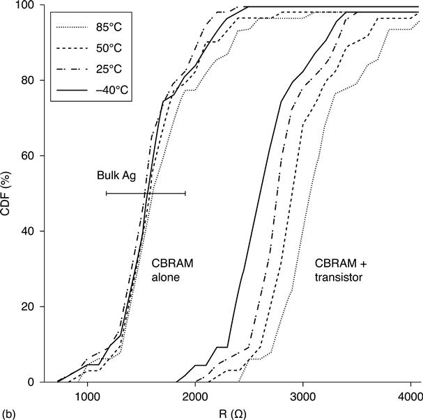
Cryogenic measurements have the advantage of providing a large change in kT, but they have the disadvantage of being time-consuming and therefore difficult to perform on large numbers of devices. This may make the conclusion that the ON-state resistance of a cell is independent of temperature seem unconvincing, especially if we are expecting to observe the 1/T dependence of bulk Ag. In a subsequent measurement, the lack of temperature dependence was verified using hundreds of integrated ‘1T1R’ devices (i.e. a CBRAM cell in series with a transistor) and a standard probe station whose chuck temperature was varied between −40 °C and 110 °C. The resistance of a representative sample of bare transistors was measured independently over the same range of temperature, and the median resistance of the transistors at a given temperature was subtracted from the total resistance of each of the 1T1R devices. The resulting resistance, which represents that of the CBRAM cells themselves, is plotted in Fig. 10.2. The change in resistance is again found to be small, confirming the conclusion from the cryogenic measurements, except for about 1% of the cells, which suffered permanent changes after multiple thermal cycles.
10.6.4 Current-voltage characteristic
The current-voltage characteristics of quantum point contacts are typically found (Agraït et al. 2003) to contain power-law nonlinearities (e.g. I = c1V + c3V3, with c1 and c3 constant), and this represents a third characteristic we may expect to observe if the ON state of a CBRAM cell does indeed behave as a quantum point contact. To the authors’ knowledge, however, no detailed reports exist on the IV curves of prototypical CBRAM cells. This is perhaps surprising, given that an IV curve is the defining characteristic of a two-terminal device. The complicating factor is, of course, that a CBRAM cell is designed to change under bias, so that an IV curve can be altered by the act of measuring it. However, by using short voltage pulses and/or working at low temperature, the authors expect that reliable measurements should be possible, and if a careful study is carried out, they expect power-law nonlinearities to be observed.
10.6.5 ON-state series resistance
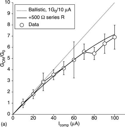
A fourth characteristic of the ON state, which appears consistent with the view of the filament as being a point contact, is the existence of an apparent series resistance associated innately with the filament itself. This series resistance, which has not been reported previously, is demonstrated in Fig. 10.3(a). CBRAM cells controlled by the same integrated circuit mentioned in Section 10.6.1 were programmed to different conductance levels by varying the maximum current Icomp allowed to flow through the cells immediately following a constant-voltage programming step. The resulting ON-state conductance GON is shown as a function of Icomp in Fig. 10.3(a) for a programming voltage of 0.50 V. At low compliance, GON increases linearly by 1 G0 for each increase of 10 μA in Icomp, but at high compliance a sub-linear dependence on Icomp is observed. The dashed line in the figure shows that this sub-linearity is close to that which would have obtained if a resistance of 500 Ω were placed in series with a filament whose conductance continued to increase by 1 G0 per 10 μA across the whole range of Icomp. However, the test circuit did not contain such a series resistance, meaning this apparent series resistance must be associated with the cell itself. The value of the series resistance that best matches the data is 500 Ω, though 900 Ω was found to be the optimal value after the same group of cells was cycled on and off several more times. This change again indicates that the resistance is not associated with the circuit, as the circuit does not change as the cell is cycled.
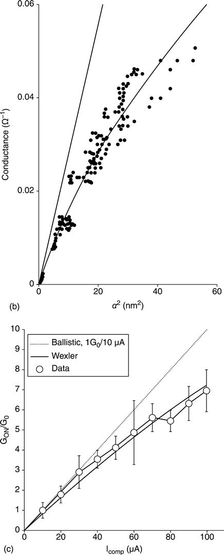
This phenomenon is reminiscent of the sub-linear dependence of conductance on the cross-sectional area that arises in point contacts due to elastic scattering near the constriction (Agraït et al. 2003). This was measured in Au point contacts by Erts et al. (2000), whose data is reproduced in Fig. 10.3(b). Erts et al. (2000) fit this data to the semi-classical Wexler formula GW = GS[1 + 3π/8Γ(Le/α)(α/Le)]−1, where Le is the elastic mean free path, α is the radius of the constriction, Γ is a function that varies from Γ (0) = 1 to Γ(∞) = 0.7, and GS is the semi-classical Sharvin conductance, which describes ballistic transport but not its associated quantized conductance. Knowing the radii α of the point contacts, Erts et al. (2000) obtained an elastic mean free path of Le = 4 nm for Au points contacts, which is similar to the value inferred from measurements of conductance fluctuations (see discussion by Agraït et al. 2003). Comparably small values (Le = 4 – 7 nm) were obtained by Ludolph and van Ruitenbeek (2000) for Ag point contacts, which are the direct analogue to the Ag filaments of the CBRAM cells used to produce the data in Fig. 10.3(b).
We may ask if the Wexler picture of elastic scattering in point contacts provides a reasonable interpretation of the sub-linearity observed in Fig. 10.3(a). Figure 10.3(a) plots the conductance of the cells vs current compliance, whereas the Wexler formula provides conductance as a function of radius. The Wexler formula cannot therefore be fit in to Fig. 10.3(a) directly. However, the axis of Fig. 10.3(a) can be transformed, at least approximately, from current compliance to cross-sectional area if we assume that the number of atoms per unit area across the constriction of the filament is of the same order of magnitude as the number of atoms per unit area on a surface of bulk Ag. It is known (Agraït et al. 2003) that a 1-atom constriction of Ag yields a conductance of nearly G0, so the slope of 1 G0 per 10 μA in Fig. 10.1 may be restated as 1 atom per 10 μA. A surface of bulk Ag contains on the order of 1 atom per 10 Å2, giving a scale factor for Fig. 10.3(a) of about 1 Å2/μA. With this value, and taking the straight line in Fig. 10.3(a) to be the Sharvin conductance, fitting the Wexler formula to the data in Fig. 10.3(a) yields a mean free path of 2 nm, which is close to values reported by Ludolph and van Ruitenbeek (2000). This value of Le = 2 nm should be viewed as only an order-of-magnitude estimate, but we would note that obtaining a value larger or smaller by an order of magnitude would require us to choose unrealistic values when converting the horizontal axis from current to area. For example, fitting the data with a mean free path of 0.2 or 20 nm would require a surface density of 10 or 0.001 atoms/Å2, respectively, which are non-physical. An interpretation of the apparent series resistance in Fig. 10.3(a), as arising from elastic scattering near the constriction in the filament, thus appears to be reasonable.
10.7 The OFF state of a CBRAM cell and the erase operation
Because it corresponds to the lack of a continuous metal filament, we might not expect the physics of quantum point contacts to be useful in understanding the OFF state of a CBRAM cell, or the erase operation. However, a variety of characteristics of CBRAM cells do appear to be readily understood from this perspective.
10.7.1 Polarity of the erase operation
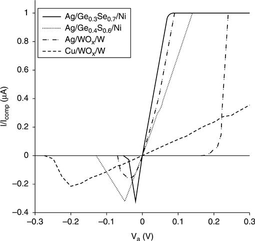
In the ON state, it is well known that the current-carrying capacity of a prototypical CBRAM cell is greater in the forward direction (i.e. anode positive) than in the reverse direction. A ‘butterfly curve’ obtained by measuring the current as the voltage is swept positive and negative thus appears asymmetrical for several types of prototypical CBRAM cells (Fig. 10.4). For negative voltages, the abrupt drop in current indicates that the cell has erased, and the key question is why this does not occur at a positive bias of equally small magnitude.
For a ballistic point contact, it is understood that the electrical resistance arises from scattering within the diffusive leads contacting the constriction, not within the constriction itself. An electron conducted ballistically across a point contact biased at voltage V will acquire a kinetic energy eV. The electron will carry this energy from one lead to the other, and will lose it to the lattice by inelastic scattering at a distance from the constriction on the order of the inelastic mean free path. In a CBRAM cell, the physical center of the heating associated with this inelastic scattering will therefore depend on both the location of the constriction along the length of the filament, and on the polarity of the applied bias.
It is understood that the filament in a CBRAM cell grows from the cathode to the anode. This was proven in Kozicki’s original experiments on lateral cells (Section 10.4.9), and has been shown theoretically to agree with a considerable amount of data on the kinetics of the programming operation (Jameson et al. 2011, 2012b). Near the surface of the anode is where it is natural to expect the constriction of the filament. Under forward bias (i.e. node positive), the kinetic energy of the electrons will therefore be deposited into the anode, whereas under reverse bias it will be deposited into the filament. Since the filament is surrounded by an insulator and since its mass is very small compared to that of the anode (which is a bulk-like continuous Ag film), a negative bias should therefore produce a larger increase in temperature in the filament than a positive bias. The atomic rearrangements associated with the rupture of the filament, which must be thermally activated, should therefore occur faster under a negative bias than under a positive bias.
It is interesting to contrast this picture with one in which the filament is viewed as a classical, diffusive conductor obeying the equation R = ρL/A. In this case, the same increase in temperature would occur for both polarities of bias, inducing no asymmetry (though the same cannot be said for electro-migration). Discussions of the role that Joule heating plays in the erase operation of CBRAM cells are widespread in the literature. However, a mathematical treatment of the erase operation from the present point of view has not yet been attempted, and represents an important avenue for further work.
10.7.2 Jump to contact and the forbidden zone
From our discussion of the ON state, it may be clear that the ‘natural’ operating window of the prototypical CRAM cell is bounded on the low end (i.e. the maximum ON-state resistance) by the fundamental conductance G0, which corresponds to a resistance of 1/G0 = 12.9 kΩ. However, it is not so clear as to what sets the high side of the window (i.e. the minimum OFF-state resistance), or even if a ‘natural’ upper bound exists at all. The physics of quantum point contacts offers insight into this question.
The key concept is that of ‘jump to contact,’ which has been studied using mechanically controlled break junctions (MCBJs) and other mechanical means of forming metallic point contacts (Agraït et al. 2003). As the piezoelectric voltage of an MCBJ is adjusted so as to bring the two tips of metal increasingly closer to one another, there comes a moment when the forces between the atoms on the surfaces of the tips become strong enough that an abrupt atomic rearrangement occurs, suddenly bringing the tips into contact. This jump to contact completes the metallic path, and the conductance immediately takes on one of the quantized values characteristic of a point contact of that metal. For many metals, the jump occurs from a resistance on the order of 100 kΩ. This resistance is due to tunneling across the gap between the tips, with the gap at the moment of the jump often being on the order of an Angstrom.
To relate this picture to the erase operation of a CBRAM cell, let us imagine that the heating produced by an erase operation, as described above, has caused a sudden atomic rearrangement that has created a gap in the filament. If the size of the gap is less than the distance from which the jump to contact typically occurs, then the two tips of the filament will be spontaneously pulled back into contact, reconnecting the filament and returning the cell to the ON state. To obtain a stable OFF state, the erase operation must therefore open a gap that is larger than the distance from which the jump to contact typically occurs, and the minimum stable OFF-state resistance of the cell will, on average, be the resistance associated with this minimum gap. That is, we may expect there to be a ‘forbidden zone’ of resistance which a prototypical CBRAM cell will tend to ‘avoid.’ To the extent that experiments on bare metallic point contacts (which are suspended in vacuum or in air) are representative of the filament of a CBRAM cell (which is surrounded by a medium, such as GeS2), we should expect this forbidden zone to start at a resistance of about 12.9 kΩ (or perhaps 12.9/n kΩ) and extend to a resistance on the order of 100 kΩ.
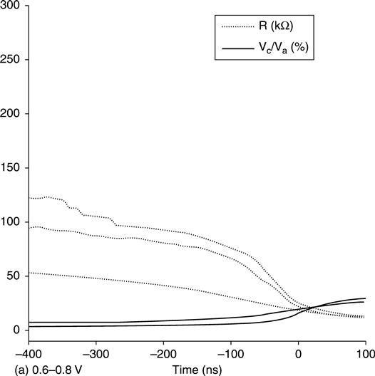
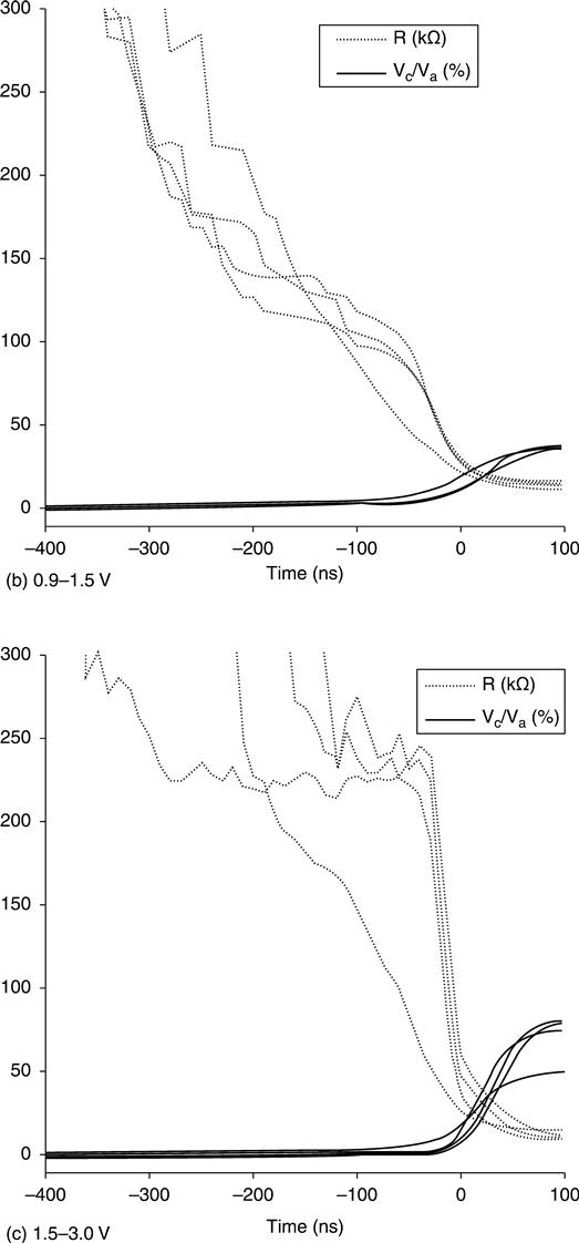
For Ag/GeS2/W cells, electrical data is available that indicates that a forbidden zone does indeed exist. It is observable, for example, when the resistance of a cell is plotted as a function of time during a programming operation, which can be accomplished using the same specialized circuit mentioned in Section 10.6.1. Figure 10.5 shows examples of this measurement. The key observation is that after dropping to a level on the order of 100 kΩ, the cells move to a resistance below 12.9 kΩ by means of a single abrupt jump. The resistance from which the final drops occurs seems to depend slightly on the programming voltage, but the dependence is weak, and the cells appear to be ‘avoiding’ resistances between about 10 kΩ and 100 kΩ. We note that although Fig. 10.5 makes it appear as though the resistance of a cell passes smoothly through the forbidden zone, it must be understood that even a truly instantaneous change in resistance would produce an output that varies smoothly over this timescale, as the slew rate of the output op-amp used in the circuit was a few tens of ns.
The practical importance of the forbidden zone is that it puts bounds on the verify levels that should be used for program and erase operations. That is, to ensure that a cell does not suffer a spontaneous OFF-state retention loss, the verify level for the erase operation should be set to a value no lower than the top of the forbidden zone. Likewise, to ensure that a program operation has formed a complete filament, a verify level of no less than bottom of the forbidden zone should be used. This provides a rule of thumb regarding the verify levels, though other considerations (e.g. endurance) inevitably come into play when determining the optimal values.
10.7.3 A minimum programming time
To bring us full circle, we consider the amount of time required to return the OFF state to the ON state via a programming operation. We highlight two aspects of this problem, both of which appear to be consistent with the existence of the jump to contact phenomenon and its associated forbidden zone. First, there appears to be a minimum time required to program a cell. The reason, we argue, is that programming a cell requires the gap in the filament to be closed, so the larger the gap, the more atoms and the more time will be required to do so. That a minimum gap is needed to have a stable OFF state (due to the jump to contact phenomenon) implies that a minimum programming time must exist. Second, a large collection of cells exhibits a distribution of programming times, which extends from this minimum programming time upwards to some maximum time, which is a function of the manner in which the cells were put into the OFF state. We argue that when a gap is first opened in the filament, a ‘recoil’ effect happens whereby the two ends of the filament collapse upon themselves, creating a gap larger than that which was initially opened. Such an effect is observed in MCBJs, as indicated by the fact that the metallic connection of an MCBJ cannot typically be reformed until the piezoelectric element is returned past the point at which the break occurred. That is, a hysteresis exists in the piezoelectric voltage required to make and break the point contact.
These two effects are illustrated in Fig. 10.6, which shows the time required to program two populations of Ag/GeS2/W cells that have been erased by two different methods. The programming time is seen to decrease with programming voltage, but a distribution is seen at every voltage. The cells in Fig. 10.6(b) have been erased ‘deeper’ than those in Fig. 10.6(a), resulting in their distribution extending upwards to programming times almost as long as those of virgin cells. However, the bottom of the distribution is essentially the same as that of Fig. 10.6(a), indicating that the minimum programming time represents an innate characteristic, as we would expect the minimum stable gap should be.
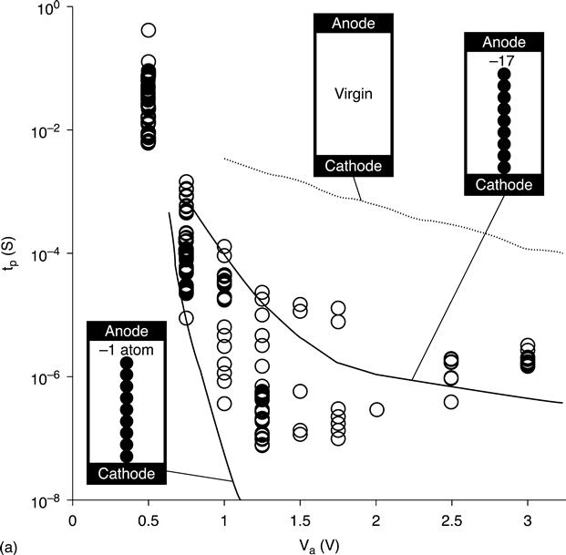
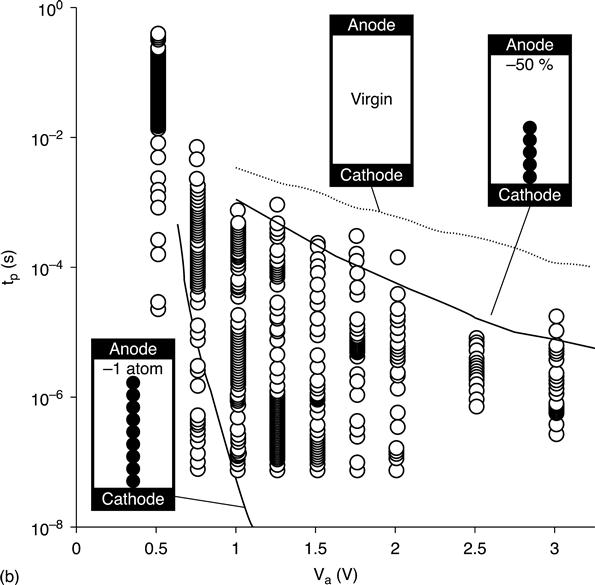
A recent model describing programming treats the filament as a monatomic chain that grows by injected ions one-by-one from the anode into a 1D potential that represents the solid electrolyte. This model allows us to quantify the gap sizes corresponding to the tops and bottoms of the distributions in Fig. 10.6. In the case of a virgin cell, the 1D potential is completely empty at the beginning of the programming operation. For a previously cycled cell in the OFF state, we propose here to model the broken filament by removing N atoms from its anode end (Fig. 10.6). The calculation then proceeds as for a virgin cell, using exactly the same parameters as for virgin cells (Jameson et al. 2011, 2012b), only now the programming time will depend on the number N of atoms that have been removed. The minimum possible programming time is obtained by removing just a single atom (N = 1), and it is seen that the programming time calculated for this case agrees well with the bottom of both distributions in Fig. 10.6. For the tops of the distributions, 17% of the atoms must be removed to match the data in Fig. 10.6(a), whereas 50% of the atoms must be removed to match the data in Fig. 10.6(b). This provides upper bounds on the sizes of the gaps. We note that the shapes of the tops of the two distributions are qualitatively different. Yet, the calculations agree well with the experimental data, indicating both that the model is correct, and that the anode-end of the filament is the proper place to locate the gap.
10.8 Conclusion and future trends
Market acceptance is the largest challenge for any new technology. To overcome the risk (real or perceived) associated with an unproven technology, the new technology must offer a compelling attribute (or application) that the incumbent technologies do not. This need is balanced by the recognition that the market will accept practical limitations for a new technology, just as it did when the incumbent technology was new. We have shown that the analogy with quantum point contacts provides a coherent viewpoint from which a wide variety of physical properties of the prototypical CBRAM cell can be understood. What then are the compelling attributes and practical limitations that these ‘atomic-wire properties’ give to CBRAM?
The most basic (and obvious) ‘atomic-wire’ attribute of CBRAM is its scalability. We have seen (Section 10.6.1) that even in ‘large’ CBRAM cells (i.e. ~100 nm diameter), the current in the ON state is carried by a filament that is only a few (or even just one) atoms wide at its thinnest point. The basic operational requirement of maintaining a low ON-state resistance can thus be satisfied down to cell sizes at the atomic scale. Practical limitations, particularly lithography (Section 10.3.4), become severe long before then, and in this sense the basic switching mechanism of a CBRAM cell is expected to present no significant roadblock to scalability. An atomic-wire filament can support a single conductance channel (yielding an ON-state resistance of 1/G0 = 12.9 kΩ) when its diameter becomes comparable to the Fermi wavelength in that metal. For Ag or Cu, this is on the order of the size of a single atom (Agraït et al. 2003). We may thus trace this attribute of CBRAMbn – extreme scalability – all the way back to the size of the Fermi wavelength in Ag and Cu.
The bipolar nature of the prototypical CBRAM cell requires a bipolar access device, so conventional semiconductor diodes are not feasible select devices. Recent work on the two-terminal Mixed Ionic Electronic Conduction (MIEC) device by IBM (Gopalakrishnan et al. 2010) shows great promise for meeting the requisite speed and selectivity requirements to serve as a select device for CBRAM. However, just as market acceptance of a new memory cell represents a significant challenge, market acceptance of a new memory cell in addition to a new access device represents an even greater challenge. We have attributed the bipolar nature of a CBRAM cell to the directionality of the electrical heating associated with the ballistic transport in the filament (Section 10.7.1). The requirement of a bipolar access device and the present-day use of MOS transistors may be again traced back to the small size of the filament.
Fast read/write times (Section 10.7.3) and low read/write voltages may be viewed as a third characteristic of a CBRAM cell that represents an advantage over incumbent technologies (Sections 10.3.3 and 10.4.4). Fast read times and low read voltages are of course a direct result of having a low ON-state resistance, which is attributable to the high conductance of atomic-scale constrictions of Ag and Cu. A fast write time is a consequence of having to move only a small number of atoms in order to reform a broken filament (Section 10.7.3). This, in turn, results from the gap in the filament needing to be on the order of just a few Angstroms, for the tunneling resistance between the two halves of the broken filament to be an order of magnitude larger than the maximum ON-state resistance of 1/G0 = 12.9 kΩ, as observed in a quantum point contacts.
Some characteristics of quantum point contacts discussed in this chapter, such as a temperature-independent conductance (Section 10.6.3), were included to support the basic premise that the filament does indeed behave like a quantum point contact. Others, such as the existence of an innate series resistance (Section 10.6.5), were meant to illustrate the surprising level of detail that results from the analogy between QPCs and CBRAM. Still others, such as quantized conductance (Section 10.6.1) and the directionality of electrical heating associated with ballistic transport (Section 10.7.1), were included because their consequences are fundamental enough to influence CBRAM technology all the way up to the product level (e.g. the need for a bipolar access device). A list of additional ‘atom wire’ properties exists that space has not permitted us to discuss, including such topics as the current, power and energy required for switching; resistance fluctuations and electrical noise, as studied by Rainer Waser’s group (Soni et al. 2010) and Daniele Ielmini’s group (Ielmini et al. 2010); the equivalence of retention tests accelerated thermally with those accelerated by voltage, as in the NBART method used at Qimonda (Symanczyk et al. 2003); and the issue of high-T ON-state retention (Jameson et al. 2013). From the authors’ point of view, this ‘atomic wire point of view’ may bring us as close as currently possible to a ‘governing theory’ for the prototypical CBRAM cell.