
Modeling of resistive random access memory (RRAM) switching mechanisms and memory structures
K. Kamiya, Kanagawa Institute of Technology, Japan
M.Y. Yang, University of Tsukuba, Japan
B. Magyari-Köpe and Y. Nishi, Stanford University, USA
K. Shiraishi, Nagoya University, Japan
Abstract:
This chapter discusses ab initio modeling of resistive random access memories (RRAMs), based on density functional theory (DFT) for investigation of the switching mechanisms and to enable us to propose desirable memory structures. The chapter focuses on electronic roles in filamentary-type switching of binary oxide-based RRAMs (OxRRAMs). It first reviews DFT-based ab initio methodologies from the viewpoint of OxRRAM modeling and then goes on to discuss application of the modeling method to OxRRAM switching, to obtain not only physical concepts for comprehensive understanding of the operating mechanisms, but also guiding principles for further improvement of the switching properties.
Key words
ab initio modeling; resistive random access memories (RRAMs); density functional theory (DFT); vacancy cohesion-isolation phase transition upon charge injection/removal; three-layer stacked RRAM optimizations
8.1 Introduction
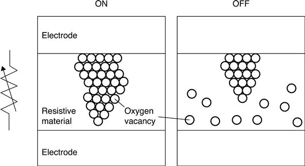
Electric field-induced resistive random access memories (RRAMs) have recently attracted a great deal of attention as promising candidates for the next generation of non-volatile memories (Akinaga and Shima 2010; Makarov et al. 2012; Nishi 2011; Sawa 2008; Waser and Aono 2007; Waser et al. 2009). The typical RRAM structure is a capacitor-like metal-insulator-metal (MIM) stack, where the resistive material is sandwiched between two metal electrodes (Fig. 8.1). The RRAM can be switched between the low resistance state (ON) and the high resistance state (OFF) of the resistive material by applying voltages to the electrodes. Recently, the successful fabrication of a 32 Gb RRAM test chip, fabricated by a 24 nm process, has been reported (Liu et al. 2013). However, a fundamental understanding of the RRAM switching mechanism, which is essential for broadening of practical RRAM applications, has not yet been obtained.
Ab initio modeling is one of the most important tools used for pursuing the fundamental aspects of RRAM switching mechanisms. Ab initio modeling provides an in-depth understanding of materials on the basis of quantum mechanics. The importance of such quantum-mechanical modeling for RRAM stems from the essential contribution made to the switching mechanism by electron motion, which crucially correlates with structural changes in the material (Nishi 2011); such atomistic structural changes result in the creation and annihilation of nanometer-scale conductive paths in the RRAM during ON-OFF switching.
In this chapter, we discuss ab initio modeling of RRAMs based on density functional theory (DFT) for investigation of the switching mechanism and to enable us to propose desirable memory structure. We focuses on roles of electronic charge in filamentary-type switching of binary oxide-based RRAMs (OxRRAMs) that have recently been drawing considerable attention, because they offer the prospect of low cost, high scalability, fast switching and low power consumption characteristics (Akinaga and Shima 2010; Nishi 2011; Makarov et al. 2012; Waser et al. 2009). Section 8.2 gives an overview of DFT-based ab initio modeling approaches for OxRRAM modeling. Sections 8.3 and 8.4 discuss application of the modeling method to OxRRAM switching to obtain not only physical concepts for comprehensive understanding of the operating mechanisms, but also extracting guiding principles for further improvement of the switching properties.
8.2 Methodology for ab initio modeling of OxRRAMs
Ab initio modeling is a methodology that is used to describe interacting electrons distributed among arrays of nuclei in materials from the first principles of quantum mechanics. It only requires specification of the constituent nuclei of the materials of interest to calculate their physical properties. Ab initio modeling thus has the power to map phenomena that cannot be simply modeled by the classical approach, in terms of electronic structures, and can thereby shed light on the role of electrons in the material (Fiolhasis et al. 2003; Kohanoff 2006; Marx and Hutter 2009; Parr and Yang 1989; Payne et al. 1992).
Ab initio modeling is based on electronic structure calculations, where the Schrödinger equation for a many-body electron system is applied to determine the electronic structures of materials. Among the variety of theoretical frameworks used to obtain solutions at different approximation levels, DFT can provide a computationally efficient approach to the modeling of systems containing hundreds of atoms, with affordable simulation times and reasonably practical accuracy levels (Fiolhasis et al. 2003; Kohanoff, 2006; Marx and Hutter 2009; Parr and Yang 1989; Payne et al. 1992) (Section 8.2.1). DFT is capable of determining a wide range of material properties that are related to the total energies, including atomistic geometries, electronic band structures and charge density distributions. In the next section, we give an overview of DFT-based ab initio modeling and the related calculation methods that are used to study OxRRAMs.
8.2.1 DFT-based ab initio modeling
DFT-based ab initio modeling provides a description of a material consisting of nuclei and electrons. It is based on non-relativistic quantum mechanics as formalized via the Schrödinger equation. In the adiabatic approximation, the motion of the electrons instantaneously follows the motion of the nuclei, and thus the nuclear co-ordinates are treated as classical variables. As a result, the equation that we must solve produces the time-independent Schrödinger equation, which is known as an electronic structure calculation (Kohanoff 2006). The electronic problem can be approached from two main types of methodology. The first is a wave-function method, such as the Hartree-Fock method, which is an approach used to obtain many-body wave functions. The second is an approach using the DFT framework, as described below.
DFT was developed by Hohenberg and Kohn (1964) and Kohn and Sham (1965). Hohenberg and Kohn (1964) proved that the total energy of an interacting electron system is given as a functional of the electron density. The density functional provides the ground-state energy of the system as a minimum value for the exact single-particle ground-state electron density. Kohn and Sham (1965) introduced an effective one-electron system in which the electron density is identical to that of the real interacting system, which leads to a variational equation (the Kohn-Sham equation) of the density functional with respect to the single-particle wave function (the Kohn-Sham orbital). Therefore, in the DFT framework, the many-body problem in an interacting electron system is formally replaced by an exactly equivalent set of self-consistent one-electron Kohn-Sham equations.
In DFT-based electronic structure calculations, the Kohn-Sham equations are solved practically using several approximations (Payne et al. 1992). Most significantly, the exchange-correlation energy, which is a purely quantum-mechanical factor, is approximated because its exact form remains undiscovered. Typical approximations include the local density approximation (LDA) (Kohn and Sham 1965) and the generalized gradient approximation (GGA) (Perdew et al. 1996). Practically, the frozen-core approximation is usually introduced to reduce the computational time dramatically. In the approximation, the electron density of the core states of material is assumed to be identical to the density of isolated atoms or ions. For implementation, the pseudo-potential is used to simulate the effects of the nucleus and the core electrons on the valence electrons. Norm-conserving pseudo-potentials (Troullier and Martins 1991), ultrasoft pseudo-potentials (Vanderbilt 1990) and the projected-augmented-wave (PAW) pseudo-potentials (Blöçhl 1994; Kresse and Joubert 1999) are frequently used in practical calculations.
The use of periodic supercells also allows us to handle an infinite number of electrons and nuclei in a material within the framework of Bloch’s theorem (Ashcroft and Mermin 1976), where the electron states can be calculated accurately by sampling special sets of k points in the Brillouin zone (Chadi and Cohan 1973; Monkhorst and Pack 1976). To expand the electronic wave functions at each k point, one of the most convenient base sets is the plane-wave base set, the completeness of which is systematically improved by an increase in the cutoff energy. The supercell approximation with the plane-wave base set is also applicable to non-periodic configurations, such as an isolated vacancy surrounded by a region of bulk crystal. In this case, a large unit cell containing the configuration of interest should be constructed to be independent of the defects in neighboring cells. For charged systems, spurious interactions between periodically repeated images should be avoided, and one of the simplest ways to do this is to add a neutralizing background charge to the system (Blöçhl 2000).
Using these approximations, the Kohn-Sham equation is then solved by an iterative technique, such as the conjugate-gradients method. The total energy of the material is calculated from the charge densities obtained. The force acting on each nucleus is obtained from the derivative of the total energy with respect to the corresponding nuclear coordinates. Using the calculated forces, the total-energy minimized atomic structures and the corresponding electronic band structures can be calculated. Combination with the molecular-dynamics technique also allows us to calculate the dynamical aspects of the systems. The DFT-based ab initio method is currently implemented in many software packages, such as VASP (2013), CPMD (2013), CASTEP (2013) and ABINIT (2013).
8.2.2 DFT-based calculation methods to study OxRRAMs
An important element in the switching mechanism of OxRRAMs is the oxygen vacancy (Akinaga and Shima 2010; Nishi 2011; Waser et al. 2009). The role of such a defect is the formation of nanoscale conductive filaments (Fig. 8.1); the formation and disruption of these filaments are the mechanisms responsible for the ON-OFF switching processes. The elementary process in filament formation/disruption is vacancy migration. For these phenomena, DFT-based ab initio modeling provides a theoretical framework to enable calculation of important quantities for the energetics, geometries and electronic structures. In this subsection, we describe some DFT-based methodologies applied to calculate these quantities.
For exchange-correlation energy functionals in the DFT-based ab initio modeling of OxRRAMs, the use of conventional LDA and GGA functionals is known to be insufficient for quantitative description of electronic structures such as the energy band gap and the positions of vacancy levels in the band gap (Gillen et al. 2012; Lee et al. 2010; Lyons et al. 2011; Magyari-Köpe et al. 2011, 2012; Park et al. 2008, 2010). This is considered to be because of a lack of self-interaction correction in these functionals, which could be necessary for transition metal oxides with well-localized d and f orbitals. One recent approach to this issue is the LDA/GGA + U method, where a Hubbard-type on-site Coulomb correction (U) is applied to the LDA/GGA functional (Anisimov et al. 1997; Kohanoff 2006); the determination of the Hubbard parameter U can be conducted by fitting it to experimental data or by estimating it from LDA/GGA-calculated total energies with varying occupancy of the localized d or f orbitals. Another approach for strongly correlated systems is the use of hybrid functionals, such as Heyd-Scuseria-Ernzerhof (HSE) or screened exchange (sX) functionals.
The energetics of the vacancies in OxRRAMs can be addressed in terms of the formation energies calculated by DFT-based ab initio methods. The formation energy of n oxygen vacancies in the charge state q, ![]() is defined as (Van de Walle and Neugebauer 2004)
is defined as (Van de Walle and Neugebauer 2004)
[8.1]
![]() is the total energy of the supercell, involving n oxygen vacancies in the charge state q, and Ebulk is the total energy of the equivalent supercell, including the bulk without vacancies. μO is the oxygen chemical potential, which represents the energy of the reservoirs with which oxygen atoms are being exchanged EF is the Fermi level with which the electrons are exchanged for the electron reservoirs, referenced to the valence-band maximum Ev in the bulk. ΔV is a correction term used to align the reference potential in the defect supercell with that in the bulk; the value of the term can be obtained from the difference in the average of the self-consistent local potential around an atom in a bulk-like environment in the defective supercell.
is the total energy of the supercell, involving n oxygen vacancies in the charge state q, and Ebulk is the total energy of the equivalent supercell, including the bulk without vacancies. μO is the oxygen chemical potential, which represents the energy of the reservoirs with which oxygen atoms are being exchanged EF is the Fermi level with which the electrons are exchanged for the electron reservoirs, referenced to the valence-band maximum Ev in the bulk. ΔV is a correction term used to align the reference potential in the defect supercell with that in the bulk; the value of the term can be obtained from the difference in the average of the self-consistent local potential around an atom in a bulk-like environment in the defective supercell.
Along with the formation energies, the vacancy cohesive energies are used to evaluate the thermodynamic stability of vacancy filaments in OxRRAMs. The cohesive energy, ![]() , of a filament comprising n oxygen vacancies in the charge state q is defined as
, of a filament comprising n oxygen vacancies in the charge state q is defined as
[8.2]
Efilament(q) is the total energy of the filament, involving n oxygen vacancies in the charge state q. Ebulk and Eisolated(q) are the total energies of the bulk in a defect-free supercell and in the system including an isolated oxygen vacancy in the charge state q, respectively; both of these quantities are calculated using the same-size supercell as that of the filamentary system. We note here that the cohesive energy can also be calculated from the difference in the formation energies between the systems involving filaments and the isolated vacancy:
[8.3]
 [8.3]
[8.3]
We note that we use the approximation that EF + Ev + ΔV is the same in the ![]() case as the
case as the ![]() case of the filament.
case of the filament.
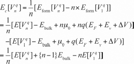
The migration process of the vacancies in OxRRAMs can be analyzed using the DFT-based ab initio calculation of the potential energy profile along the reaction pathway. On an adiabatic total energy surface in the configuration space, the diffusion path of the vacancies is described as the minimum energy path that connects the initial and final states via saddle points with the lowest activation barriers. The constrained optimization that we can use in this chapter is one of the simplest ab initio approaches for searching for the minimum energy path in the N-dimensional space, where N is the number of degrees of freedom in a supercell (Jeong and Oshiyama 1998). In this scheme (Fig. 8.2), a plane of (N − 1)-dimensional hyperspace is defined perpendicular to the line (a reaction vector) that connects the initial and final structures; geometry optimization is then performed within the (N − 1)-dimensional hyperspace using the force perpendicular to the line F|| that is defined as
[8.4]
where F is the force acting on the nuclei (an N-dimensional vector; F = (F1, …, FM, where Fi is the force acting on the i-th nucleus and M is the total number of nuclei) and h is the normalized N-dimensional vector along the reaction vector. The constraint optimization approach thus converts the problem of searching for the minimum energy path in the N-dimensional space into a structural optimization problem with a constraint in (N − 1)-dimensional space. The advantage of using this method is that we can perform the constraint optimization independently of all of the geometries that are initially located at different positions on the reaction vector, which reduces the computational time dramatically. However, for more accurate determination of the saddle point, it is necessary to use other methods, such as calculation of the Hessian matrix, with higher computational costs. In addition, for more accurate analysis of the reaction pathway, it is necessary to use more sophisticated methods, such as the nudged elastic band method (Henkelman et al. 2000).
8.3 Physical concept for OxRRAM switching mechanisms based on density functional theory (DFT)-based ab initio modeling
DFT-based ab initio modeling of RRAMs has been performed over the past few years, which has focused mainly on the role of defects, and in particular oxygen vacancies, in resistive switching. In the previous studies, this quantum-mechanical modeling has clarified the modulation of the electronic structure atomistically in terms of the existence of vacancies in SrTiO3-based RRAMs (Jeon et al. 2006; Szot et al. 2006; Wang et al. 2009; Waser et al. 2009). In recent years, ab initio modeling of the conductive filaments composed of oxygen vacancies in OxRRAMs has become a topic of considerable interest (Kamiya et al. 2012a,b, 2013a,b; Lee et al. 2010; Magyari-Köpe et al. 2011, 2012; Park et al. 2011a,b; Yang et al. 2013a,b), stimulated by the direct observation of nanoscale filaments by high-resolution transmission electron microscopy in TiO2-based RRAMs (Kwon et al. 2010; Strachan et al. 2010). These simulations have shown their ability to describe the atomistic and electronic structures of the conductive filaments, thereby proving their power to address the ON-OFF switching mechanisms in terms of filament formation and disruption by vacancy migration.
In this section, we discuss the mechanisms of filament formation and disruption in OxRRAMs based on DFT-based ab initio calculations. The energetics and electronic structures of the vacancy filaments are analysed to determine the essential electronic factors that contribute to the filament formation. The physical concept for the filamentary switching mechanism is then derived based on the calculated results.


8.3.1 Energetics and electronic structures of oxygen vacancy filaments in OxRRAMs
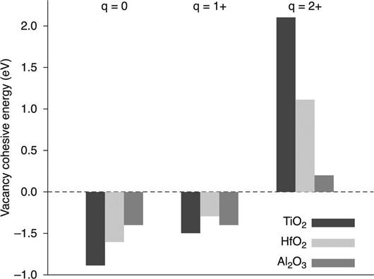
We first discuss the energetics of filament formation in TiO2, HfO2 and Al2O3 (Kamiya et al. 2012a,b2013a,b; Yang et al. 2013a,b). The filament models, including the ordered oxygen vacancies, are shown in Fig. 8.3. These models correspond to the conductive ‘ON’ state of memory operation. The vacancy filament formation energetics in these binary oxides are then investigated by calculating the cohesive energy (Section 8.2.2) for the filament models. The calculated cohesive energy is shown in Fig. 8.4 for filament formation in TiO2, HfO2 and Al2O3. There is a strong dependence of the average charge per vacancy on the cohesive energy: for all oxides, the cohesive energy is less than zero when the vacancies take neutral or singly positive charge states, while it is greater than zero for doubly positive charged vacancies. This clearly indicates the inherent nature of the vacancy cohesion-isolation induced by charge injection/removal in the binary oxides, i.e. isolated oxygen vacancies take a doubly positive charge state, but when they capture electrons, the vacancies then tend to be clustered. These results strongly suggest that the energetics of vacancy cohesion-isolation in OxRRAMs are generally determined by charge injection/removal.

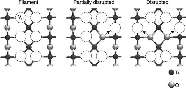
More detailed analysis of the energetics of filament formation-disruption has been performed on TiO2 (Kamiya et al. 2012a,b, 2013a,b; Magyari-Köpe et al. 2011, 2012; Park et al. 2011a,b). In addition to the filament model with a vacancy-ordered configuration, the disrupted filament model shown in Fig. 8.5 is also considered. Analysis of the partial charge densities has shown that the conductive channel is ruptured in this model, thereby corresponding to the ‘OFF’ state of memory operation (Kamiya et al. 2013b). The thermodynamic stability of the two models is then investigated by calculating the vacancy formation energy (Section 8.2.2). The calculated formation energy is plotted in Fig. 8.6 as a function of the Fermi energy, which is also shown in the isolated vacancy case. In the isolated situation, the vacancies take a doubly positive charge state for almost the entire Fermi energy range.
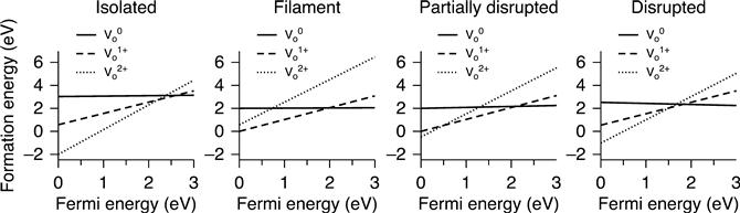
In contrast, when the vacancies form an ordered filament, the energetically favourable average charge per vacancy is neutral or singly positive for the whole Fermi energy range. However, this trend is changed by filament disruption; the doubly positive charge becomes the most stable charge state for a wide Fermi energy range. These results suggest that the filament formation-disruption energetics in OxRRAMs are determined by charge injection/removal, which can be changed through a shift in the Fermi energy under an applied voltage during memory operation.
Further atomistic investigation of the filament formation-disruption transition in TiO2-based RRAMs also clarifies the importance of charge injection/removal effects on the energetics (Kamiya et al. 2012a,b). The elementary reaction of filament formation-disruption is the vacancy migration. In the case of the filament-and disrupted-filament models described above, the elementary step is a single-step jump of a single vacancy to the outside of the filament. The potential energy profile for this vacancy diffusion is then investigated by the constraint optimization method (Section 8.2.2). The calculated profiles for vacancies with singly positive or doubly positive average charges are shown in Fig. 8.7. When the vacancies take a singly positive charge state, the filamentary state is more stable than the disrupted state by approximately 2 eV. This stabilization leads to the formation of a high energy barrier for vacancy diffusion.

In sharp contrast, the filamentary state is much less stable, by about 4 eV when the vacancies have a doubly positive charge state, which eventually lowers the vacancy diffusion barrier by as much as 0.6 to 0.7 eV. In this situation, the vacancy migration process can be activated by sufficient thermal energy provided by Joule heating. These results indicate that charge injection/removal determines the overall energetics of the filament formation/disruption transition in OxRRAMs, where electron removal makes the energy barrier of the vacancy diffusion processes small enough to be overcome by Joule heating.
Detailed investigation of the electronic structure of vacancy filaments in OxRRAMs is important for a full understanding of the filament formation/disruption mechanism induced by vacancy cohesion-isolation upon charge injection/removal (Kamiya et al. 2012a,b; Magyari-Köpe et al. 2011, 2012; Park et al. 2011a,b). Figure 8.8 shows the electronic energy bands and the density of states (DOS) of a filament-formed model and a filament-disrupted model in TiO2 for optimal charge states. The energy band structures of the doubly positive isolated vacancy in TiO2 are also shown in the same figure. In the isolated case, the defect level is located just below the bottom of the conduction band. This indicates that the occupation of this defect state needs a high Fermi energy measured from the top of the valence band. Therefore, an isolated vacancy with a doubly positive charge is stable over a large Fermi energy range (Fig. 8.6). It is also found that the defect level has no dispersion; the corresponding wave function is highly localized, and is characterized by the d orbitals of three local Ti ions close to the vacancy site (Park et al. 2010).
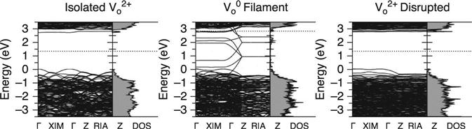
These electronic features change dramatically when the oxygen vacancies form a cohesive filament. As shown in Fig. 8.8, the defect levels form a band with significant dispersion only along the Γ to Z line in k space, which corresponds to the [001] direction (the vacancy-ordered direction) in real space. The corresponding wave functions are delocalized along the [001] direction (Kamiya et al. 2013b). They are also characterized by bonding-like and antibonding-like orbitals. As a result of the occupation of the bonding-like states, singly positive and neutral charge states appear as stable states for the whole Fermi energy range (Fig. 8.6). However, when the filament is disrupted by vacancy migration, this large band dispersion disappears (Fig. 8.8); the corresponding wave functions then have localized, disconnected characteristics (Kamiya et al. 2013b). Consequently, the doubly positive charge state becomes the most stable state in a wide Fermi energy range (Fig. 8.6). Very similar results were found for filament formation in HfO2 (Kamiya et al. 2013a) and in Al2O3 (Yang et al. 2013a).
8.3.2 Physics of filament formation and disruption in OxRRAMs
As a physical effect of the applied electric field on filament formation/disruption in OxRRAMs, the drift of positively charged vacancies has been considered over the past few years (Gao et al. 2011; Ielmini 2011; Nardi et al. 2012; Yu et al. 2011). In contrast, as discussed in the previous subsection, the DFT-based ab initio calculations highlight another critical effect on filament formation/disruption, i.e. the electric field-induced charge injection/removal process that determines the thermodynamic stability of the vacancy filament. The importance of this effect in OxRRAM switching can be understood through a comparison between the cohesive energy provided by charge injection-induced vacancy interactions and the typical energy provided by the applied voltages. As shown in Fig. 8.4, the calculated cohesive energy gain is of the order of 1 eV per single vacancy in binary oxides (Kamiya et al. 2012b, 2013a,b; Yang et al. 2013a). This value is comparable to the energy gain provided by a typical voltage of approximately 1 V when applied during memory operation.
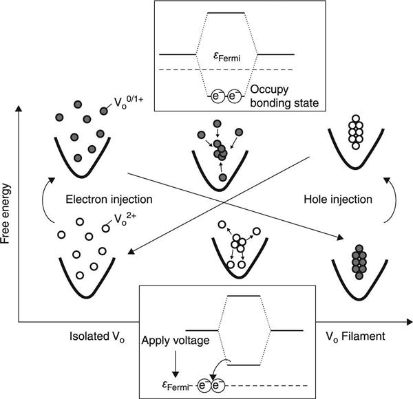
Charge injection/removal by the applied electric field induces the vacancy cohesion-isolation. The most important physical process here is the formation of bonding-like electron states and the control of the occupation of these states by applying voltages (Fig. 8.9). When the vacancies come close to one another, quantum mechanical interactions between their defect levels lead to bonding-like and antibonding-like electron states. The bonding-like orbitals are occupied by electrons that are injected by an upward shift in the Fermi energy induced by the applied voltages. This process provides an energy gain for the electronic system, which leads to vacancy cohesion. In contrast, the electrons can be removed from these bonding-like states by a downward shift in the Fermi energy induced by the applied voltages, which enhances the vacancy isolation.
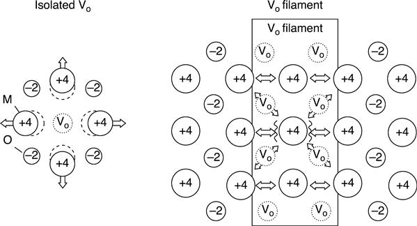
In addition to bonding-state formation, Coulomb repulsion between the metal ions in the binary oxides is another competing factor in determination of the energetics of filament formation/disruption. In the case of an isolated vacancy with a doubly positive charge, positively charged metal ions such as Ti4+ and Hf4+ move outward to reduce the strong Coulomb repulsion between the ions, which leads to stabilization of the vacancy charge state (Fig. 8.10). In contrast, when the vacancies form a cohesive filament, this outward displacement of the metal ions is strongly suppressed because of the geometrical restrictions of the filamentary structure (Fig. 8.10). Therefore, the electrons should be incorporated into the filament to reduce the Coulomb repulsion between the metal ions. In addition to this neutralization effect, electron injection leads to further stabilization of the electron systems by occupation of the bonding states, as described above. These two stabilization effects compete with each other, and this determines the number of electrons injected into the vacancy filament. Complete neutralization by injection of an equal number of electrons per vacancy results in the maximum reduction in the Coulomb repulsion between the metal ions, but the electronic effect is small, because the injected electrons occupy not only the bonding-like states but also the antibonding-like states. In contrast, partial neutralization leads to high electron energy gain caused by decreasing occupation of the antibonding-like states, but the Coulomb repulsion between the metal ions is high. These considerations suggest that the energetically favourable charge state of the vacancy filament has site dependence; vacancies inside a thick filament are expected to preferentially take a neutral charge state because of the large degree of geometrical restriction, while vacancies in a thin filament or located near the interface between the filamentary region and the host crystal can take a positively charged state because the geometrical restrictions are smaller.
The cohesion-isolation of the oxygen vacancies caused by charge injection/removal eventually induces a phase transition accompanied by vacancy collective motions (Kamiya et al. 2012b, 2013b). The cohesive transition between isolated and ordered vacancies is driven to gain high cohesive energy when electrons are injected into the isolated vacancies with doubly positive charges. In contrast, when holes are injected into the filament, the isolation transition is caused by strong Coulomb repulsion between vacancies with doubly positive charges.
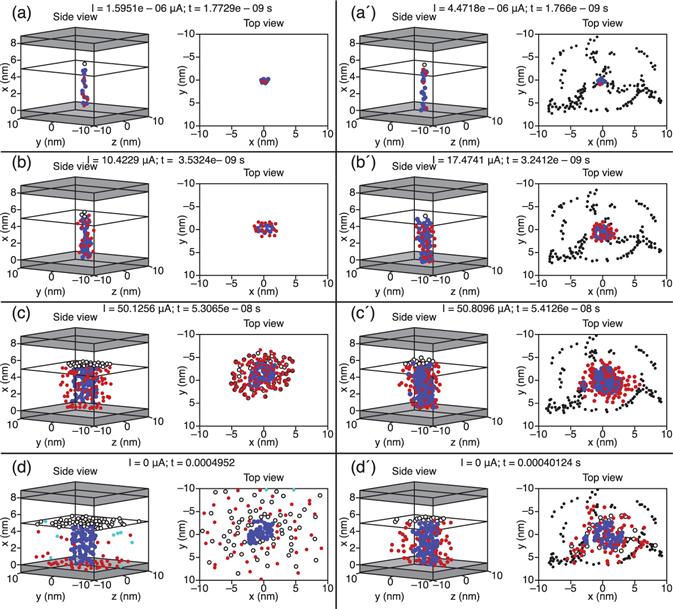
The vacancy cohesion-isolation phase transition upon charge injection/removal under an applied voltage can change the filament formation-disruption dynamics in the OxRRAM from a stochastic nature into a deterministic nature. Quantum mechanics-based Monte Carlo simulations that include such phase transitions have demonstrated deterministic formation of pyramidal-shaped filaments when electrons are injected from the filament to the isolated vacancies with doubly positive charges; reversing the voltage leads to electron removal from the neutral vacancies, which causes a repulsive Coulomb explosion between the charged vacancies at the top of the filament. Thus, the structural change of the filament formation-disruption process is essentially reversible, which originates from the vacancy cohesion-isolation phase transition upon charge injection/removal.
Based on the above ab initio analyses, we conclude that the vacancy cohesion-isolation phase transition upon charge injection/removal is one of the main physical processes of filament formation-disruption in OxRRAMs. This physical concept is universal, regardless of the type of binary oxides involved, because it is related to vacancy-inherent properties. This enables us to provide universal guiding principles for high-quality OxRRAMs, which are discussed in the next section.
8.4 OxRRAM optimization based on DFT-based ab initio modeling
The physical concept revealed by DFT-based ab initio modeling of OxRRAMs in the previous section is that the vacancy cohesion-isolation phase transition upon charge injection/removal is one of the main factors governing the ON-OFF process. This strongly suggests that proper control of such phase transitions is crucial for OxRRAM optimization to improve the memory properties. Recent experiments have shown that using a stacked OxRRAM structure is one of the most promising methods to improve the memory characteristics, such as the ON/OFF ratio (Chien et al. 2012; Goux et al. 2012; Kim et al. 2012; Lee et al. 2012). In this section, we discuss guidelines for design of the most favourable stack structure in terms of control of the vacancy phase transition to further improve OxRRAM memory properties such as the ON/OFF ratio and the program/erase cycles endurance. A case study of a TiN/Al2O3/HfO2/Hf/TiN RRAM stack is also included.
8.4.1 Oxygen chemical potential modulation in three-layer stacked OxRRAM
Two variables control the vacancy cohesion-isolation phase transition in OxRRAMs; the vacancy charge state and the oxygen chemical potential. This can be understood by considering the vacancy formation energy, which is a strong driving force for the cohesion-isolation phase transition. The formula for the formation energy (Section 8.2.2) indicates the dependencies of the vacancy charge state, the system Fermi energy and the oxygen chemical potential. The charge state and the system Fermi energy can be controlled by injection/removal of charges and application of a voltage, while the O chemical potential can be tuned by stacking engineering.
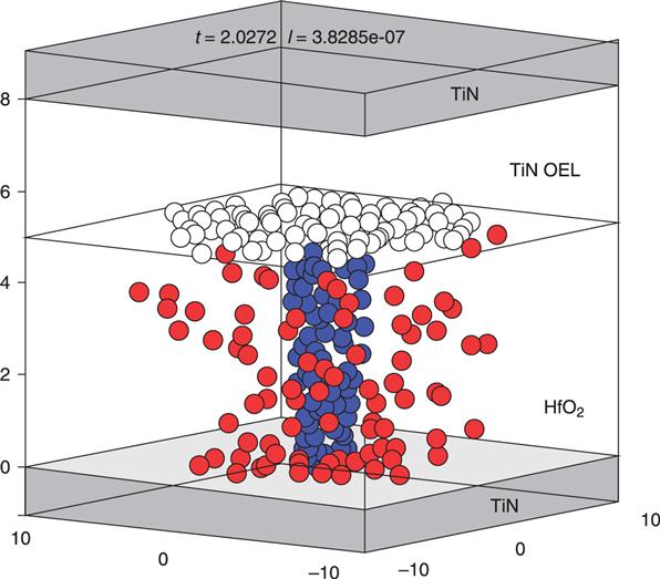
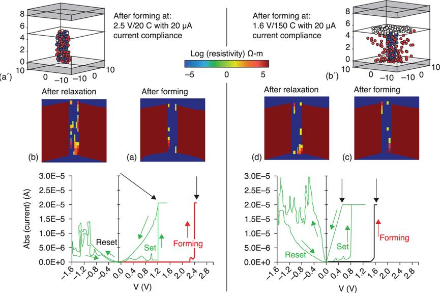
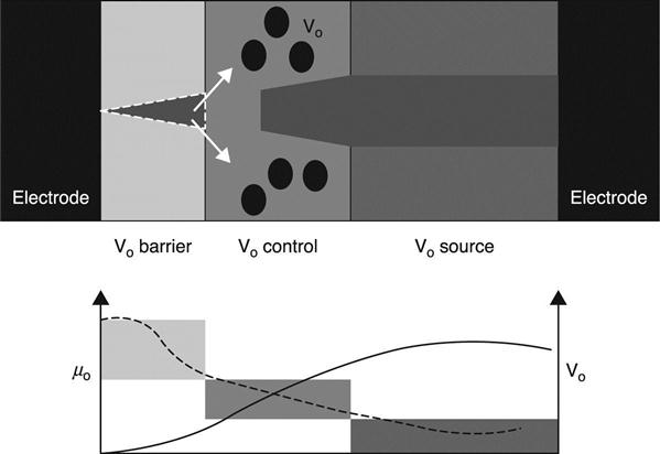
One of the most promising candidates for the OxRRAM stack is a three-layer structure composed of a vacancy-source layer, a vacancy-control layer and a vacancy-barrier layer (Fig. 8.11). The vacancy-source layer has a high vacancy concentration, and thus its oxygen chemical potential is low. In sharp contrast, the vacancy-barrier layer has a low vacancy concentration and high O chemical potential. Stacking of these layers therefore produces spatial differences in the O chemical potential in the OxRRAM cell, which leads to an asymmetrical vacancy filament shape that can be used to improve the memory characteristics. Figure 8.11 shows that such filaments can be disrupted completely in the vacancy-barrier layer in the OFF state, which contributes to the high resistance ON/OFF ratio; this has actually been demonstrated in a TiN/Al2O3/HfO2/Hf/TiN OxRRAM stack (Goux et al. 2012).
The ON-OFF switching mechanism in the three-layer stack structure has been proposed based on the DFT-based ab initio calculations (Fig. 8.12) (Kamiya et al. 2012b, 2013b; Yang et al. 2013a). In the reset switching process (from ON to OFF), the electrons are removed around the interfaces between the vacancy-barrier and vacancy-control layers, because there is a local electric field concentration that sensitively depends on the asymmetrical shape of the filament (Fig. 8.12(b)). At the same time, Joule heating provides sufficient thermal energy to trigger the migration of vacancies with doubly positive charges. This process leads to the vacancy cohesion-isolation phase transition, which disrupts the vacancy filament near the vacancy-barrier/control layers (Fig. 8.12(c)). As a result of this filament disruption, the vacancy-barrier layer has a high O chemical potential with high system Fermi energy (negative bias near the layer). This causes a complete release of the vacancy from the barrier layer to the vacancy-control layer (Fig. 8.12(d)), which eventually leads to the OFF state (Fig. 8.12(e)).
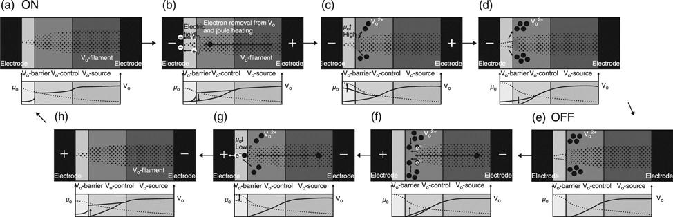
In the set process (from OFF to ON), the electrons are injected from the top of the filament into isolated vacancies with doubly positive charges (Fig. 8.12(f)). Vacancies with neutral or singly positive charges then cohere via the vacancy cohesion-isolation phase transition, which leads to filament growth in the vacancy-control layer. As a result of this filament formation, the vacancy-barrier layer has a low O chemical potential with low system Fermi energy (positive bias near the layer) (Fig. 8.12(g)). This leads to vacancy migration from the vacancy-control layer to the vacancy-barrier layer and further vacancy filament growth (Fig. 8.12(h)), which finally leads to the ON state (Fig. 8.12(a)).
8.4.2 Desired structure for three-layer stacked OxRRAM
The proposed ON/OFF mechanism strongly suggests that the desired three-layer stack structure consists of:
1. a vacancy-source layer with an extraordinarily low O chemical potential;
2. a vacancy-control layer with a thickness that is thinner than the penetration depth of the O chemical potential; and
3. a vacancy-barrier layer with a thickness that is thinner than the direct electron tunnelling.
It is necessary to use these sources and control layers to inject vacancies into the vacancy-barrier layer, where the O chemical potential is intrinsically very high. In practice, the optimization of the vacancy-source layer can be performed by selecting highly reactive transition metals or metal rich oxides, while the vacancy-control layer can be optimized by thinning it to a thickness of less than about 5 nm, which is the typical vacancy diffusion length (O chemical penetration depth).
As far as the desirable vacancy-barrier layer is concerned, thicknesses of less than the typical electron direct-tunnelling length are necessary to produce a large energy gain for electronic systems, as suggested by the following filament growth mechanism (Fig. 8.13). Let us consider bipolar operation, which leads to ON-OFF switching by applying voltages in opposite directions (Fig. 8.13(a)). The vacancy defect levels in the vacancy-barrier layer (Edefect) are assumed to be located at a lower energy than the Fermi level of the vacancy filament. If a positive voltage (+V) is applied to the electrode next to the barrier layer, then the Fermi level of the electrode (EelectrodeF) can be then reduced such that it is lower than the vacancy defect levels. In this case, electron transfer from a vacancy to the electrode via direct tunnelling can at least provide an energy gain of 2 × (V − (EelectrodeF − Edefect)) per pair of electrons. In addition to this energy gain, the vacancy cohesion at the top of the filament can also provide an energy gain (Ecohesive). As a result, the total energy gain for the entire process is at least Egain = 2 × (V − (EelectrodeF − Edefect)) + Ecohesive. However, the energy cost (Ecost) can be estimated by considering the reduction reaction of the vacancy-barrier layer by the vacancy-control layer; therefore satisfying the condition where |Egain| ≥ |Ecost| leads to filament growth in the vacancy-barrier layer.

A similar mechanism is possible for unipolar operations of the three-layer-OxRRAM (Fig. 8.13(b) (Yang et al. 2013a)). Unipolar operation leads to ON-OFF switching by application of a voltage, and depends not on its polarity but on its strength. If a negative bias (−V) is applied to an electrode, the positions of the defect levels in the vacancy-barrier layer can be raised. Electron transfer from the vacancy to the Fermi level of the filament (EfilamentF) via direct tunnelling can provide an energy gain of at least Egain = 2 × (V-(EfilamentF − Edefect)) per two electrons. Therefore, satisfaction of the condition of |Egain| ≥ |Ecost| is possible under a high voltage in the same polarity, which leads to filament growth in the vacancy-barrier layer.
It is notable that during bipolar operation, the vacancies in the barrier layer are likely to be located near the top of the filament rather than at the positively biased electrode. This is because:
1. the vacancies incorporated from the vacancy-control layer tend to be doubly positive; and
2. the O chemical potential in the barrier layer is lower near the control layer side than at the electrode side because of stacking (Fig. 8.13).
In contrast, doubly positive vacancies in the barrier layer tend to be formed near the negatively biased electrode during unipolar operation; the electrons are then injected into the vacancies from the electrode, which leads to filament formation in different directions, unlike the bipolar case. In each case, electron transfer is the main driving force behind vacancy formation in the vacancy-barrier layer. Therefore, the barrier layer thickness should be less than the distance that allows direct electron tunnelling through the layer, which is typically about 2 nm. Furthermore, from the viewpoint of the electronic properties, such as band offsets and the positions of the defect levels, appropriate material selection for the vacancy-barrier layer with respect to the vacancy-control/source layers and the electrodes is also important to maximize the electronic effect.
Consider the optimization of the stacked OxRRAM from some different viewpoints. As discussed in Section 8.3.2, the vacancy cohesion-isolation phase transition induced by the charge injection/removal results in the nearly reversible formation of pyramidal filaments in the OxRRAM. This contributes to improvements in the program/erase cycles, as also noted in other types of non-volatile memory (Kamiya et al. 2011; Yamaguchi et al. 2010, 2011). In addition, the formation of the pyramidal-shaped filament may improve the data retention properties. Therefore, maximizing the electronic effects in OxRRAMs by optimizing the stack structures and selecting the appropriate oxides and electrode materials is expected to improve the memory characteristics, including high program/erase cycles endurance and high ON/OFF ratio. However, further detailed analysis is necessary.
8.4.3 A case study of the TiN/Al2O3/HfO2/Hf/TiN RRAM stack
In practice, Al2O3 is one of the most promising vacancy-barrier layers. This is because:
1. it is an O interstitial former; and
2. its defect level is lower than that of conventional OxRRAM oxide layers, such as TiO2 (Park S.-G. 2010; Robertson 2000), HfO2 (Gillen 2012; Robertson 2000), Ta2O5 (Ramprasad 2003; Robertson 2000) and W O3 (Wang et al. 2011, 2012), and comparable to the Fermi levels of typical electrode materials such as TiN and W.
SiO2 is a possible candidate vacancy-barrier layer material, but its defect level is too low when compared with the Fermi levels of the typical electrode materials TiN and W (Oshiyama 1998), which suggests that it requires high switching voltages.
Here, we apply the above discussion to the case of the TiN/HfO2/Hf/TiN OxRRAM stack with an Al2O3 barrier layer (Kamiya et al. 2012b; Yang et al. 2013a). If we consider the reduction reaction of Al2O3 by the reactive Hf layer, then the formation of the oxygen vacancy in Al2O3 is an endothermic reaction, which requires an energy of 8.0 eV according to ab initio calculations (Yang et al. 2013a):
[8.5]
However, the oxidation of Hf is an exothermic reaction, which gives an energy of 5.8 eV calculated from the heart of formation (Samsonov 1981):
[8.6]
Therefore, the total reaction is an endothormic reaction, which requires an energy of Ecost = 2.2 eV:
[8.7]
In contrast, the energy gain Egain in the OxRRAM stack structure during bipolar operation is evaluated as follows (Fig. 8.13). The vacancy defect levels in the Al2O3 layer, Edefect, are calculated to be 4.0 eV from the valence band top (Yang 2013a). Assuming the use of a TiN electrode, the work function is approximately 4.9 eV; the Fermi level of the electrode EelectrodeF is thus calculated to be 4.0 eV from the top of the Al2O3 valence band (Miyazaki 2001; Yang et al. 2013a). By applying a positive voltage of 1.0 V to the electrode, the energy gain generated by the direct two-electron transfer from the vacancy to the electrode is estimated to be at least 2 × (V − (EelectrodeF − Edefect)) = 2 × (1.0 − (4.0 − 4.0)) = 2.0 eV. However, the cohesive energy of the vacancy, Ecohesive, is about 0.4 eV (Fig. 8.4). Therefore, the total energy gain for the overall process is at least Egain = 2.0 eV + 0.4 eV = 2.4 eV. This satisfies the critical condition of |Egain| > |Ecost| = 2.2 eV. Therefore, applying a voltage of approximately 1 V provides a large enough energy gain to overcome the energy cost, which eventually leads to filament growth in the Al2O3 barrier layer. Similarly, for the unipolar operation case, the energy gain can be estimated by the use of Egain = 2 × (V − (EfilamentF − Edefect)). Assuming EfilamentF to be 5.5 eV, which is estimated from the vacancy level in HfO2 measured from the top of the Al2O3 valence band (Robertson 2000; Gillen et al. 2012), applying a voltage of −2.7 V can provide an energy of 2 × (2.7 − (5.5 − 4.0)) = 2.4 eV, which satisfies the critical condition for filament growth in the vacancy-barrier layer. It should be noted that the present mechanism suggests that the voltages for the set process in the unipolar operation are more than two times higher.
8.5 Conclusion and future trends
This chapter has discussed the ab initio modeling of RRAM based on density functional theory for investigation of the switching mechanisms and proposal of desirable memory structures. Emphasis has been placed on the electronic roles in the filamentary-type switching of binary oxide-based RRAMs. We have demonstrated the cohesion-isolation nature of the vacancy, depending on the charge states, which is inherent in binary oxides. Because of this nature, charge injection and removal determine the thermodynamic stability of the vacancy filament and the diffusion in binary-oxide-based RRAMs; injection of electrons induces the vacancy cohesion that stabilizes the filament, whereas removal of the electrons favors the vacancy isolation that destabilizes the filament. However, electron removal makes the energy barrier of the vacancy diffusion processes small enough to be overcome by Joule heating. The physical mechanism of vacancy cohesion-isolation upon charge injection/removal is the formation of bonding-like electron states between the vacancies. The charge injection and removal that lead to occupation of the bonding-like states can be controlled by shifting of the system Fermi level via an applied voltage during memory operation. We have then derived the physical concept where the vacancy cohesion-isolation phase transition upon charge injection/removal is one of the main factors that governs the switching processes of binary oxide based RRAMs.
Based on the physical concept obtained from the ab initio calculations, the discussion has focused on the optimization of binary-oxide-based RRAM stack structures. The oxygen chemical potential has been shown to be a key parameter in stacking engineering. We have proposed an ON-OFF switching mechanism in a three-layer stack structure, which requires proper tuning of both the oxygen chemical potential and the charge injection/removal. The desired structure of the three-layer RRAM consists of:
1. a vacancy-source layer with an extraordinarily low O chemical potential;
2. a vacancy-control layer with a thickness that is thinner than the penetration depth of the O chemical potential; and
3. a vacancy-barrier layer with a thickness that is thinner than the direct electron tunneling.
Optimization of the stack structures has also been discussed in terms of the reversibility of filament formation caused by the vacancy cohesion-isolation upon charge injection/removal. The guiding principles have been applied to the optimization of the TiN/Al2O3/HfO2/Hf/TiN RRAM stack.
Finally, we comment on future trends in ab initio modeling of RRAM. The ab initio modeling of RRAM is a bottom-up approach with the aim of understanding the operating mechanism from processes at the atomistic scale, i.e. the angstroms size-scale and the femtoseconds time-scale. Derivation of physical concepts from the obtained microscopic information is important for disentanglement of complex processes and discerning the relevant and dominant factors for the RRAM switching. These concepts would also provide important information for the complementary use of macroscopic modeling methods, such as Monte Carlo simulations. Therefore, the ab initio modeling contributes significantly to clarification of the connection of the atomistic-scale phenomena to the macroscopic behaviour during RRAM operation, which is necessary to gain systematic and comprehensive understanding of the operating mechanisms. This eventually leads to estimation of the reliability, endurance, retention or scaling limits of the RRAM devices.