
Chapter 7. Preamplifiers and Input Signals
7.1. Requirements
Most high-quality audio systems are required to operate from a variety of signal inputs, including radio tuners, cassette or reel-to-reel tape recorders, compact disc players, and more traditional record player systems. It is unlikely at the present time that there will be much agreement between the suppliers of these ancillary units on the standards of output impedance or signal voltage that their equipment should offer.
Except where a manufacturer has assembled a group of such units, for which the interconnections are custom designed and there is in-house agreement on signal and impedance levels—and, sadly, such ready-made groupings of units seldom offer the highest overall sound quality available at any given time—both the designer and the user of the power amplifier are confronted with the need to ensure that their system is capable of working satisfactorily from all of these likely inputs.
For this reason, it is conventional practice to interpose a versatile preamplifier unit between the power amplifier and the external signal sources to perform the input signal switching and signal level adjustment functions.
This preamplifier either forms an integral part of the main power amplifier unit or, as is more common with the higher quality units, is a free-standing, separately powered unit.
7.2. Signal Voltage and Impedance Levels
Many different conventions exist for the output impedances and signal levels given by ancillary units. For tuners and cassette recorders, the output is either that of the German Deutsches Industrie Normal (DIN) standard, in which the unit is designed as a current source, which gives an output voltage of 1 mV for each 1000 ohms of load impedance, such that a unit with a 100-K input impedance would see an input signal voltage of 100 mV, or the line output standard, designed to drive a load of 600 ohms or greater, at a mean signal level of 0.775 V rms, often referred to in tape recorder terminology as OVU.
Generally, but not invariably, units having DIN type interconnections, of the styles shown in Figure 7.1, will conform to the DIN signal and impedance level convention, whereas those having “phono” plug/socket outputs, of the form shown in Figure 7.2, will not. In this case, the permissible minimum load impedance will be within the range 600 to 10,000 ohms, and the mean output signal level will commonly be within the range 0.25–1 V rms.
Figure 7.1. Common DIN connector configurations.

Figure 7.2. The phono connector.

An exception to this exists regarding compact disc players, where the output level is most commonly 2 V rms.
7.3. Gramophone Pick-Up Inputs
Three broad categories of pick-up (PU) cartridges exist: the ceramic, the moving magnet or variable reluctance, and the moving coil. Each of these has different output characteristics and load requirements.
7.3.1. Ceramic Piezo-Electric Cartridges
These units operate by causing the movement of the stylus due to groove modulation to flex a resiliently mounted strip of piezo-electric ceramic, which then causes an electrical voltage to be developed across metallic contacts bonded to the surface of the strip. They are commonly found only on low-cost units and have a relatively high output signal level, in the range 100–200 mV at 1 kHz.
Generally, the electromechanical characteristics of these cartridges are tailored so that they give a fairly flat frequency response, although with some unavoidable loss of HF response beyond 2 kHz, when fed into a preamplifier input load of 47,000 ohms.
Neither the HF response nor the tracking characteristics of ceramic cartridges are particularly good, although circuitry has been designed with the specific aim of optimizing the performance obtainable from these units.[1] However, in recent years, the continuing development of PU cartridges has resulted in a substantial fall in the price of the less exotic moving magnet or variable reluctance types so that it no longer makes economic sense to use ceramic cartridges, except where their low cost and robust nature are of importance.
7.3.2. Moving Magnet and Variable Reluctance Cartridges
These are substantially identical in their performance characteristics and are designed to operate into a 47-K load impedance, in parallel with some 200–500 pF of anticipated lead capacitance. Since it is probable that the actual capacitance of the connecting leads will only be of the order of 50–100 pF, some additional input capacitance, connected across the phono input socket, is customary. This also will help reduce the probability of unwanted radio signal breakthrough.
PU cartridges of this type will give an output voltage that increases with frequency in the manner shown in Figure 7.3(a), following the velocity characteristics to which LP records are produced, in conformity with the Recording Industry Association of America (RIAA) recording standards. The preamplifier will then be required to have a gain/frequency characteristic of the form shown in Figure 7.3(b), with the deemphasis time constants of 3180, 318, and 75 μs, as indicated in the figure.
Figure 7.3. The RIAA record/replay characteristics used for 33/45 rpm vinyl discs.

The output levels produced by such PU cartridges will be of the order of 0.8–2 mV/cm/s of groove modulation velocity, giving typical mean outputs in the range of 3–10 mV at 1 kHz.
7.3.3. Moving Coil Pick-Up Cartridges
These low-impedance, low-output PU cartridges have been manufactured and used without particular comment for very many years. They have come into considerable prominence in the past decade because of their superior transient characteristics and dynamic range as the choice of those audiophiles who seek the ultimate in sound quality, even though their tracking characteristics are often less good than is normal for MM and variable reluctance types.
Typical signal output levels from these cartridges will be in the range 0.02–0.2 mV/cm/s into a 50- to 75-ohm load impedance. Normally, a very low-noise head amplifier circuit will be required to increase this signal voltage to a level acceptable at the input of the RIAA equalization circuitry, although some of the high output types will be capable of operating directly into the high-level RIAA input. Such cartridges will generally be designed to operate with a 47-K load impedance.
7.4. Input Circuitry
Most of the inputs to the preamplifier will merely require appropriate amplification and impedance transformation to match the signal and impedance levels of the source to those required at the input of the power amplifier. However, the necessary equalization of the input frequency response from a moving magnet, moving coil, or variable reluctance PU cartridge, when replaying an RIAA preemphasized vinyl disc, requires special frequency shaping networks.
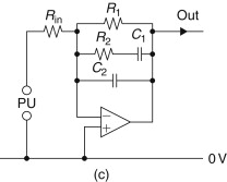
Various circuit layouts have been employed in the preamplifier to generate the required “RIAA” replay curve for velocity sensitive PU transducers, and these are shown in Figure 7.4. Of these circuits, the two simplest are the “passive” equalization networks shown in Figures 7.4(a) and 7.4(b), although for accuracy in frequency response they require that the source impedance is very low and that the load impedance is very high in relation to R1.
Figure 7.4. Circuit layouts that will generate the type of frequency response required for RIAA input equalization.


The required component values for these networks have been derived by Livy[2] in terms of RC time constants and set out in a more easily applicable form by Baxandall[3] in his analysis of the various possible equalization circuit arrangements.
From the equations quoted, the component values required for use in the circuits of Figures 7.4(a) and 7.4(c) would be
![]() For the circuit layouts shown in Figures 7.4(b) and 7.4(d), the component values can be derived from the relationships:
For the circuit layouts shown in Figures 7.4(b) and 7.4(d), the component values can be derived from the relationships:
The circuit arrangements shown in Figures 7.4(c) and 7.4(d) use “shunt” type negative feedback (i.e., that type in which the negative feedback signal is applied to the amplifier in parallel with the input signal) connected around an internal gain block.
These layouts do not suffer from the same limitations with respect to source or load as the simple passive equalization systems of Figures 7.4(a) and 7.4(b). However, they do have the practical snag that the value of Rin will be determined by the required PU input load resistor (usually 47k for a typical moving magnet or variable reluctance type of PU cartridge), and this sets an input “resistor noise” threshold, which is higher than desirable, as well as requiting inconveniently high values for R1 and R2.
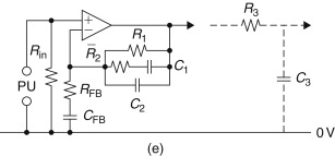
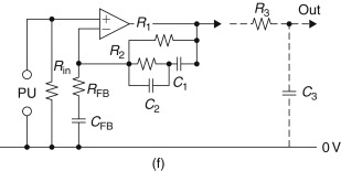
For these reasons, the circuit arrangements shown in Figures 7.4(e) and 7.4(f) are found much more commonly in commercial audio circuitry. In these layouts, the frequency response shaping components are contained within a “series” type feedback network (i.e., one in which the negative feedback signal is connected to the amplifier in series with the input signal), which means that the input circuit impedance seen by the amplifier is essentially that of the PU coil alone and allows a lower midrange “thermal noise” background level.
The snag, in this case, is that at very high frequencies, where the impedance of the frequency-shaping feedback network is small in relation to RFB, the circuit gain approaches unity, whereas both the RIAA specification and the accurate reproduction of transient waveforms require that the gain should asymptote to zero at higher audio frequencies.
This error in the shape of the upper half of the response curve can be remedied by the addition of a further CR network, C3/R3, on the output of the equalization circuit, as shown in Figures 7.4(e) and 7.4(f). This amendment is sometimes found in the circuit designs used by the more perfectionist of the audio amplifier manufacturers.
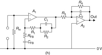
Other approaches to the problem of combining low input noise levels with accurate replay equalization are to divide the equalization circuit into two parts, in which the first part, which can be based on a low noise series feedback layout, is only required to shape the 20-Hz to 1-kHz section of the response curve. This can then be followed by either a simple passive RC roll-off network, as shown in Figure 7.4(g), or by some other circuit arrangement having a similar effect, such as that based on the use of a shunt feedback connected around an inverting amplifier stage, as shown in Figure 7.4(h), to generate that part of the response curve lying between 1 kHz and 20 kHz.
A further arrangement, which has attracted the interest of some Japanese circuit designers—as used, for example, in the Rotel RC-870BX preamp, of which the RIAA equalizing circuit is shown in a simplified form in Figure 7.4—simply employs one of the recently developed very low noise IC op-amps as a flat frequency response input buffer stage. This is used to amplify the input signal to a level at which circuit noise introduced by succeeding stages will only be a minor problem and also to convert the PU input impedance level to a value at which a straightforward shunt feedback equalizing circuit can be used, with resistor values chosen to minimize any thermal noise background rather than being dictated by the PU load requirements.
The use of “application-specific” audio ICs, to reduce the cost and component count of RIAA stages and other circuit functions, has become much less popular among the designers of higher quality audio equipment because of the tendency of the semiconductor manufacturers to discontinue the supply of such specialized ICs when the economic basis of their sales becomes unsatisfactory or to replace these devices by other, notionally equivalent, ICs that are not necessarily either pin or circuit function compatible.
There is now, however, a degree of unanimity among the suppliers of ICs as to the pin layout and operating conditions of the single and dual op-amp designs, commonly packaged in eight-pin dual-in-line forms. These are typified by the Texas Instruments TL071 and TL072 ICs or their more recent equivalents, such as the TL051 and TL052 devices; there is a growing tendency for circuit designers to base their circuits on the use of ICs of this type, and it is assumed that devices of this kind would be used in the circuits shown in Figure 7.4.
An incidental advantage of the choice of this style of IC is that commercial rivalry between semiconductor manufacturers leads to continuous improvements in the specification of these devices. Since these nearly always offer plug-in physical and electrical interchangeability, the performance of existing equipment can be upgraded easily, either on the production line or by the service department, by the replacement of existing op-amp ICs with those of a more recent vintage, which is an advantage to both manufacturer and user.
7.5. Moving Coil Pick-up Head Amplifier Design
The design of preamplifier input circuitry that will accept the very low signal levels associated with moving coil PUs presents special problems in attaining an adequately high signal-to-noise ratio, in respect to the microvolt level input signals, and in minimizing the intrusion of mains hum or unwanted radio frequency (RF) signals.
The problem of circuit noise is lessened somewhat with respect of such RIAA-equalized amplifier stages in that, because of the shape of the frequency response curve, the effective bandwidth of the amplifier is only about 800 Hz. The thermal noise due to amplifier input impedance, which is defined by the following equation, is proportional to the squared measurement bandwidth, other things being equal, so that the noise due to such a stage is less than would have been the case for a flat frequency response system. Nevertheless, the attainment of an adequate S/N ratio, which should be at least 60 dB, demands that the input circuit impedance should not exceed some 50 ohms.
![]() where δF is the bandwidth, T is the absolute temperature (room temperature being approximately 300°K), R is resistance in ohms, and K is Boltzmann’s constant (1.38×10⁻²³).
where δF is the bandwidth, T is the absolute temperature (room temperature being approximately 300°K), R is resistance in ohms, and K is Boltzmann’s constant (1.38×10⁻²³).
The moving coil PU cartridges themselves will normally have winding resistances that are only of the order of 5–25 ohms, except in the case of the high output units where the problem is less acute anyway, so the problem relates almost exclusively to the circuit impedance of the MC input circuitry and the semiconductor devices used in it.
7.6. Circuit Arrangements
Five different approaches are in common use for moving coil PU input amplification.
7.6.1. Step-Up Transformer
This was the earliest method to be explored and was advocated by Ortofon, which was one of the pioneering companies in the manufacture of MC PU designs. The advantage of this system is that it is substantially noiseless, in the sense that the only source of wide-band noise will be the circuit impedance of the transformer windings and that the output voltage can be high enough to minimize the thermal noise contribution from succeeding stages.
The principal disadvantages with transformer step-up systems, when these are operated at very low signal levels, are their proneness to mains “hum” pick up, even when well shrouded, and their somewhat less good handling of “transients” because of the effects of stray capacitances and leakage inductance. Care in their design is also needed to overcome the magnetic nonlinearities associated with the core, which are particularly significant at low signal levels.
7.6.2. Systems Using Paralleled Input Transistors
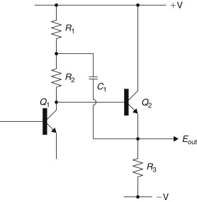
The need for a very low input circuit impedance to minimize thermal noise effects has been met in a number of commercial designs by simply connecting a number of small signal transistors in parallel to reduce their effective base-emitter circuit resistance. Designs of this type came from Ortofon, Linn/Naim, and Braithwaite and are shown in Figures 7.5–7.7.
Figure 7.5. Ortofon MCA-76 head amplifier.

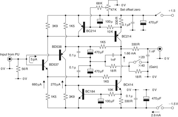
Figure 7.6. The Naim NAC 20 moving coil head amplifier.

Figure 7.7. Braithwaite RAI4 head amplifier. (The output stage is shown in a simplified form.)

If such small signal transistors are used without selection and matching—a time-consuming and expensive process for any commercial manufacturer—some means must be adopted to minimize the effects of the variation in base-emitter turn-on voltage that exist between nominally identical devices because of variations in the doping level in the silicon crystal slice or to other differences in manufacture.
This is achieved in the Ortofon circuit by individual collector-base bias current networks, for which the penalty is the loss of some usable signal in the collector circuit. In the Linn/Naim and Braithwaite designs, this evening out of transistor characteristics in circuits having common base connections is achieved by the use of individual emitter resistors to swamp such differences in device characteristics. In this case, the penalty is that such resistors add to the base-emitter circuit impedance when the task of the design is to reduce this.
7.6.3. Monolithic Super-Matched Input Devices
An alternative method of reducing the input circuit impedance, without the need for separate bias systems or emitter circuit-swamping resistors, is to employ a monolithic (integrated circuit type) device in which a multiplicity of transistors has been simultaneously formed on the same silicon chip. Since these can be assumed to have virtually identical characteristics, they can be paralleled, at the time of manufacture, to give a very low impedance, low noise, matched pair.
An example of this approach is the National Semiconductors LM 194/394 super-match pair, for which a suitable circuit is shown in Figure 7.8. This input device probably offers the best input noise performance currently available, but is relatively expensive.
Figure 7.8. Head amplifier using a LM394 multiple transistor array.

7.6.4. Small Power Transistors as Input Devices
The base-emitter impedance of a transistor depends largely on the size of the junction area on the silicon chip. This will be larger in power transistors than in small signal transistors, which mainly employ relatively small chip sizes. Unfortunately, the current gain of power transistors tends to decrease at low collector current levels, making them unsuitable for this application.
However, use of the plastic encapsulated medium power (3–4 A lc max.) styles, in T0126, T0127, and T0220 packages, at collector currents in the range of 1–3 mA, achieves a satisfactory compromise between input circuit impedance and transistor performance and allows the design of very linear low-noise circuitry. Two examples of MC head amplifier designs of this type, by the author, are shown in Figures 7.9 and 7.10.
Figure 7.9. Cascode input moving coil head amplifier.
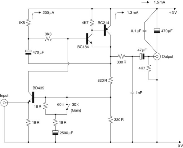
Figure 7.10. Very low-noise, low-distortion, symmetrical MC head amplifier.
The penalty in this case is that, because such transistor types are not specified for low noise operation, some preliminary selection of the devices is desirable, although, in the writer’s experience, the bulk of the devices of the types shown will be found to be satisfactory in this respect.
In the circuit shown in Figure 7.9, the input device is used in the common base (cascode) configuration so that the input current generated by the PU cartridge is transferred directly to the higher impedance point at the collector of this transistor so that the stage gain, prior to the application of negative feedback to the input transistor base, is simply the impedance transformation due to the input device.
In the circuit of Figure 7.10, the input transistors are used in a more conventional common-emitter mode, but the two input devices, although in a push–pull configuration, are effectively connected in parallel so far as the input impedance and noise figure are concerned. The very high degree of symmetry of this circuit assists in minimizing both harmonic and transient distortions.
Both of these circuits are designed to operate from 3-V DC “pen cell” battery supplies to avoid the introduction of mains hum due to the power supply circuitry or to earth loop effects. In mains-powered head amps, great care is always necessary to avoid supply line signal or noise intrusions in view of the very low signal levels at both the inputs and the outputs of the amplifier stage.
It is also particularly advisable to design such amplifiers with single point “0-V” line and supply line connections, which should be coupled by a suitable combination of good quality decoupling capacitors.
7.6.5. Very Low Noise IC Op-Amps
The development, some years ago, of very low noise IC operational amplifiers, such as the Precision Monolithics OP-27 and OP-37 devices, has led to the proliferation of very high-quality, low-noise, low-distortion ICs aimed specifically at the audio market, such as the Signetics NE-5532/ 5534, the NS LM833, the PMI SSM2134/2139, and the TI TL051/052 devices.
With ICs of this type, it is a simple matter to design a conventional RIAA input stage in which the provision of a high-sensitivity, low-noise, moving coil PU input is accomplished by simply reducing the value of the input load resistor and increasing the gain of the RIAA stage in comparison with that needed for higher output PU types. An example of a typical Japanese design of this type is shown in Figure 7.11.
Figure 7.11. Moving coil/moving magnet RIAA input stage in a Technics SU-V10 amplifier.

7.6.6. Other Approaches
A very ingenious, fully symmetrical circuit arrangement that allows the use of normal circuit layouts and components in ultralow noise (e.g., moving coil PU and similar signal level) inputs has been introduced by “Ouad” (Quad Electroacoustics Ltd.) and is employed in all their current series of preamps. This exploits the fact that, at low input signal levels, bipolar junction transistors will operate quite satisfactorily with their base and collector junctions at the same DC potential and permits the type of input circuit shown in Figure 7.12.
Figure 7.12. The “Quad” ultralow noise input circuit layout.
In the particular circuit shown, that used in the “Quad 44” disc input, a two-stage equalization layout is employed, using the type of structure illustrated in Figure 7.4(g), with the gain of the second stage amplifier (a TL071 IC op-amp) switchable to suit the type of input signal level available.
7.7. Input Connections
For all low-level input signals, care must be taken to ensure that the connections are of low contact resistance. This is obviously an important matter in the case of low-impedance circuits such as those associated with MC PU inputs, but is also important in higher impedance circuitry, as the resistance characteristics of poor contacts are likely to be nonlinear, and to introduce both noise and distortion.
In the better class modern units, the input connectors will invariably be of the “phono” type, and both the plugs and the connecting sockets will be gold plated to reduce the problem of poor connections as a consequence of contamination or tarnishing of the metallic contacts.
The use of separate connectors for L and R channels also lessens the problem of interchannel breakthrough due to capacitative coupling or leakage across the socket surface, a problem that can arise in the five- and seven-pin DIN connectors if they are fitted carelessly, particularly when both inputs and outputs are taken to that same DIN connector.
7.8. Input Switching
The comments made about input connections are equally true for the necessary switching of the input signal sources. Separate, but mechanically interlinked, switches of the push-on, push-off type are to be preferred to the ubiquitous rotary wafer switch, in that it is much easier, with separate switching elements, to obtain the required degree of isolation between inputs and channels than would be the case when the wiring is crowded around the switch wafer.
However, even with separate push switches, the problem remains that the input connections will invariably be made to the rear of the amplifier/preamplifier unit, whereas the switching function will be operated from the front panel so that the internal connecting leads must traverse the whole width of the unit.
Other switching systems, based on relays, or bipolar or field effect transistors, have been introduced to lessen the unwanted signal intrusions, which may arise on a lengthy connecting lead. The operation of a relay, which will behave simply as a remote switch when its coil is energized by a suitable DC supply, is straightforward, although for optimum performance it should either be hermetically sealed or have noble metal contacts to resist corrosion.
7.8.1. Transistor Switching
Typical bipolar and FET input switching arrangements are shown in Figures 7.13 and 7.14. In the case of the bipolar transistor switch circuit of Figure 7.13, the nonlinearity of the junction device when conducting precludes its use in the signal line; the circuit is therefore arranged so that the transistor is nonconducting when the signal is passing through the controlled signal channel, but acts as a short-circuit to shunt the signal path to the 0-V line when it is caused to conduct.
Figure 7.13. Bipolar transistor-operated shunt switching. [Also suitable for small-power metal–oxide–semiconductor field-effect transistor (MOSFET) devices.]

Figure 7.14. Junction FET input switching circuit.

In the case of the FET switch, if R1 and R2 are high enough, the nonlinearity of the conducting resistance of the FET channel will be swamped, and the harmonic and other distortions introduced by this device will be negligible (typically less than 0.02% at 1 V rms and 1 kHz).
The CMOS bilateral switches of the CD4066 type are somewhat nonlinear and have a relatively high level of breakthrough. For these reasons they are generally thought to be unsuitable for high-quality audio equipment where such remote switching is employed to minimize cross talk and hum pick up.
However, such switching devices could well offer advantages in lower quality equipment where the cost savings is being able to locate the switching element on the printed circuit board, at the point where it was required, might offset the device cost.
7.8.2. Diode Switching
Diode switching of the form shown in Figure 7.15, while employed very commonly in RF circuitry, is unsuitable for audio use because of the large shifts in the DC level between the “on” and “off” conditions, which would produce intolerable “bangs” on operation.
Figure 7.15. Typical diode switching circuit, as used in RF applications.

For all switching, quietness of operation is an essential requirement, and this demands that care shall be taken to ensure that all of the switched inputs are at the same DC potential, preferably that of the 0-V line. For this reason, it is customary to introduce DC blocking capacitors on all input lines, as shown in Figure 7.16, and the time constants of the input RC networks should be chosen so that there is no unwanted loss of low-frequency signals due to this cause.
Figure 7.16. Use of DC blocking capacitors to minimize input switching noises.

Voltage amplifiers and controls
7.9. Preamplifier Stages
The popular concept of hi-fi attributes the major role in final sound quality to the audio power amplifier and the output devices or output configuration that it uses. Yet in reality the preamplifier system, used with the power amplifier, has at least as large an influence on the final sound quality as the power amplifier, and the design of the voltage gain stages within the pre- and power amplifiers is just as important as that of the power output stages. Moreover, developments in the design of such voltage amplifier stages have allowed continuing improvement in amplifier performance.
The developments in solid-state linear circuit technology that have occurred over the past 30 years seem to have been inspired in about equal measure by the needs of linear integrated circuits and by the demands of high-quality audio systems; engineers working in both of these fields have watched each other’s progress and borrowed from each other’s designs.
In general, the requirements for voltage gain stages in both audio amplifiers and integrated-circuit operational amplifiers are very similar. These are that they should be linear, which implies that they are free from waveform distortion over the required output signal range, have as high a stage gain as is practicable, have a wide AC bandwidth and a low noise level, and are capable of an adequate output voltage swing.
The performance improvements that have been made over this period have been due in part to the availability of new or improved types of semiconductor devices and in part to a growing understanding of the techniques for the circuit optimization of device performance. The interrelation of these aspects of circuit design is considered next.
7.10. Linearity
7.10.1. Bipolar Transistors
In the case of a normal bipolar (NPN or PNP) silicon junction transistor, for which the chip cross section and circuit symbol are shown in Figure 7.17, the major problem in obtaining good linearity lies in the nature of the base voltage/collector current transfer characteristic, shown in the case of a typical “NPN” device (a “PNP” device would have a very similar characteristic, but with negative voltages and currents) in Figure 7.18.
Figure 7.17. Typical chip cross section of NPN and PNP silicon planar epitaxial transistors.

Figure 7.18. Typical transfer characteristic of a silicon transistor.

In this, it can be seen that the input/output transfer characteristic is strongly curved in the region “X–Y” and that an input signal applied to the base of such a device, which is forward biased to operate within this region, would suffer from the very prominent (second harmonic) waveform distortion shown in Figure 7.19.
Figure 7.19. Transistor amplifier waveform distortion due to transfer characteristics.

The way this type of nonlinearity is influenced by the signal output level is shown in Figure 7.20. It is normally found that the distortion increases as the output signal increases, and conversely.
Figure 7.20. Relationship between signal distortion and output signal voltage in a bipolar transistor amplifier.

There are two major improvements in the performance of such a bipolar amplifier stage that can be envisaged from these characteristics. First, because the nonlinearity is due to the curvature of the input characteristics of the device—the output characteristics, shown in Figure 7.21, are linear—the smaller the input signal that is applied to such a stage, the lower the nonlinearity, so that a higher stage gain will lead to reduced signal distortion at the same output level. Second, the distortion due to such a stage is very largely second harmonic in nature.
Figure 7.21. Output current/voltage characteristics of a typical silicon bipolar transistor.

This implies that a “push–pull” arrangement, such as the so-called “long-tailed pair” circuit shown in Figure 7.22, which tends to cancel second harmonic distortion components, will greatly improve the distortion characteristics of such a stage.
Figure 7.22. Transistor voltage amplifier using a long-tailed pair circuit layout.

Also, because the output voltage swing for a given input signal (the stage gain) will increase as the collector load (R2 in Figure 7.22) increases, the higher the effective impedance of this, the lower the distortion that will be introduced by the stage, for any given output voltage signal.
If a high value resistor is used as the collector load for Q1 in Figure 7.22, either a very high supply line voltage must be applied, which may exceed the voltage ratings of the devices, or the collector current will be very small, which will reduce the gain of the device and therefore tend to diminish the benefit arising from the use of a higher value load resistor.
Various circuit techniques have been evolved to circumvent this problem by producing high dynamic impedance loads, which nevertheless permit the amplifying device to operate at an optimum value of collector current. These techniques are discussed later.
An unavoidable problem associated with the use of high values of collector load impedance as a means of attaining high stage gains in such amplifier stages is that the effect of “stray” capacitances, shown as Cs in Figure 7.23, is to cause the stage gain to decrease at high frequencies as the impedance of the stray capacitance decreases and progressively begins to shunt the load. This effect is shown in Figure 7.24, in which the “transition” frequency, fo (the –3-dB gain point) is that frequency at which the shunt impedance of the stray capacitance is equal to that of the load resistor, or its effective equivalent, if the circuit design is such that an “active load” is used in its place.
Figure 7.23. Circuit effect of stray capacitance.

Figure 7.24. Influence of circuit stray capacitances on stage gain.

7.10.2. Field Effect Devices
Other devices that may be used as amplifying components are field effect transistors and MOS devices. Both of these components are very much more linear in their transfer characteristics but have a very much lower mutual conductance (Gm).
This is a measure of the rate of change of output current as a function of an applied change in input voltage. For all bipolar devices, this is strongly dependent on collector current and is, for a small signal silicon transistor, typically of the order of 45 mA/V per mA collector current. Power transistors, operating at relatively high collector currents, for which a similar relationship applies, may therefore offer mutual conductances in the range of amperes/volt.
Because the output impedance of an emitter follower is approximately 1/Gm, power output transistors used in this configuration can offer very low values of output impedance, even without externally applied negative feedback.
All field effect devices have very much lower values for Gm, which will lie, for small-signal components, in the range 2–10 mA/V, not significantly affected by drain currents. This means that amplifier stages employing field-effect transistors, although much more linear, offer much lower stage gains, with other things being equal.
The transfer characteristics of junction (bipolar) FETs, and enhancement and depletion mode MOSFETS are shown in Figure 7.25.
Figure 7.25. Gate voltage versus drain current characteristics of field-effect devices.


7.10.2.1. Metal–Oxide–Semiconductor Field-Effect Transistors
Metal–oxide–semiconductor field-effect transistors, in which the gate electrode is isolated from the source/drain channel, have very similar transfer characteristics to that of junction FETs. They have an advantage that, since the gate is isolated from the drain/source channel by a layer of insulation, usually silicon oxide or nitride, no maximum forward gate voltage can be applied—within the voltage breakdown limits of the insulating layer. In a junction FET the gate, which is simply a reverse biased PN diode junction, will conduct if a forward voltage somewhat in excess of 0.6 V is applied.
The chip constructions and circuit symbols employed for small signal lateral MOSFETs and junction FETs (known simply as FETs) are shown in Figures 7.26 and 7.27.
Figure 7.26. Chip cross section and circuit symbol for lateral MOSFET (small signal type).

Figure 7.27. Chip cross section and circuit symbols for (bipolar) junction FET.


It is often found that the chip construction employed for junction FETs is symmetrical, so that the source and drain are interchangeable in use. For such devices the circuit symbol shown in Figure 7.27(c) should be used properly.
A practical problem with lateral devices, in which the current flow through the device is parallel to the surface of the chip, is that the path length from source to drain, and hence the device impedance and current carrying capacity, is limited by the practical problems of defining and etching separate regions that are in close proximity during the manufacture of the device.
7.10.2.2. V-MOS and T-MOS
This problem is not of very great importance for small signal devices, but is a major concern in high current ones such as those employed in power output stages. It has led to the development of MOSFETs in which the current flow is substantially in a direction that is vertical to the surface and in which the separation between layers is determined by diffusion processes rather than by photolithographic means.
Devices of this kind, known as V-MOS and T-MOS constructions, are shown in Figure 7.28.
Figure 7.28. Power MOSFET constructions using (a) V and (b) T configurations. (Practical devices will employ many such cells in parallel.)


Although these were originally introduced for power output stages, the electrical characteristics of such components are so good that these have been introduced, in smaller power versions, specifically for use in small signal linear amplifier stages. Their major advantages over bipolar devices, having equivalent chip sizes and dissipation ratings, are their high input impedance, their greater linearity, and their freedom from “hole storage” effects if driven into saturation.
These qualities are increasingly attracting the attention of circuit designers working in the audio field, where there is a trend toward the design of amplifiers having a very high intrinsic linearity rather than relying on the use of negative feedback to linearize an otherwise worse design.
7.10.2.3. Breakdown
A specific problem that arises in small signal MOSFET devices is that, because the gate-source capacitance is very small, it is possible to induce breakdown of the insulating layer, which destroys the device, as a result of transferred static electrical charges arising from mishandling.
Although widely publicized and the source of much apprehension, this problem is actually very rarely encountered in use, as small signal MOSFETs usually incorporate protective zener diodes to prevent this eventuality, and power MOSFETs, where such diodes may not be used because they may lead to inadvertent “thyristor” action, have such a high gate-source capacitance that this problem does not normally arise.
In fact, when such power MOSFETs do fail, it is usually found to be because of circuit design defects, which have either allowed excessive operating potentials to be applied to the device, or have permitted inadvertent VHF oscillation, which has led to thermal failure.
7.11. Noise Levels
Improved manufacturing techniques have lessened the differences between the various types of semiconductor devices in respect to intrinsic noise level. For most practical purposes it can now be assumed that the characteristics of the device will be defined by the thermal noise figure of the circuit impedances. This relationship is shown in the graph of Figure 7.29.
Figure 7.29. Thermal noise output as a function of circuit impedance.

For very low noise systems, operating at circuit impedance levels that have been deliberately chosen to be as low as practicable—such as in moving coil PU head amplifiers—bipolar junction transistors are still the preferred device. These will either be chosen to have a large base junction area or will be employed as a parallel-connected array, as, for example, in the LM194/394 “super-match pair” ICs, where a multiplicity of parallel-connected transistors are fabricated on a single chip, giving an effective input (noise) impedance as low as 40 ohms.
However, recent designs of monolithic-dual J-FETs, using a similar type of multiple parallel-connection system, such as the Hitachi 2SK389, can offer equivalent thermal noise resistance values as low as 33 ohms and a superior overall noise figure at input resistance values in excess of 100 ohms.
At impedance levels beyond about 1 kilohm there is little practical difference between any devices of recent design. Earlier MOSFET types were not so satisfactory because of excess noise effects arising from carrier-trapping mechanisms in impurities at the channel/gate interface.
7.12. Output Voltage Characteristics
Since it is desirable that output overload and signal clipping do not occur in audio systems, particularly in stages preceding the gain controls, much emphasis has been placed on the so-called “headroom” of signal handling stages, especially in hi-fi publications where the reviewers are able to distance themselves from the practical problems of circuit design.
While it is obviously desirable that inadvertent overload shall not occur in stages preceding signal level controls, high levels of feasible output voltage swing demand the use of high voltage supply rails, which, in turn, demand the use of active components that can support such working voltage levels.
Not only are such devices more costly, but they will usually have poorer performance characteristics than similar devices of lower voltage ratings. Also, the requirement for the use of high voltage operation may preclude the use of components having valuable characteristics, but which are restricted to lower voltage operation.
Practical audio circuit designs will therefore regard headroom simply as one of a group of desirable parameters in a working system whose design will be based on careful consideration of the maximum input signal levels likely to be found in practice.
Nevertheless, improved transistor or IC types, and new developments in circuit architecture, are welcomed as they occur and have eased the task of the audio design engineer, for whom the advent of new program sources, in particular the compact disc, and now digital audio tape systems, has greatly extended the likely dynamic range of the output signal.
7.12.1. Signal Characteristics
The practical implications of this can be seen from a consideration of the signal characteristics of existing program sources. Of these, in the past, the standard vinyl (“black”) disc has been the major determining factor. In this, practical considerations of groove tracking have limited the recorded needle tip velocity to about 40 cm/s, and typical high-quality PU cartridges capable of tracking this recorded velocity will have a voltage output of some 3 mV at a standard 5-cm/s recording level.
If the preamplifier specification calls for maximum output to be obtainable at a 5-cm/s input, then the design should be chosen so that there is a “headroom factor” of at least 8× in such stages preceding the gain controls.
In general, neither FM broadcasts, where the dynamic range of the transmitted signal is limited by the economics of transmitter power, nor cassette recorders, where the dynamic range is constrained by the limited tape overload characteristics, have offered such a high practicable dynamic range.
It is undeniable that the analogue tape recorder, when used at 15 in/s, twin-track, will exceed the LP record in dynamic range. After all, such recorders were originally used for mastering the discs. But such program sources are rarely found except among “live recording” enthusiasts. However, the compact disc, which is becoming increasingly common among purely domestic hi-fi systems, presents a new challenge, as the practicable dynamic range of this system exceeds 80 dB (10,000:1), and the likely range from mean (average listening level) to peak may well be as high as 35 dB (56:1) in comparison with the 18-dB (8:1) range likely with the vinyl disc.
Fortunately, because the output of the compact disc player is at a high level, typically 2 V rms, and requires no signal or frequency response conditioning prior to use, the gain control can be sited directly at the input of the preamp. Nevertheless, this still leaves the possibility that signal peaks may occur during use that are some 56× greater than the mean program level, with the consequence of the following amplifier stages being driven hard into overload.
This has refocused attention on the design of solid-state voltage amplifier stages having a high possible output voltage swing and upon power amplifiers that either have very high peak output power ratings or more graceful overload responses.
7.13. Voltage Amplifier Design
The sources of nonlinearity in bipolar junction transistors have already been referred to, in respect to the influence of collector load impedance, and push–pull symmetry in reducing harmonic distortion. An additional factor with bipolar junction devices is the external impedance in the base circuit, as the principal nonlinearity in a bipolar device is that due to its input voltage/output current characteristics. If the device is driven from a high impedance source, its linearity will be substantially greater, since it is operating under conditions of current drive.
This leads to the good relative performance of the simple, two-stage, bipolar transistor circuit of Figure 7.30 in that the input transistor, Q1, is only required to deliver a very small voltage drive signal to the base of Q2 so that the signal distortion due to Q1 will be low. Q2, however, which is required to develop a much larger output voltage swing, with a much greater potential signal nonlinearity, is driven from a relatively high source impedance, composed of the output impedance of Q1, which is very high indeed, in parallel with the base-emitter resistor, R4. R1, R2, and R3/C2 are employed to stabilize the DC working conditions of the circuit.
Figure 7.30. A two-stage transistor voltage amplifier.

Normally, this circuit is elaborated somewhat to include both DC and AC negative feedback from the collector of Q2 to the emitter of Q1, as shown in the practical amplifier circuit of Figure 7.31.
Figure 7.31. A practical two-transistor feedback amplifier.

This is capable of delivering a 14-V p-p output swing, at a gain of 100, and a bandwidth of 15 Hz to 250 kHz, at −3-dB points; largely determined by the value of C2 and the output capacitances, with a THD figure of better that 0.01% at 1 kHz.
The practical drawbacks of this circuit relate to the relatively low value necessary for R3—with the consequent large value necessary for C2 if a good LF response is desired, and the DC offset between point ‘X’ and the output, due to the base-emitter junction potential of Q1, and the DC voltage drop along R5, which makes this circuit relatively unsuitable in DC amplifier applications.
An improved version of this simple two-stage amplifier circuit is shown in Figure 7.32, in which the single input transistor has been replaced by a “long-tailed pair” configuration of the type shown in Figure 7.32. In this, if the two-input transistors are reasonably well matched in current gain and if the value of R3 is chosen to give an equal collector current flow through both Q1 and Q2, the DC offset between input and output will be negligible, which will allow the circuit to be operated between symmetrical (+ and −) supply rails over a frequency range extending from DC to 250 kHz or more.
Figure 7.32. Improved two-stage feedback amplifier.

Because of the improved rejection of odd harmonic distortion inherent in the input “push–pull” layout, the THD due to this circuit, particularly at less than maximum output voltage swing, can be extremely low, which probably forms the basis of the bulk of linear amplifier designs. However, further technical improvements are possible, which are discussed next.
7.14. Constant-Current Sources and “Current Mirrors”
As mentioned earlier, the use of high-value collector load resistors in the interests of high stage gain and low inherent distortion carries with it the penalty that the performance of the amplifying device may be impaired by the low collector current levels that result from this approach.
Advantage can, however, be taken of the very high output impedance of a junction transistor, which is inherent in the type of collector current/supply voltage characteristics illustrated in Figure 7.21, where even at currents in the 1- to 10-mA region, dynamic impedances of the order of 100 kilohms may be expected.
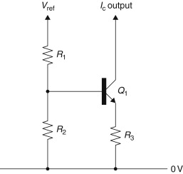
A typical circuit layout that utilizes this characteristic is shown in Figure 7.33, in which R1 and R2 form a potential divider to define the base potential of Q1, and R3 defines the total emitter or collector currents for this effective base potential.
Figure 7.33. Transistor constant current source.
This configuration can be employed with transistors of either PNP or NPN types, which allow the circuit designer considerable freedom in their application.
An improved, two-transistor, constant current source is shown in Figure 7.34. In this, R1 is used to bias Q2 into conduction, and Q1 is employed to sense the voltage developed across R2, which is proportional to emitter current, and to withdraw the forward bias from Q2 when that current level is reached at which the potential developed across R2 is just sufficient to cause Q1 to conduct.
Figure 7.34. Two-transistor constant current source.

The performance of this circuit is greatly superior to that of Figure 7.33 in that the output impedance is about 10× greater and the circuit is insensitive to the potential, +Vref., applied to R1, so long as it is adequate to force both Q2 and Q1 into conduction.
An even simpler circuit configuration makes use of the inherent very high output impedance of a junction FET under constant gate bias conditions. This employs the circuit layout shown in Figure 7.35, which allows a true “two-terminal” constant current source, independent of supply lines or reference potentials, and which can be used at either end of the load chain.
Figure 7.35. Two-terminal constant current source.

The current output from this type of circuit is controlled by the value chosen for R1, and this type of constant current source may be constructed using almost any available junction FET, provided that the voltage drop across the FET drain-gate junction does not exceed the breakdown voltage of the device. This type of constant current source is also available as small, plastic-encapsulated, two-lead devices, at a relatively low cost, and with a range of specified output currents.
All of these constant current circuit layouts share the common small disadvantage that they will not perform very well at low voltages across the current source element. In the case of Figures 7.33 and 7.34, the lowest practicable operating potential will be about 1 V. The circuit of Figure 7.35 may require, perhaps, 2–3 V, and this factor must be considered in circuit performance calculations.
The “boot-strapped” load resistor arrangement shown in Figure 7.36, and commonly used in earlier designs of audio amplifier to improve the linearity of the last class ‘A’ amplifier stage (Q1), effectively multiplies the resistance value of R2 by the gain which Q2 would be deemed to have if operated as a common-emitter amplifier with a collector load of R3 in parallel with R1.
Figure 7.36. Load impedance increase by boot-strap circuit.
This arrangement is the best configuration practicable in terms of available rms output voltage swing as compared with conventional constant current sources, but has fallen into disuse because it leads to slightly lower quality THD figures than are possible with other circuit arrangements.
All these circuit arrangements suffer from a further disadvantage, from the point of view of the integrated circuit designer: they employ resistors as part of the circuit design, and resistors, although possible to fabricate in IC structures, occupy a disproportionately large area of the chip surface. Also, they are difficult to fabricate to precise resistance values without resorting to subsequent laser trimming, which is expensive and time-consuming.
Because of this, there is a marked preference on the part of IC design engineers for the use of circuit layouts known as “current mirrors,” of which a simple form is shown in Figure 7.37.
Figure 7.37. Simple form of a current mirror.

7.14.1. IC Solutions
These are not true constant current sources in that they are only capable of generating an output current (Lout) that is a close equivalent of the input or drive current (Lin). However, the output impedance is very high, and if the drive current is held to a constant value, the output current will also remain constant.
A frequently found elaboration of this circuit, which offers improvements in respect to output impedance and the closeness of equivalence of the drive and output currents, is shown in Figure 7.38. Like the junction FET-based constant current source, these current mirror devices are available as discrete, plastic-encapsulated, three-lead components, having various drive current/output current ratios, for incorporation into discrete component circuit designs.
Figure 7.38. Improved form of a current mirror.

The simple amplifier circuit of Figure 7.32 can be elaborated, as shown in Figure 7.39, to employ these additional circuit refinements, which would have the effect of increasing the open-loop gain, that is, that before negative feedback is applied, by 10−100× and improving the harmonic and other distortions, and the effective bandwidth by perhaps 3−10×. From the point of view of the IC designer, there is also the advantage of a potential reduction in the total resistor count.
Figure 7.39. Use of circuit elaboration to improve the two-stage amplifier of Figure 7.32.

These techniques for improving the performance of semiconductor amplifier stages find particular application in the case of circuit layouts employing junction FETs and MOSFETs, where the lower effective mutual conductance values for the devices would normally result in relatively poor stage gain figures.
This has allowed the design of IC operational amplifiers, such as the RCA CA3140 series or the Texas Instruments TL071 series, which employ, respectively, MOSFET and junction FET input devices. The circuit layout employed in the TL071 is shown, by way of example, in Figure 7.40.
Figure 7.40. Circuit layout of Texas Instruments TL071 op-amp.

Both of these op-amp designs offer input impedances in the million megohm range— in comparison with the input impedance figures of 5–10 kilohm, which were typical of early bipolar ICs—and the fact that the input impedance is so high allows the use of such ICs in circuit configurations for which earlier op-amp ICs were entirely inappropriate.
Although the RCA design employs MOSFET input devices, which offer, in principle, an input impedance that is perhaps 1000 times better than this figure, the presence of on-chip Zener diodes, to protect the device against damage through misuse or static electric charges, reduces the input impedance to roughly the same level as that of the junction FET device.
It is a matter for some regret that the design of the CA3140 series devices is now so elderly that the internal MOSFET devices do not offer the low level of internal noise of which more modern MOSFET types are capable. This tends to rule out the use of this MOSFET op-amp for high-quality audio use, although the TL071 and its equivalents, such as the LF351, have demonstrated impeccable audio behavior.
7.15. Performance Standards
It has always been accepted in the past, and is still held as axiomatic among a very large section of the engineering community, that performance characteristics can be measured and that improved levels of measured performance will correlate precisely, within the ability of the ear to detect such small differences, with improvements that the listener will hear in reproduced sound quality.
Within a strictly engineering context, it is difficult to do anything other than accept the concept that measured improvements in performance are the only things that should concern the designer.
However, the frequently repeated claim by journalists and reviewers working for periodicals in the hi-fi field—who, admittedly, are unlikely to be unbiased witnesses—that measured improvements in performance do not always go hand in hand with the impressions that the listener may form, tends to undermine the confidence of the circuit designer that the instrumentally determined performance parameters are all that matter.
It is clear that it is essential for engineering progress that circuit design improvements must be sought that lead to measurable performance improvements. However, there is now also the more difficult criterion that those things that appear to be better, in respect to measured parameters, must also be seen, or heard, to be better.
7.15.1. Use of ICs
This point is particularly relevant to the question of whether, in very high-quality audio equipment, it is acceptable to use IC operational amplifiers, such as the TL071, or some of the even more exotic later developments such as the NE5534 or the OP27, as the basic gain blocks, around which the passive circuitry can be arranged, or whether, as some designers believe, it is preferable to construct such gain blocks entirely from discrete components.
Some years ago, there was a valid technical justification for this reluctance to use op-amp ICs in high-quality audio circuitry, as the method of construction of such ICs was as shown, schematically, in Figure 7.41, in which all the structural components were formed on the surface of a heavily ‘P’ doped silicon substrate, and relied for their isolation from one another or from the common substrate on the reverse-biased diodes formed between these elements.
Figure 7.41. Method of fabrication of components in a silicon-integrated circuit.

This led to a relatively high residual background noise level, in comparison with discrete component circuitry, due to the effects of the multiplicity of reverse diode leakage currents associated with every component on the chip. Additionally, there were quality constraints in respect to the components formed on the chip surface—more severe for some component types than for others—that also impaired the circuit performance.
A particular instance of this problem arose in the case of PNP transistors used in normal ICs, where the circuit layout did not allow these to be formed with the substrate acting as the collector junction. In this case, it was necessary to employ the type of construction known as a “lateral PNP,” in which all the junctions are diffused in, from the exposed chip surface, side by side.
In this type of device the width of the ‘N’ type base region, which must be very small for optimum results, depends mainly on the precision with which the various diffusion masking layers can be applied. The results are seldom very satisfactory. Such a lateral PNP device has a very poor current gain and HF performance.
In recent IC designs, considerable ingenuity has been shown in the choice of circuit layout to avoid the need to employ such unsatisfactory components in areas where their shortcomings would affect the end result. Substantial improvements, both in the purity of the base materials and in diffusion technology, have allowed the inherent noise background to be reduced to a level where it is no longer of practical concern.
7.15.2. Modern Standards
The standard of performance that is now obtainable in audio applications, from some of the recent IC op–amps, especially at relatively low closed-loop gain levels, is frequently of the same order as that of the best discrete component designs, but with considerable advantages in other respects, such as cost, reliability, and small size.
This has led to their increasing acceptance as practical gain blocks, even in very high-quality audio equipment.
When blanket criticism is made of the use of ICs in audio circuitry, it should be remembered that the 741, which was one of the earliest of these ICs to offer a satisfactory performance—although it is outclassed by more recent types—has been adopted with enthusiasm, as a universal gain block, for the signal handling chains in many recording and broadcasting studios.
This implies that the bulk of the program signals employed by the critics to judge whether or not a discrete component circuit is better than that using an IC will already have passed through a sizeable handful of 741-based circuit blocks, and if such ICs introduce audible defects, then their reference source is already suspect.
It is difficult to stipulate the level of performance that will be adequate in a high-quality audio installation. This arises partly because there is little agreement between engineers and circuit designers, on the one hand, and the hi-fi fraternity, on the other hand, about the characteristics that should be sought and partly because of the wide differences that exist between listeners in their expectations for sound quality or their sensitivity to distortions. These differences combine to make it a difficult and speculative task to attempt either to quantify or to specify the technical components of audio quality or to establish an acceptable minimum-quality level.
Because of this uncertainty, the designer of equipment in which price is not a major consideration will normally seek to attain standards substantially in excess of those that he supposes to be necessary, simply in order not to fall short. This means that the reason for the small residual differences in the sound quality, as between high-quality units, is the existence of malfunctions of types that are not currently known or measured.
7.16. Audibility of Distortion
7.16.1. Harmonic and Intermodulation Distortion
Because of the small dissipations that are normally involved, almost all discrete component voltage amplifier circuitry will operate in class ‘A’ (that condition in which the bias applied to the amplifying device is such as to make it operate in the middle of the linear region of its input/output transfer characteristic), and the residual harmonic components are likely to be mainly either second or third order, which are audibly much more tolerable than higher order distortion components.
Experiments in the late 1940s suggested that the level of audibility for second and third harmonics was of the order of 0.6 and 0.25%, respectively, which led to the setting of a target value, within the audio spectrum, of 0.1% THD, as desirable for high-quality audio equipment.
However, recent work aimed at discovering the ability of an average listener to detect the presence of low-order (i.e., second or third) harmonic distortions has drawn the uncomfortable conclusion that listeners, taken from a cross section of the public, may rate a signal to which 0.5% second harmonic distortion has been added as “more musical” than, and therefore preferable to, the original undistorted input. This discovery tends to cast doubt on the value of some subjective testing of equipment.
What is not in dispute is that the intermodulation distortion (IMD), which is associated with any nonlinearity in the transfer characteristics, leads to a muddling of the sound picture so that if the listener is asked not which sound he prefers, but which sound seems to him to be the clearer, he will generally choose that with the lower harmonic content.
The way in which IMD arises is shown in Figure 7.42, where a composite signal containing both high-frequency and low-frequency components, fed through a nonlinear system, causes each signal to be modulated by the other. This is conspicuous in the drawing in respect to the HF component, but is also true for the LF one.
Figure 7.42. Intermodulation distortions produced by the effect of a nonlinear input/output transfer characteristic on a complex tone.

This can be shown mathematically to be due to the generation of sum and difference products, in addition to the original signal components, and provides a simple method, shown schematically in Figure 7.43, for the detection of this type of defect. A more formal IMD measurement system is shown in Figure 7.44.
Figure 7.43. Simple HF two-tone intermodulation distortion test.

Figure 7.44. Two-tone intermodulation distortion test rig.

With present circuit technology and device types, it is customary to design for total harmonic and IM distortions to be below 0.01% over the range 30 Hz–20 kHz, and at all signal levels below the onset of clipping. Linear IC op-amps, such as the TL071 and the LF351, will also meet this specification over the frequency range 30 Hz–10 kHz.
7.16.2. Transient Defects
A more insidious group of signal distortions may occur when brief signals of a transient nature, or sudden step type changes in base level, are superimposed on the more continuous components of the program signal. These defects can take the form of slew-rate distortions, usually associated with a loss of signal during the period of the slew-rate saturation of the amplifier—often referred to as transient intermodulation distortion or TID.
This defect is illustrated in Figure 7.45 and arises particularly in amplifier systems employing substantial amounts of negative feedback when there is some slew-rate limiting component within the amplifier, as shown in Figure 7.46.
Figure 7.45. Effect of amplifier slew-rate saturation or transient intermodulation distortion.

Figure 7.46. Typical amplifier layout causing slew-rate saturation.

A further problem is that due to “overshoot,” or “ringing,” on a transient input, as illustrated in Figure 7.47. This arises particularly in feedback amplifiers if there is an inadequate stability margin in the feedback loop, particularly under reactive load conditions, but will also occur in low-pass filter systems if too high an attenuation rate is employed.
Figure 7.47. Transient “ringing.”

The ear is very sensitive to slew-rate induced distortion, which is perceived as a “tizziness” in the reproduced sound. Transient overshoot is normally noted as a somewhat overbright quality. The avoidance of both these problems demands care in the circuit design, particularly when a constant current source is used, as shown in Figure 7.48.
Figure 7.48. Circuit design aspects that may cause slew-rate limiting.
In this circuit, the constant current source, CC1, will impose an absolute limit on the possible rate of change of potential across the capacitance, C1 (which could well be simply the circuit stray capacitance), when the output voltage is caused to move in a positive-going direction. This problem is compounded if an additional current limit mechanism, CC2, is included in the circuitry to protect the amplifier transistor (Q1) from output current overload.
Since output load and other inadvertent capacitances are unavoidable, it is essential to ensure that all such current limited stages operate at a current level that allows potential slewing to occur at rates that are at least 10× greater than the fastest signal components. Alternatively, means may be taken, by way of a simple input integrating circuit, (R1C1), as shown in Figure 7.49, to ensure that the maximum rate of change of the input signal voltage is within the ability of the amplifier to handle it.
Figure 7.49. Input HF limiting circuit to lessen slew-rate limiting.

7.16.3. Spurious Signals
In addition to harmonic, IM, and transient defects in the signal channel, which will show up on normal instrumental testing, there is a whole range of spurious signals that may not arise in such tests. The most common of these is that of the intrusion of noise and alien signals, either from the supply line or by direct radio pick up.
This latter case is a random and capricious problem that can only be solved by steps appropriate to the circuit design in question. However, supply line intrusions, whether because of unwanted signals from the power supply or from the other channel in a stereo system, may be reduced greatly by the use of circuit designs offering a high immunity to voltage fluctuations on the DC supply.
Other steps, such as the use of electronically stabilized DC supplies or the use of separate power supplies in a stereo amplifier, are helpful, but the required high level of supply line signal rejection should be sought as a design feature before other palliatives are applied. Modern IC op-amps offer a typical supply voltage rejection ratio of 90 dB (30,000:1). Good discrete component designs should offer at least 80 dB (10,000:1).
This figure tends to degrade at higher frequencies, which has led to the growing use of supply line bypass capacitors having a low effective series resistance. This feature is either a result of the capacitor design or is achieved in the circuit by the designer’s adoption of groups of parallel connected capacitors chosen so that the AC impedance remains low over a wide range of frequencies.
A particular problem in respect to spurious signals, which occurs in audio power amplifiers, is a consequence of the loudspeaker acting as a voltage generator, when stimulated by pressure waves within the cabinet, and injecting unwanted audio components directly into the negative feedback loop of the amplifier. This specific problem is unlikely to arise in small signal circuitry, but the designer must consider what effect output/line load characteristics may have, particularly in respect to reduced stability margin in a feedback amplifier.
In all amplifier systems there is a likelihood of microphonic effects due to vibration of the components. This is likely to be of increasing importance at the input of “low-level,” high-sensitivity preamplifier stages and can lead to coloration of the signal when the equipment is in use, which is overlooked in the laboratory in a quiet environment.
7.16.4. Mains-Borne Interference
Mains-borne interference, as evidenced by noise pulses on switching electrical loads, is most commonly due to radio pick up problems and is soluble by the techniques (attention to signal and earth line paths, avoidance of excessive HF bandwidth at the input stages) that are applicable to these.
7.17. General Design Considerations
During the past three decades, a range of circuit design techniques has evolved to allow the construction of highly linear gain stages based on bipolar transistors whose input characteristics are, in themselves, very nonlinear. These techniques have also allowed substantial improvements in possible stage gain and have led to greatly improved performance from linear, but low gain, field-effect devices.
These techniques are used in both discrete component designs and in their monolithic integrated circuit equivalents, although, in general, the circuit designs employed in linear ICs are considerably more complex than those used in discrete component layouts.
This is partly dictated by economic considerations, partly by the requirements of reliability, and partly because of the nature of IC design.
The first two of these factors arise because both the manufacturing costs and the probability of failure in a discrete component design are directly proportional to the number of components used, so the fewer the better, whereas in an IC, both the reliability and the expense of manufacture are affected only minimally by the number of circuit elements employed.
In the manufacture of ICs, as indicated earlier, some of the components that must be employed are much worse than their discrete design equivalents. This has led the IC designer to employ fairly elaborate circuit structures, either to avoid the need to use a poor-quality component in a critical position or to compensate for its shortcomings.
Nevertheless, the ingenuity of the designers and the competitive pressures of the market- place have resulted in systems having a very high performance, usually limited only by their inability to accept differential supply line potentials in excess of 36 V unless nonstandard diffusion processes are employed.
For circuitry requiring higher output or input voltage swings than allowed by small signal ICs, the discrete component circuit layout is, at the moment, unchallenged. However, as every designer knows, it is a difficult matter to translate a design that is satisfactory at a low working voltage design into an equally good higher voltage system.
- increased applied potentials produce higher thermal dissipations in the components for the same operating currents;
- device performance tends to deteriorate at higher interelectrode potentials and higher output voltage excursions; and,
- available high/voltage transistors tend to be more restricted in variety and less good in performance than lower voltage types.
7.18. Controls
These fall into a variety of categories:
- gain controls needed to adjust the signal level between source and power amplifier stages;
- tone controls used to modify the tonal characteristics of the signal chain; and,
- filters employed to remove unwanted parts of the incoming signal, and those adjustments used to alter the quality of the audio presentation, such as stereo channel balance or channel separation controls.
7.18.1. Gain Controls
These are the simplest in basic form and are often just a resistive potentiometer voltage divider of the type shown in Figure 7.50. Although simple, this component can generate a variety of problems. Of these, the first is due to the value chosen for R1. Unless this is infinitely high, it will attenuate the maximum signal voltage (Emax) obtainable from the source, in the ratio
![]() where Zsource is the output impedance of the driving circuit. This factor favors the use of a high value for R1 to avoid loss of input signal.
where Zsource is the output impedance of the driving circuit. This factor favors the use of a high value for R1 to avoid loss of input signal.
Figure 7.50. Standard gain control circuit.

However, the following amplifier stage may have specific input impedance requirements and is unlikely to operate satisfactorily unless the output impedance of the gain control circuit is fairly low. This will vary according to the setting of the control, between zero and a value, at the maximum gain setting of the control, due to the parallel impedances of the source and gain control.
![]()
The output impedance at intermediate positions of the control varies as the effective source impedance and the impedance to the 0-V line are altered. However, in general, these factors would encourage the use of a low value for R1.
An additional and common problem arises because the perceived volume level associated with a given sound pressure (power) level has a logarithmic characteristic. This means that the gain control potentiometer, R1, must have a resistance value that has a logarithmic, rather than linear, relationship with the angular rotation of the potentiometer shaft.
7.18.1.1. Potentiometer Law
Since the most common types of control potentiometer employ a resistive composition material to form the potentiometer track, it is a difficult matter to ensure that the grading of conductivity within this material will follow an accurate logarithmic law.
On a single channel this error in the relationship between signal loudness and spindle rotation may be relatively unimportant. In a stereo system, having two ganged gain control spindles, intended to control the loudness of the two channels simultaneously, errors in following the required resistance law, existing between the two potentiometer sections, will cause a shift in the apparent location of the stereo image as the gain control is adjusted, which can be very annoying.
In high-quality equipment, this problem is sometimes avoided by replacing R1 by a precision resistor chain (Ra – Rz), as shown in Figure 7.51, in which the junctions between these resistors are connected to tapping points on a high-quality multiposition switch.
Figure 7.51. Improved gain control using a multi-pole switch.

By this means, if a large enough number of switch tap positions is available, and this implies at least a 20-way switch to give a gentle gradation of sound level, a very close approximation to the required logarithmic law can be obtained, and two such channel controls could be ganged without unwanted errors in the differential output level.
7.18.1.2. Circuit Capacitances
A further practical problem, illustrated in Figure 7.50, is associated with circuit capacitances. First, it is essential to ensure that there is no standing DC potential across R1 in normal operation, as this will cause an unwanted noise in the operation of the control. This imposes the need for a protective input capacitor, C1, which will cause a loss of low-frequency signal components, with a −3-dB LF turnover point at the frequency at which the impedance of Cm is equal to the sum of the source and gain control impedances. C1 should therefore be of an adequate value.
Additionally, there are the effects of the stray capacitances, C2 and C3, associated with the potentiometer construction, and the amplifier input and wiring capacitances, C4. The effect of these is to modify the frequency response of the system, at the HF end, as a result of signal currents passing through these capacitances. The choice of a low value for R1 is desirable to minimize this problem.
The use of the gain control to operate an on/off switch, which is fairly common in low-cost equipment, can lead to additional problems, especially with high resistance value gain control potentiometers, in respect to AC mains “hum” pick up. It also leads to a more rapid rate of wear of the gain control in that it is rotated at least twice whenever the equipment is used.
7.18.2. Tone Controls
These exist in the various forms shown in Figures 7.52–7.56, respectively, described as standard (bass and treble lift or cut), slope control, Clapham junction, parametric, and graphic equalizer types. The effect these will have on the frequency response of the equipment is shown in the drawings, and their purpose is to help remedy shortcomings in the source program material, the receiver or transducer, or in the loudspeaker and listening room combination.
Figure 7.52. Bass and treble lift/cut tone control.
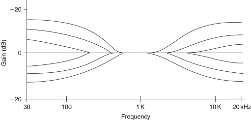
Figure 7.53. Slope control.

Figure 7.54. Clapham junction type of tone control.

Figure 7.55. Parametric equalizer control.

Figure 7.56. Graphic equalizer response characteristics.
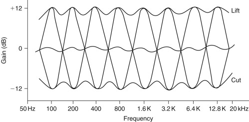
To the hi-fi purist, all such modifications to the input signal tend to be regarded with distaste and are therefore omitted from some hi-fi equipment. However, they can be useful and make valuable additions to the audio equipment, if used with care.
7.18.2.1. Standard Tone Control Systems
These are either of the passive type, of which a typical circuit layout is shown in Figure 7.57, or are constructed as part of the negative feedback loop around a gain block using the general design due to Baxandall. A typical circuit layout for this kind of design is shown in Figure 7.58.
Figure 7.57. Circuit layout of passive tone control.
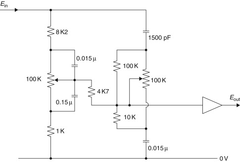
Figure 7.58. Negative feedback type tone control circuit.

It is claimed that the passive layout has an advantage in quality over the active (feedback network) type of control in that the passive network merely contains resistors and capacitors and is therefore free from any possibility of introduced distortion, whereas the “active” network requires an internal gain block, which is not automatically above suspicion.
In reality, however, any passive network must introduce an attenuation, in its fiat response form, which is equal to the degree of boost sought at the maximum “lift” position, and some external gain block must therefore be added to compensate for this gain loss.
This added gain block is just as prone to introduce distortion as that in an active network, with the added disadvantage that it must provide a gain equal to that of the fiat-response network attenuation, whereas the active system gain block will typically have a gain of unity in the fiat response mode, with a consequently lower distortion level.
As a final point, it should be remembered that any treble lift circuit will cause an increase in harmonic distortion, simply because it increases the gain at the frequencies associated with harmonics, in comparison with that at the frequency of the fundamental.
The verdict of the amplifier designers appears to be substantially in favor of the Baxandall system in that this is the layout employed most commonly.
Both of these tone control systems—indeed this is true of all such circuitry—rely for their operation on the fact that the AC impedance of a capacitor will depend on the applied frequency, as defined by the equation:
![]() or, more accurately,
or, more accurately,
![]() where j is the square root of −1.
where j is the square root of −1.
Commonly, in circuit calculations, the 2πf group of terms is lumped together and represented by the Greek symbol ω.
The purpose of the j term, which appears as a “quadrature” element in the algebraic manipulations, is to permit the circuit calculations to take account of the 90° phase shift introduced by the capacitative element. (The same is also true of inductors within such a circuit, except that the phase shift will be in the opposite sense.) This is important in most circuits of this type.
The effect of the change in impedance of the capacitor on the output signal voltage from a simple RC network, of the kind shown in Figures 7.59(a) and 7.60(a), is shown in Figures 7.59(b) and 7.60(b). If a further resistor, R2, is added to the networks, the result is modified in the manner shown in Figures 7.61 and 7.62. This type of structure, elaborated by the use of variable resistors to control the amount of lift or fall of output as a function of frequency, is the basis of the passive tone control circuitry of Figure 7.57.
Figure 7.59. Layout and frequency response of a simple bass-cut circuit (high pass).
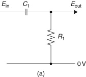

Figure 7.60. Layout and frequency response of a simple treble-cut circuit (low pass).


Figure 7.61. Modified bass-cut (high-pass) RC circuit.

Figure 7.62. A modified treble-cut (low-pass) RC circuit.

If such networks are connected across an inverting gain block, as shown in Figures 7.63(a) and 7.64(a), the resultant frequency response will be shown in Figures 7.63(b) and 7.64(b), since the gain of such a negative feedback configuration will be
![]()
Figure 7.63. Active RC treble-lift or bass-cut circuit.
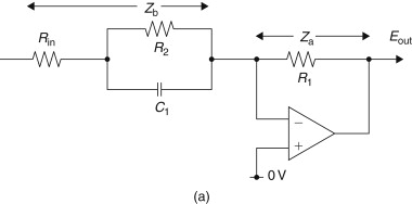
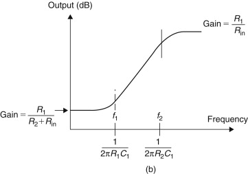
Figure 7.64. Active RC treble-cut or bass-lift circuit.
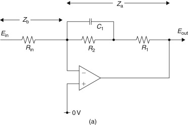

assuming that the open-loop gain of the gain block is sufficiently high. This is the design basis of the Baxandall type of tone control, and a flat frequency response results when the impedance of the input and output limbs of such a feedback arrangement remains in equality as the frequency is varied.
7.18.2.2. Slope Controls
This is the type of tone control employed by Quad in its type 44 preamplifier and operates by altering the relative balance of the LF and HF components of the audio signal, with reference to some specified midpoint frequency, as is shown in Figure 7.53. A typical circuit for this type of design is shown in Figure 7.65.
Figure 7.65. The Quad tilt control.

The philosophical justification for this approach is that it is unusual for any commercially produced program material to be significantly in error in its overall frequency characteristics, but the tonal preferences of the recording or broadcasting balance engineer may differ from those of the listener.
In such a case, he might consider that the signal, as presented, was somewhat overheavy, in respect to its bass, or alternatively, perhaps, that it was somewhat light or thin in tone, and an adjustment of the skew of the frequency response could correct this difference in tonal preference without significantly altering the signal in other respects.
7.18.2.3. The Clapham Junction Type
This type of tone control, whose possible response curves are shown in Figure 7.54, was introduced by the author to provide a more versatile type of tonal adjustment than that offered by the conventional standard systems for remedying specific peaks or troughs in the frequency response, without the penalties associated with the graphic equalizer type of control, described later.
In the Clapham junction type system, so named because of the similarity of the possible frequency response curves to that of railway lines, a group of push switches is arranged to allow one or more of a multiplicity of RC networks to be introduced into the feedback loop of a negative feedback type tone control system, as shown in Figure 7.66, to allow individual ±3-dB frequency adjustments to be made, over a range of possible frequencies.
Figure 7.66. Clapham junction tone control.

By this means it is possible, by combining elements of frequency lift or cut, to choose from a variety of possible frequency response curves without losing the ability to attain a linear frequency response.
7.18.2.4. Parametric Controls
This type of tone control, whose frequency response is shown in Figure 7.55, has elements of similarity to both the standard bass/treble lift/cut systems and the graphic equalizer arrangement in that while there is a choice of lift or cut in the frequency response, the actual frequency at which this occurs may be adjusted, up or down, in order to attain an optimal system frequency response.
A typical circuit layout is shown in Figure 7.67.
Figure 7.67. Parametric equalizer circuit.
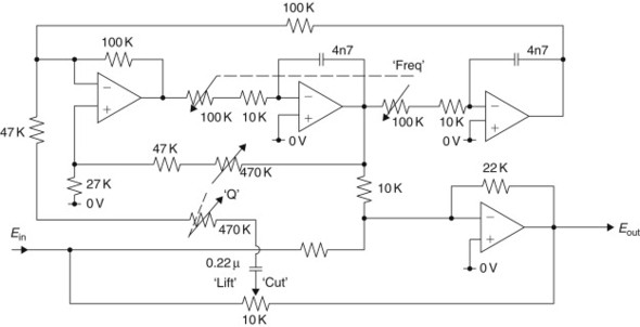
7.18.2.5. The Graphic Equalizer System
The aim of this type of arrangement is to compensate fully for the inevitable peaks and troughs in the frequency response of the audio system, including those due to deficiencies in the loudspeakers or the listening room acoustics, by permitting the individual adjustment of the channel gain, within any one of a group of eight single-octave segments of the frequency band, typically covering the range from 80 Hz to 20 kHz, although 10 octave equalizers covering the whole audio range from 20 Hz to 20 kHz have been offered.
Because the ideal solution to this requirement—that of employing a group of parallel connected amplifiers, each of which is filtered so that it covers a single octave band of the frequency spectrum, whose individual gains could be adjusted separately—would be excessively expensive to implement, conventional practice is to make use of a series of LC-tuned circuits, connected within a feedback control system, as shown in Figure 7.68.
Figure 7.68. Circuit layout for a graphic equalizer (only four sections shown).

This gives the type of frequency response curve shown in Figure 7.56. As can be seen, there is no position of lift or cut, or combination of control settings, that will permit a flat frequency response because of the interaction, within the circuitry, between the adjacent octave segments of the pass band.
While such types of tone control are undoubtedly useful and can make significant improvements in the performance of otherwise unsatisfactory hi-fi systems, the inability to attain a flat frequency response when this is desired, even at the midposition of the octave-band controls, has given such arrangements a very poor status in the eyes of the hi-fi fraternity. This unfavorable opinion has been reinforced by the less than optimal performance offered by inexpensive, add-on units whose engineering standards have reflected their low purchase price.
7.18.3. Channel Balance Controls
These are provided in any stereo system to equalize the gain in the left- and right-hand channels and to obtain a desired balance in the sound image. (In a quadraphonic system, four such channel gain controls will ideally be provided.) In general, there are only two options available for this purpose: those balance controls that allow one or the other of the two channels to be reduced to zero output level and those systems, usually based on differential adjustment of the amount of negative feedback across controlled stages, in which the relative adjustment of the gain, in one channel with reference to the other, may only be about 10 dB.
This is adequate for all balance correction purposes, but does not allow the complete extinction of either channel.
The first type of balance control is merely a gain control, of the type shown in Figure 7.50. A negative feedback type of control is shown in Figure 7.69.
Figure 7.69. Negative feedback type channel balance control.
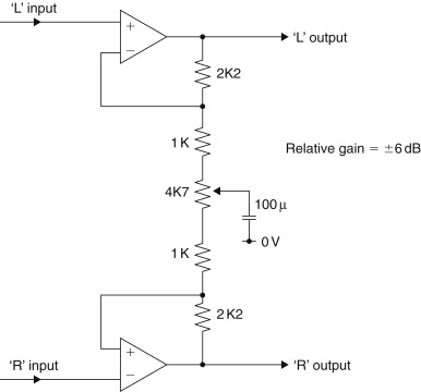
7.18.4. Channel Separation Controls
While the closest reproduction, within the environment of the listener, of the sound stage of the original performance will be given by a certain specific degree of separation between signals within the ‘L’ and ‘R’ channels, it is found that shortcomings in the design of the reproducing and amplifying equipment tend universally to lessen the degree of channel separation rather than the reverse.
Some degree of enhancement of channel separation is therefore often of great value, and electronic circuits for this purpose are available, such as that, due to the author, shown in Figure 7.70.
Figure 7.70. Circuit for producing enhanced or reduced stereo channel separation.

There are also occasions when a deliberate reduction in the channel separation is advantageous, as, for example, in lessening “rumble” effects due to the vertical motion of a poorly engineered record turntable or in lessening the hiss component of a stereo FM broadcast. While this is also provided by the circuit of Figure 7.70, a much less elaborate arrangement, as shown in Figure 7.71, will suffice for this purpose.
Figure 7.71. Simple stereo channel blend control.

A further, and interesting, approach is that offered by Blumlein, who found that an increase or reduction in the channel separation of a stereo signal was given by adjusting the relative magnitudes of the ‘L+R’ and ‘L−R’ signals in a stereo matrix, before these were added or subtracted to give the ‘2L’ and ‘2R’ components.
An electronic circuit for this purpose is shown in Figure 7.72.
Figure 7.72. Channel separation or blending using matrix addition or subtraction.

7.18.5. Filters
While various kinds of filter circuits play a very large part in the studio equipment employed to generate the program material, both as radio broadcasts and as recordings on disc or tape, the only types of filters normally offered to the user are those designed to attenuate very low frequencies, below, say, 50 Hz and generally described as “rumble” filters, or those operating in the region above a few kHz, and generally described as “scratch” or “whistle” filters.
Three such filter circuits are shown in Figure 7.73. Of these, the first two are fixed frequency active filter configurations employing a bootstrap type circuit for use, respectively, in high-pass (rumble) and low-pass (hiss) applications, and the third is an inductor–capacitor passive circuit layout, which allows adjustment of the HF turnover frequency by variation of the capacitor value.
Figure 7.73. Steep-cut filter circuits.

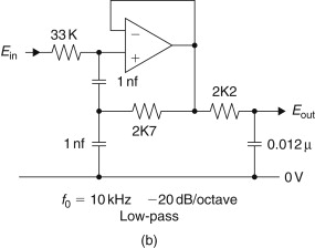

Such frequency adjustments are, of course, also possible with active filter systems, but require the simultaneous switching of a larger number of components. For such filters to be effective in their intended application, the slope of the response curve, as defined as the change in the rate of attenuation as a function of frequency, is normally chosen to be high—at least 20 dB/octave—as shown in Figure 7.74, and, in the case of the filters operating in the treble region, a choice of operating frequencies is often required, as is also, occasionally, the possibility of altering the attenuation rate.
Figure 7.74. Characteristics of circuits of Figures 7.73(a) and 7.73(b).

This is of importance, as rates of attenuation in excess of 6 dB/octave lead to some degree of coloration of the reproduced sound, and the greater the attenuation rate, the more noticeable this coloration becomes. This problem becomes less important as the turnover frequency approaches the limits of the range of human hearing, but very steep rates of attenuation produce distortions in transient waveforms whose major frequency components are much lower than notional cut-off frequency.
It is, perhaps, significant in this context that recent improvements in compact disc players have all been concerned with an increase in the sampling rate, from 44.1 kHz to 88.2 kHz or 176.4 kHz, to allow more gentle filter attenuation rates beyond the 20-kHz audio pass band than that provided by the original 21-kHz “brick wall” filter.
The opinion of the audiophiles seems to be unanimous that such CD players, in which the recorded signal is two or four times “oversampled,” which allows much more gentle “anti-aliasing” filter slopes, have a much preferable HF response and also have a more natural, and less prominent, high-frequency characteristic than that associated with some earlier designs.