
Chapter 13. Noise and Grounding
13.1. Audio Amplifier Printed Circuit Board Design
This section addresses the special printed circuit board (PCB) design problems presented by power amplifiers, particularly those operating in Class-B. All power amplifier systems contain the power-amp stages themselves, and usually associated control and protection circuitry; most also contain small-signal audio sections such as balanced input amplifiers, subsonic filters, output meters, and so on.
Other topics related to PCB design, such as grounding, safety, and reliability, are also dealt with.
The performance of an audio power amplifier depends on many factors, but in all cases the detailed design of the PCB is critical because of the risk of inductive distortion due to cross talk between the supply rails and the signal circuitry; this can very easily be the ultimate limitation on amplifier linearity, and it is hard to overemphasize its importance. The PCB design will, to a great extent, define both the distortion and the cross talk performance of the amplifier.
Apart from these performance considerations, the PCB design can have considerable influence on ease of manufacture, ease of testing and repair, and reliability. All of these issues are addressed here.
Successful audio PCB layout requires enough electronic knowledge to fully appreciate the points set out here so that layout can proceed smoothly and effectively. It is common in many electronic fields for PCB design to be handed over to draftspersons, who, while very skilled in the use of CAD, have little or no understanding of the details of circuit operation. In some fields this works fine; in power amplifier design it will not because basic parameters such as cross talk and distortion are so strongly layout dependent. At the very least the PCB designer should understand the points that follow.
13.1.1. Cross Talk
All cross talk has a transmitting end (which can be at any impedance) and a receiving end, usually either at high impedance or at virtual earth. Either way, it is sensitive to the injection of small currents. When interchannel cross talk is being discussed, the transmitting and receiving channels are usually called speaking and nonspeaking channels, respectively.
Cross talk comes in various forms:
- Capacitative cross talk is a consequence of the physical proximity of different circuits and may be represented by a small notional capacitor joining the two circuits. It usually increases at the rate of 6 dB/octave, although higher dB/octave rates are possible. Screening with any conductive material is a complete cure, but physical distance is usually less expensive.
- Resistive cross talk usually occurs simply because ground tracks have a nonzero resistance. Copper is not a room-temperature superconductor. Resistive cross talk is constant with frequency.
- Inductive cross talk is rarely a problem in general audio design; it might occur if you have to mount two uncanned audio transformers close together, but otherwise you can usually forget it. The notable exception to this rule is the Class-B audio power amplifier, where the rail currents are halfwave sines that seriously degrade the distortion performance if allowed to couple into the input, feedback, or output circuitry.
In most line-level audio circuitry the primary cause of cross talk is unwanted capacitative coupling between different parts of a circuit, and in most cases this is defined solely by the PCB layout. Class-B power amplifiers, in contrast, should suffer very low or negligible levels of cross talk from capacitative effects, as circuit impedances tend to be low and the physical separation large; a much greater problem is inductive coupling between the supply-rail currents and the signal circuitry. If coupling occurs to the same channel, it manifests itself as distortion and can dominate amplifier nonlinearity. If it occurs to the other (nonspeaking) channel it will appear as cross talk of a distorted signal. In either case it is thoroughly undesirable, and precautions must be taken to prevent it.
The PCB layout is only one component of this, as cross talk must be both emitted and received. In general, the emission is greatest from internal wiring due to its length and extent; wiring layout will probably be critical for best performance and needs to be fixed by cable ties, etc. The receiving end is probably the input and feedback circuitry of the amplifier, which will be fixed on the PCB. Designing these sections for maximum immunity is critical to good performance.
13.1.2. Rail Induction Distortion
The supply rails of a Class-B power-amp carry large and very distorted currents. As outlined previously, if these are allowed to cross talk into the audio path by induction, the distortion performance will be severely degraded. This applies to PCB conductors just as much as cabling, and it is sadly true that it is easy to produce an amplifier PCB that is absolutely satisfactory in every respect but this one, and the only solution is another board iteration. The effect can be completely prevented, but in the present state of knowledge I cannot give detailed guidelines to suit every constructional topology. The best approach is to minimize radiation from the supply rails by running the V+ and V− rails as close together as possible. Keep them away from the input stages of the amplifier and the output connections; the best method is to bring the rails up to the output stage from one side, with the rest of the amplifier on the other side. Then run tracks from the output to power the rest of the amp; these carry no halfwave currents and should cause no problems.
Minimize pick-up of rail radiation by keeping the area of the input and feedback circuits to a minimum. These form loops with the audio ground and these loops must be as small in area as possible. This can often best be done by straddling the feedback and input networks across the audio ground track, which is taken across the center of the PCB from input ground to output ground.
Induction of distortion can also occur into the output and output-ground cabling, and even the output inductor. The latter presents a problem as it is usually difficult to change its orientation without a PCB update.
13.1.3. Mounting of Output Devices
The most important decision is whether to mount the power output devices directly on the main amplifier PCB. There are strong arguments for doing so, but it is not always the best choice.
13.1.3.1. Advantages
- The amplifier PCB can be constructed so as to form a complete operational unit that can be tested thoroughly before being fixed into the chassis. This makes testing much easier, as there is access from all sides; it also minimizes the possibility of cosmetic damage (scratches, etc.) to the metalwork during testing.
- It is impossible to connect the power devices wrongly, providing you get the right devices in the right positions. This is important for such errors usually destroy both output devices and cause other domino-effect faults that are very time-consuming to correct.
- The output device connections can be very short. This seems to help stability of the output stage against HF parasitic oscillations.
13.1.3.2. Disadvantages
- If the output devices require frequent changing (which obviously indicates something very wrong somewhere) then repeated resoldering will damage the PCB tracks. However, if the worst happens, the damaged track can usually be bridged out with short sections of wire so that the PCB need not be scrapped; make sure this is possible.
- The output devices will probably get fairly hot, even if run well within their ratings; a case temperature of 90°C is not unusual for a TO3 device. If the mounting method does not have a degree of resilience, then thermal expansion may set up stresses that push the pads off the PCB.
- Because the heat sink will be heavy, there must be a solid structural fixing between this and the PCB. Otherwise the assembly will flex when handled, putting stress on soldered connections.
13.1.4. Single- and Double-Sided Printed Circuit Boards
Because of their lower cost, single-sided PCBs are the usual choice for power amplifiers; however, the price differential between single- and double-sided plated-through-hole (PTH) PCBs is much less than it used to be. It is not usually necessary to go double-sided for reason of space or convoluted connectivity, as power amplifier components tend to be physically large, determining the PCB size, and in typical circuitry there are a large number of discrete resistors, etc., that can be used for jumping tracks.
Bear in mind that single-sided boards need thicker tracks to ensure adhesion in case desoldering is necessary. Adding one or more ears to pads with only one track leading to them gives much better adhesion and is highly recommended for pads that may need resoldering during maintenance; unfortunately, it is a very tedious task with most CAD systems.
The advantages of double-sided PTH for power amplifiers are as follow:
- No links are required.
- Double-sided PCBs may allow one side to be used primarily as a ground plane, minimizing cross talk and EMC problems.
- Much better pad adhesion on resoldering as the pads are retained by the through-hole plating.
- There is more total room for tracks so they can be wider, giving less volt drop and PCB heating.
- The extra cost is small.
13.1.5. Power Supply Printed Circuit Board Layout
Power supply subsystems have special requirements due to the very high capacitor-charging currents involved.
- Tracks carrying the full supply-rail current must have generous widths. The board material used should have not less than 2-oz copper. Four-ounce copper can be obtained but it is expensive and has long lead times; it is not really recommended.
- Reservoir capacitors must have the incoming tracks going directly to the capacitor terminals; likewise the outgoing tracks to the regulator must leave from these terminals. In other words, do not run a tee off to the cap. Failure to observe this puts sharp pulses on the DC and tends to worsen the hum level.
- The tracks to and from the rectifiers carry charging pulses that have a considerably higher peak value than the DC output current. Conductor heating is therefore much greater due to the higher value of I2R. Heating is likely to be especially severe at PC-mount fuse holders. Wire links may also heat up and consideration should be given to two links in parallel; this sounds crude but actually works very effectively.
Track heating can usually be detected simply by examining the state of the solder mask after several hours of full-load operation; the green mask materials currently in use discolor to brown on heating. If this occurs then as a very rough rule the track is too hot. If the discoloration tends to dark brown or black then the heating is serious and must definitely be reduced.
- If there are PCB tracks on the primary side of the mains transformer, and this has multiple taps for multicountry operation, then remember that some of these tracks will carry much greater currents at low voltage tappings; mains current drawn on 90 V input will be nearly three times that at 240 V.
Be sure to observe the standard safety spacing of 60 thou between mains tracks and other conductors for creepage and clearance. (This applies to all track-track, track-PCB edge, and track-metal-fixings spacings.)
In general, PCB tracks carrying mains voltages should be avoided, as presenting an unacceptable safety risk to service personnel. If it must be done, then warnings must be displayed very clearly on both sides of the PCB. Mains-carrying tracks are unacceptable in equipment intended to meet UL regulations in the United States, unless they are fully covered with insulating material that is nonflammable and can withstand at least 120°C (e.g., polycarbonate).
13.1.6. Power Amplifier Printed Circuit Board Layout Details
A simple unregulated supply is assumed.
- Power amplifiers have heavy currents flowing through the circuitry, and all of the requirements for power supply design also apply here. Thick tracks are essential, and 2-oz copper is highly desirable, especially if the layout is cramped.
If attempting to thicken tracks by laying solder on top, remember that ordinary 60:40 solder has a resistivity of about six times that of copper, so even a thick layer may not be very effective.
- The positive and negative rail reservoir caps will be joined together by a thick earth connection; this is called reservoir ground (RG). Do not attempt to use any point on this track as the audio-ground starpoint, as it carries heavy charging pulses and will induce ripple into the signal. Instead, take a thick tee from the center of this track (through which the charging pulses will not flow) and use the end of this as the starpoint.
- Low-value resistors in the output stage are likely to get very hot in operation—possibly up to 200°C. They must be spaced out as much as possible and kept from contact with components such as electrolytic capacitors. Keep them away from sensitive devices such as the driver transistors and the bias-generator transistor.
- Vertical power resistors. The use of these in power amplifiers appears attractive at first because of the small amount of PCB area they take up. However, the vertical construction means that any impact on the component, such as might be received in normal handling, puts a very great strain on the PCB pads, which are likely to be forced off the board. This may result in it being scrapped. Single-sided boards are particularly vulnerable, having much lower pad adhesion due to the absence of vias.
- Solderable metal clips to strengthen the vertical resistors are available in some ranges (e.g., Vitrohm) but this is not a complete solution, and the conclusion must be that horizontal-format power resistors are preferable.
- Rail decoupler capacitors must have a separate ground return to the reservoir ground. This ground must not share any part of the audio ground system, and must not be returned to the starpoint.
- The exact layout of the feedback takeoff point is criticial for proper operation. Usually the output stage has an output rail that connects the emitter power resistors together. This carries the full output current and must be substantial. Take a tee from this track for the output connection and attach the feedback takeoff point to somewhere along this tee. Do not attach it to the track joining the emitter resistors.
- The input stages (usually a differential pair) should be at the other end of the circuitry from the output stage. Never run input tracks close to the output stage. Input stage ground and the ground at the bottom of the feedback network must be the same track running back to the starpoint. No decoupling capacitors may be connected to this track, but it seems to be permissible to connect input bias resistors that pass only very small DC currents.
- Put the input transistors close together. The closer the temperature match, the less the amplifier output DC offset due to Vbe mismatching. If they can both be hidden from seeing the infra-red radiation from the heat sink (e.g., by hiding them behind a large electrolytic), then DC drift is reduced.
- Most power amplifiers will have additional control circuitry for muting relays, thermal protection, etc. Grounds from this must take a separate path back to the reservoir ground, and not the audio starpoint.
- Unlike most audio boards, power amps will contain a mixture of sensitive circuitry and a high-current power supply. Be careful to keep bridge rectifier connections and so on away from input circuitry.
- Mains/chassis ground will need to be connected to the power amplifier at some point. Do not do this at the transformer center tap as this is spaced away from the input ground voltage by the return charging pulses and will create severe ground-loop hum when the input ground is connected to mains ground through another piece of equipment.
Connecting mains ground to starpoint is better, as the charging pulses are excluded, but the track resistance between input ground and star will carry any ground-loop currents and induce a buzz.
Connecting mains ground to the input ground gives maximal immunity against ground loops.
- If capacitors are installed the wrong way round the results are likely to be explosive. Make every possible effort to put all capacitors in the same orientation to allow efficient visual checking. Mark polarity clearly on the PCB, positioned so it is still visible when the component is fitted.
- Drivers and the bias generator are likely to be fitted to small vertical heat sinks. Try to position them so that the transistor numbers are visible.
- All transistor positions should have emitter, base, and collector or whatever marked on the top print to aid fault finding. TO3 devices also need to be identified on the copper side, as any screen printing is covered up when the devices are installed.
- Any wire links should be numbered to make it easier to check that they have all been fitted.
13.1.7. Audio Printed Circuit Board Layout Sequence
PCB layout must be considered from an early stage of amplifier design. For example, if a front-facial layout shows the volume control immediately adjacent to a loudspeaker routing switch, then a satisfactory cross talk performance will be difficult to obtain because of the relatively high impedance of the volume control wipers. Shielding metalwork may be required for satisfactory performance, which adds cost. In many cases the detailed electronic design has an effect on cross talk quite independently from physical layout.
- Consider implications of facia layout for PCB layout.
- Circuitry designed to minimize cross talk. At this stage, try to look ahead to see how op-amp halves, switch sections, and so on should be allocated to keep signals away from sensitive areas. Consider cross talk at above-PCB level; for example, when designing a module made up of two parallel double-sided PCBs, it is desirable to place signal circuitry on the inside faces of the boards, and power and grounds on the outside, to minimize cross talk and maximize RF immunity.
- Facia components (pots, switches, etc.) placed to partly define available board area.
- Other fixed components, such as power devices, driver heat sinks, input and output connectors, and mounting holes placed. The area left remains for the purely electronic parts of the circuitry that do not have to align with metalwork and so may be moved about fairly freely.
- Detailed layout of components in each circuit block, with consideration toward manufacturability.
- Make efficient use of any spare PCB area to fatten grounds and high-current tracks as much as possible. It is not wise to fill in every spare corner of a prototype board with copper as this can be time-consuming (depending on the facilities of your PCB CAD system) and some of it will probably have to be undone to allow modifications.
Ground tracks should always be as thick as practicable. Copper is free.
13.1.8. Miscellaneous Points
- On double-sided PCBs, copper areas should be solid on the component side for minimum resistance and maximum screening, but will need to be cross-hatched on the solder side to prevent distortion if the PCB is flow soldered. A common standard is 10 thou wide noncopper areas, that is, mostly copper with small square holes; this is determined in the CAD package. If in doubt, consult those doing the flow soldering.
- Do not bury component pads in large areas of copper, as this causes soldering difficulties.
- There is often a choice between running two tracks into a pad or taking off a tee so that only one track reaches it. The former is better because it holds the pad more firmly to the board if desoldering is necessary. This is particularly important for components such as transistors that are relatively likely to be replaced; for single-sided PCBs it is absolutely vital.
- If two parallel tracks are likely to cross talk, then it is beneficial to run a grounded screening track between them. However, the improvement is likely to be disappointing, as electrostatic lines of force will curve over the top of the screen track.
- Jumper options must always be clearly labeled. Assume that everyone loses the manual the moment they get it.
- Label pots and switches with their function on the screen-print layer, as this is a great help when testing. If possible, also label circuit blocks, for example, DC offset detect. The labels must be bigger than component ident text to be clearly readable.
13.2. Amplifier Grounding
The grounding system of an amplifier must fulfil several requirements, among which are:
- The definition of a starpoint as the reference for all signal voltages.
- In a stereo amplifier, grounds must be suitably segregated for good cross talk performance. A few inches of wire as a shared ground to the output terminals will probably dominate the cross talk behavior.
- Unwanted AC currents entering the amplifier on the signal ground, due to external ground loops, must be diverted away from the critical signal grounds, that is, the input ground and the ground for the feedback arm. Any voltage difference between these last two grounds appears directly in the output.
- Charging currents for the power supply unit (PSU) reservoir capacitors must be kept out of all other grounds.
Ground is the point of reference for all signals, and it is vital that it is made solid and kept clean; every ground track and wire must be treated as a resistance across which signal currents will cause unwanted voltage drops. The best method is to keep ground currents apart by means of a suitable connection topology, such as a separate ground return to the starpoint for the local HT decoupling, but when this is not practical it is necessary to make every ground track as thick as possible and fattened up with copper at every possible point. It is vital that the ground path has no necks or narrow sections, as it is no stronger than the weakest part. If the ground path changes board side then a single via hole may be insufficient, and several should be connected in parallel. Some CAD systems make this difficult, but there is usually a way to fool them.
Power amplifiers rarely use double-insulated construction and so the chassis and all metalwork must be grounded permanently and solidly for safety. One result of permanent chassis grounding is that an amplifier with unbalanced inputs may appear susceptible to ground loops. One solution is to connect audio ground to chassis only through a 10-Ω resistor, which is large enough to prevent loop currents becoming significant. This is not very satisfactory as:
- The audio system as a whole may not be grounded solidly.
- If the resistor is burnt out due to misconnected speaker outputs, the audio circuitry is floating and could become a safety hazard.
- The RF rejection of the power amplifier is likely to be degraded. A 100-nF capacitor across the resistor may help.
A better approach is to put the audio-chassis ground connection at the input connector so that in Figure 13.1, ground-loop currents must flow through A–B to the protected earth at B and then to mains ground via B–C. They cannot flow through the audio path E–F. This topology is very resistant to ground loops, even with an unbalanced input; the limitation on system performance in the presence of a ground loop is now determined by the voltage drop in the input cable ground, which is outside the control of the amplifier designer. A balanced input could, in theory, cancel out this voltage drop completely.
Figure 13.1. A grounding system for a typical power amplifier.

Figure 13.1 also shows how the other grounding requirements are met. The reservoir charging pulses are confined to the connection D–E and do not flow E–F, as there is no other circuit path. E–F–H carries ripple, etc., from the local HT decouplers, but likewise cannot contaminate the crucial audio ground A–G.
13.3. Ground Loops: How They Work and How to Deal with Them
A ground loop is created whenever two or more pieces of mains-powered equipment are connected together so that mains-derived AC flows through shields and ground conductors, degrading the noise floor of the system. The effect is the worst when two or more units are connected through mains ground as well as audio cabling, and this situation is what is normally meant by the term “ground loop.” However, ground currents can also flow in systems that are not grounded galvanically; they are of lower magnitude but can still degrade the noise floor, so this scenario is also considered here.
Ground currents may either be inherent in the mains supply wiring (see Section 13.3.1) or generated by one or more of the pieces of equipment that make up the audio system (see Sections 13.3.2 and 13.3.3).
Once flowing in the ground wiring, these currents will give rise to voltage drops that introduce hum and buzzing noises. This may occur either in the audio interconnects or inside the equipment itself if it is not well designed.
Here I have used the word “ground” for conductors and so on, whereas “earth” is reserved for the damp crumbly stuff into which copper rods are thrust.
13.3.1. Hum Injection by Mains Grounding Currents
Figure 13.2 shows what happens when a so-called “technical ground,” such as a buried copper rod, is attached to a grounding system that is already connected to “mains ground” at the power distribution board. The latter is mandatory both legally and technically, so one might as well accept this and denote as the reference ground. In many cases this “mains ground” is actually the neutral conductor, which is only grounded at the remote transformer substation. AB is the cable from substation to consumer, which serves many houses from connections tapped off along its length. There is substantial current flowing down the N+E conductor, so point B is often 1 V rms or more above earth. From B onward, in the internal house wiring, neutral and ground are always separate (in the United Kingdom anyway).
Figure 13.2. Pitfalls of adding a “technical ground” to a system that is already grounded via the mains.

Two pieces of audio equipment are connected to this mains wiring at C and D and are joined to each other through an unbalanced cable F–G. Then an ill-advised connection is made to earth at D; the 1-V rms is now impressed on the path B–C–D, and substantial current is likely to flow through it, depending on the total resistance of this path. There will be a voltage drop from C to D, with its magnitude depending on what fraction of the total BCDE resistance is made up by the section C–D. The earth wire C–D will be of at least 1.5 mm2 cross section, and so the extra connection FG down the audio cable is unlikely to reduce the interfering voltage much.
To get a feel for the magnitudes involved, take a plausible ground current of 1 A. The 1.5-mm2 ground conductor will have a resistance of 0.012 Ω/m, so if the mains sockets at C and D are 1 m apart, the voltage C–D will be 12 mV rms. Almost all of this will appear between F and G and will be indistinguishable from wanted signal to the input stage of unit 2, so the hum will be severe, probably only 30 dB below the nominal signal level.
The best way to solve this problem is not to create it in the first place. If some ground current is unavoidable, then the use of balanced inputs (or ground-cancel outputs—it is not necessary to use both) should give at least 40 dB of rejection at audio frequencies.
Figure 13.2 also shows a third earthing point, which fortunately does not complicate the situation. Metal water pipes are bonded to the incoming mains ground for safety reasons, and because they are usually connected electrically to an incoming water supply, current flows through B–W in the same way as it does through the copper rod link D–E. This waterpipe current does not, however, flow through C–D and cannot cause a ground-loop problem. It may, however, cause the pipes to generate an AC magnetic field, which is picked up by other wiring.
13.3.2. Hum Injection by Transformer Stray Magnetic Fields
Figure 13.3 shows a thoroughly bad piece of physical layout that will cause ground currents to flow even if the system is grounded correctly to just one point.
Figure 13.3. A poor cable layout in the PSU at the left wraps a loop around the transformer and induces ground currents.

Here unit 1 has an external DC power supply; this makes it possible to use an inexpensive frame-type transformer, which will have a large stray field. However, note that the wire in the PSU that connects mains ground to the outgoing 0 V takes a half-turn around the transformer, and significant current will be induced into it, which will flow round the loop C–F–G–D, and give an unwanted voltage drop between F and G. In this case, reinforcing the ground of the audio interconnection is likely to be of some help, as it directly reduces the fraction of the total loop voltage that is dropped between F and G.
It is difficult to put any magnitudes to this effect because it depends on many imponderables, such as the build quality of the transformer and the exact physical arrangement of the ground cable in the PSU. If this cable is rerouted to the dotted position in the diagram, the transformer is no longer enclosed in a half-turn, and the effect will be much smaller.
13.3.3. Hum Injection by Transformer Stray Capacitance
It seems at first sight that the adoption of Class II (double-insulated) equipment throughout an audio system will give inherent immunity to ground-loop problems. Life is not so simple, although it has to be said that when such problems do occur they are likely to be much less severe. This problem afflicts all Class II equipment to a certain extent.
Figure 13.4 shows two Class II units connected together by an unbalanced audio cable. The two mains transformers in the units have stray capacitance from both live and neutral to the secondary. If these capacitances were all identical, no current would flow, but in practice they are not, so 50-Hz currents are injected into the internal 0-V rail and flow through the resistance of F–G, adding hum to the signal. A balanced input or ground-canceling output will remove or render negligible the ill effects.
Figure 13.4. The injection of mains current into the ground wiring via transformer interwinding capacitance.

Reducing the resistance of the interconnect ground path is also useful—more so than with other types of ground loop, because the ground current is essentially fixed by the small stray capacitances, and so halving the resistance F–G will dependably halve the interfering voltage. There are limits to how far you can take this; while a simple balanced input will give 40 dB of rejection at low cost, increasing the cross-sectional area of copper in the ground of an audio cable by a factor of 100 times is not going to be either easy or inexpensive. Figure 13.4 shows equipment with metal chassis connected to the 0 V (this is quite acceptable for safety approvals—what counts is the isolation between mains and everything else, not between low-voltage circuitry and touchable metalwork); note that the chassis connection, however, has no relevance to the basic effect, which would still occur even if the equipment enclosure was completely nonconducting.
The magnitude of ground current varies with the details of transformer construction and increases as the size of the transformer grows. Therefore, the more power a unit draws, the larger the ground current it can sustain. This is why many systems are subjectively hum free until the connection of a powered subwoofer, which is likely to have a larger transformer than other components of the system.
| Equipment type | Power consumption | Ground current |
|---|---|---|
| Turntable, CD, cassette deck | 20 W or less | 5 μA |
| Tuners, amplifiers, small TVs | 20–100 W | 100 μA |
| Big amplifiers, subwoofers, large TVs | More than 100 W | 1 mA |
13.3.4. Ground Currents Inside Equipment
Once ground currents have been set flowing, they can degrade system performance in two locations: outside the system units, by flowing in the interconnect grounds, or inside the units, by flowing through internal PCB tracks, etc. The first problem can be dealt with effectively by the use of balanced inputs, but the internal effects of ground currents can be much more severe if the equipment is poorly designed.
Figure 13.5 shows the situation. There is, for whatever reason, ground current flowing through the ground conductor C–D, causing an interfering current to flow round the loop C–F–G–D as before. Now, however, the internal design of unit 2 is such that the ground current flowing through F–G also flows through G–G′ before it encounters the ground wire going to point D. G–G′ is almost certain to be a PCB track with higher resistance than any of the cabling and so the voltage drop across it can be relatively large and the hum performance correspondingly poor. Exactly similar effects can occur at signal outputs; in this case the ground current is flowing through F–F′.
Figure 13.5. If ground current flows through the path F′FGG′, then the relatively high resistance of the PCB tracks produces voltage drops between the internal circuit blocks.

Balanced inputs will have no effect on this; they can cancel out the voltage drop along F–G, but if internal hum is introduced further down the internal signal path, there is nothing they can do about it.
The correct method of handling this is shown in Figure 13.6. The connection to mains ground is made right where the signal grounds leave and enter the units and are made as solidly as possible. The ground current no longer flows through the internal circuitry. It does, however, still flow through the interconnection at F–G, so either a balanced input or a ground-canceling output will be required to deal with this.
Figure 13.6. The correct method of dealing with ground currents; they are diverted away from internal circuitry.

13.3.5. Balanced Mains Power
There has been speculation in recent times as to whether a balanced mains supply is a good idea. This means that instead of live and neutral (230 and 0 V) you have live and the other live (115 V–0–115 V) created by a center-tapped transformer with the tap connected to neutral (see Figure 13.7).
Figure 13.7. Use of a balanced mains supply to cancel ground currents stemming from interwinding capacitance in the mains transformer. This is an expensive solution.
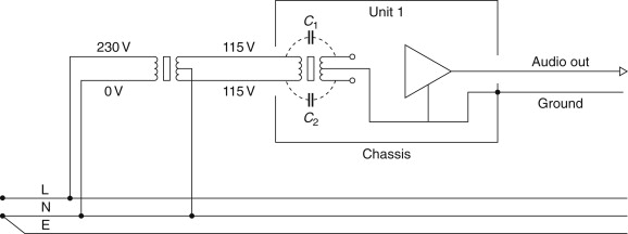
It has been suggested that balanced mains has miraculous effects on sound quality, makes the sound stage ten dimensional, etc. This is obviously nonsense. If a piece of gear is that fussy about its mains (and I do not believe any such gear exists) then dispose of it.
If there is severe radio frequency interference (RFI) on the mains, an extra transformer in the path may tend to filter it out. However, a proper mains RFI filter will almost certainly be more effective—it is designed for the job, after all—and will definitely be less expensive.
Where you might gain a real benefit is in a Class II (i.e., double-insulated) system with very feeble ground connections. Balanced mains would tend to cancel out the ground currents caused by transformer capacitance (see Figure 13.4 and previous discussion for more details on this) and so reduce hum. The effectiveness of this will depend on C1 being equal to C2 in Figure 13.7, which is determined by the details of transformer construction in the unit being powered. I think that the effect would be small with well-designed equipment and reasonably heavy ground conductors in interconnects. Balanced audio connections are a much less expensive and better way of handling this problem, but if none of the equipment has them then beefing up the ground conductors should give an improvement. If the results are not good enough, then, as a last resort, balanced mains may be worth considering.
Finally, bear in mind that any transformer you add must be able to handle the maximum power drawn by the audio system at full throttle. This can mean a large and expensive component.
I would not be certain about the whole of Europe, but to the best of my knowledge it is the same as the United Kingdom, that is, not balanced. The neutral line is at earth potential, give or take a volt, and the live is 230 V above this. The three-phase 11-kV distribution to substations is often described as “balanced” but this just means that power delivered by each phase is kept as near equal as possible for the most efficient use of the cables.
It has often occurred to me that balanced mains 115 V–0–115 V would be a lot safer. Since I am one of those people that put their hands inside live equipment a lot, I do have a kind of personal interest here.
13.4. Class I and Class II
Mains-powered equipment comes in two types: grounded and double insulated. These are officially called Class I and Class II, respectively.
Class I equipment has its external metalwork grounded. Safety against electric shock is provided by limiting the current the live connection can supply with a fuse. Therefore, if a fault causes a short-circuit between live and metalwork, the fuse blows and the metalwork remains at ground potential. A reasonably low resistance in the ground connection is essential to guarantee the fuse blows. A three-core mains lead is mandatory. Two-core IEC mains leads are designed so that they cannot be plugged into three-pin Class I equipment. Class I mains transformers are tested to 1.5 kV rms.
Class II equipment is not grounded. Safety is maintained not by interrupting the supply in case of a fault, but by preventing the fault happening in the first place. Regulations require double insulation and a generally high standard of construction to prevent any possible connection between live and the chassis. A two-core IEC mains lead is mandatory; it is not permitted to sell a three-core lead with a Class II product. This would present no hazard in itself, but is presumably intended to prevent confusion as to what kind of product is in use. Class II mains transformers are tested to 3 kV rms to give greater confidence against insulation breakdown.
Class II is often adopted in an attempt to avoid ground loops. Doing so eliminates the possibility of major problems, at the expense of throwing away all hope of fixing minor ones. There is no way to prevent capacitance currents from the mains transformer flowing through the ground connections (see Section 13.3). It is also no longer possible to put a grounded electrostatic screen between primary and secondary windings. This is serious as it deprives you of your best weapon against mains noise coming in and circuit RF emissions getting out. In Class II the external chassis may be metallic and connected to signal 0 V as often as you like.
If a Class II system is not connected to ground at any point, then the capacitance between primaries and secondaries in the various mains transformers can cause its potential to rise well above ground. If it is touched by a grounded human, then current will flow, and this can sometimes be perceptible, although not directly, as a painful shock such as static electricity. The usual complaint is that the front panel of equipment is “vibrating” or that it feels “furry.” The maximum permitted touch current (flowing to ground through the human body) permitted by current regulations is 700 μA, but currents well below this are perceptible. It is recommended, although not required, that this limit be halved in the tropics where fingers are more likely to be damp. The current is measured through a 50 k resistance to ground.
When planning new equipment, remember that the larger the mains transformer, the greater the capacitance between primary and secondary and the more likely this is to be a problem. To put the magnitudes into perspective, I measured a 500 VA toroid (intended for Class II usage and with no interwinding screen) and found 847 pF between the windings. At 50 Hz and 230 V, this implies a maximum current of 63 μA flowing into the signal circuitry, with the actual figure depending on precisely how the windings are arranged. A much larger 1500 VA toroidal transformer had 1.3 nF between the windings, but this was meant for Class I use and had a screen, which was left floating to get the figure above.
13.4.1. Warning
Please note that the legal requirements for electrical safety are always liable to change. This book does not attempt to give a complete guide to what is required for compliance. The information given here is correct at the time of writing, but it is the designer’s responsibility to check for changes to compliance requirements. The information is given here in good faith but the author accepts no responsibility for loss or damage under any circumstances.
13.5. Mechanical Layout and Design Considerations
The mechanical design adopted depends very much on the intended market and production and tooling resources, but I offer a few purely technical points that need to be taken into account.
13.5.1. Cooling
All power amplifiers will have a heat sink that needs cooling, usually by free convection, and the mechanical design is often arranged around this requirement. There are three main approaches to the problem.
- The heat sink is entirely internal and relies on convected air entering the bottom of the enclosure and leaving near the top (passive cooling).
13.5.1.1. Advantages
The heat sink may be connected to any voltage, which may eliminate the need for thermal washers between power device and sink. However, some sort of conformal material is still needed between transistor and heat sink. A thermal washer is much easier to handle than the traditional white oxide-filled silicone compound, so you will be using them anyway. There are no safety issues as to heat sink temperatures.
13.5.1.2. Disadvantages
Because of the limited fin area possible inside a normal-sized box and the relatively restricted convection path, this system is not suitable for large dissipations.
- The heat sink is partly internal and partly external, as it forms one or more sides of the enclosure. Advantages and disadvantages are much as just described; if any part of the heat sink can be touched, then the restrictions on temperature and voltage apply. Greater heat dissipation is possible.
- The heat sink is primarily internal, but is fan cooled (active cooling). Fans always create some noise, which increases with the amount of air they are asked to move. Fan noise is most unwelcome in a domestic hi-fi environment, but is of little importance in PA applications. This allows maximal heat dissipation, but requires an inlet filter to prevent the build-up of dust and fluff internally. Persuading people to clean such filters regularly is near impossible.
Efficient passive heat removal requires extensive heat sinking with a free convective air flow, and this indicates putting the sinks on the side of the amplifier; the front will carry at least the mains switch and power indicator light, while the back carries the in/out and mains connectors so that only the sides are completely free.
The internal space in the enclosure will require some ventilation to prevent heat build-up; slots or small holes are desirable to keep foreign bodies out. Avoid openings on the top surface as these will allow the entry of spilled liquids and increase dust entry. BS415 is a good starting point for this sort of safety consideration, and this specifies that slots should be no more than 3 mm wide.
Reservoir electrolytics, unlike most capacitors, suffer significant internal heating due to ripple current. Because the electrolytic capacitor life is very sensitive to temperature, mount them in the coolest position available and, if possible, leave room for air to circulate between them to minimize the temperature rise.
13.5.2. Convection Cooling
It is important to realize that the buoyancy forces that drive natural convection are very small and that even small obstructions to flow can seriously reduce the rate of flow, and hence the cooling. If ventilation is by slots in the top and bottom of an amplifier case, then the air must be drawn under the unit and then execute a sharp right-angle turn to go up through the bottom slots. This change of direction is a major impediment to air flow, and if you are planning to lose a lot of heat then it feeds into the design of something so humble as the feet the unit stands on; the higher the better for air flow. In one instance the amplifier feet were made 13 mm taller and all the internal amplifier temperatures dropped by 5°C. Standing such a unit on a thick-pile carpet can be a really bad idea, but someone is bound to do it (and then drop their coat on top of it); hence the need for overtemperature cutouts if amplifiers are to be fully protected.
13.5.3. Mains Transformers
A toroidal transformer is useful because of its low external field. It must be mounted so that it can be rotated to minimize the effect of what stray fields it does emit. Most suitable toroids have single-strand secondary leadouts, which are too stiff to allow rotation; these can be cut short and connected to suitably large flexible wire such as 32/02, with carefully sleeved and insulated joints. One prototype amplifier I have built had a sizeable toroid mounted immediately adjacent to the TO3 end of the amplifier PCB; however, complete cancellation of magnetic hum (hum and ripple output level below 290 dBu) was possible on rotation of the transformer.
A more difficult problem is magnetic radiation caused by reservoir charging pulses (as opposed to the ordinary magnetization of the core, which would be essentially the same if the load current was sinusoidal), which can be picked up by either the output connections or cabling to the power transistors if these are mounted off board. For this reason, the transformer should be kept physically as far away as possible from even the high-current section of the amplifier PCB.
As usual with toroids, ensure that the bolt through the middle cannot form a shorted turn by contacting the chassis in two places.
13.5.4. Wiring Layout
There are several important points about the wiring for any power amplifier:
- Keep the+and 2 HT supply wires to the amplifiers close together. This minimizes the generation of distorted magnetic fields that may otherwise couple into the signal wiring and degrade linearity. Sometimes it seems more effective to include the 0-V line in this cable run; if so, it should be tightly braided to keep the wires in close proximity. For the same reason, if the power transistors are mounted off the PCB, the cabling to each device should be configured to minimize loop formation.
- The rectifier connections should go directly to the reservoir capacitor terminals and then away again to the amplifiers. Common impedance in these connections superimposes charging pulses on the rail ripple waveform, which may degrade amplifier PSRR.
- Do not use the actual connection between the two reservoir capacitors as any form of starpoint. It carries heavy capacitor-charging pulses that generate a significant voltage drop even if thick wire is used. As Figure 13.1 shows, the starpoint is teed off from this connection. This is a starpoint only insofar as the amplifier ground connections split off from here, so do not connect the input grounds to it, as distortion performance will suffer.
13.5.5. Semiconductor Installation
- Driver transistor installation. These are usually mounted onto separate heat sinks that are light enough to be soldered into the PCB without further fixing. Silicone thermal washers ensure good thermal contact, and spring clips are used to hold the package firmly against the sink. Electrical isolation between device and heat sink is not normally essential, as the PCB need not make any connection to the heat sink fixing pads.
- TO3P power transistor installation. These large flat plastic devices are usually mounted on to the main heat sink with spring clips, which are not only rapid to install, but also generate less mechanical stress in the package than bolting the device down by its mounting hole. They also give a more uniform pressure onto the thermal washer material.
- TO3 power transistor installation. The TO3 package is extremely efficient at heat transfer, but notably more awkward to mount.
My preference is for TO3s to be mounted on an aluminium thermal coupler bolted against the component side of the PCB. The TO3 pins may then be soldered directly on the PCB solder side. The thermal coupler is drilled with suitable holes to allow M3.5 fixing bolts to pass through the TO3 flange holes, through the flange, and then be secured on the other side of the PCB by nuts and crinkle washers, which will ensure good contact with the PCB mounting pads. For reliability, the crinkle washers must cut through the solder tinning into the underlying copper; a solder contact alone will creep under pressure and the contact force will decay over time.
Insulating sleeves are essential around the fixing bolts where they pass through the thermal coupler; nylon is a good material for these as it has a good high-temperature capability. Depending on the size of the holes drilled in the thermal coupler for the two TO3 package pins (and this should be as small as practicable to maximize the area for heat transfer), these are also likely to require insulation; silicone rubber sleeving carefully cut to length is very suitable.
An insulating thermal washer must be used between TO3 and flange; these tend to be delicate and the bolts must not be overtightened. If you have a torque wrench, then 10 Nw/m is an approximate upper limit for M3.5 fixing bolts. Do not solder the two transistor pins to the PCB until the TO3 is mounted firmly and correctly, fully bolted down, and checked for electrical isolation from the heat sink. Soldering these pins and then tightening the fixing bolts is likely to force the pads from the PCB. If this should happen, then it is quite in order to repair the relevant track or pad with a small length of stranded wire to the pin; 7/02 size is suitable for a very short run.
Alternatively, TO3s can be mounted off PCB (e.g., if you already have a large heat sink with TO3 drillings) with wires taken from the TO3 pads on the PCB to the remote devices. These wires should be fastened together (two bunches of three is fine) to prevent loop formation; see earlier discussion. I cannot give a maximum safe length for such cabling, but certainly 8 inches causes no HF stability problems. The emitter and collector wires should be substantial, for example, 32/02, but the base connections can be as thin as 7/02.