
Chapter 9. Audio Amplifiers
Solid-state device technologies, which are available to the amplifier designer, fall, broadly, into three categories: bipolar junction transistors (BJTs) and junction diodes; junction field effect transistors (FETs); and insulated gate FETs, usually referred to as MOSFETs (metal oxide silicon FETs), because of their method of construction. These devices are available in both P type—operating from a negative supply line—and N type—operating from a positive supply line. BJTs and MOSFETs are also available in small-signal and larger power versions, whereas FETs and MOSFETs are manufactured in both enhancement-mode and depletion-mode forms. Predictably, this allows the contemporary circuit designer very considerable scope for circuit innovation, by comparison with electronic engineers of the past, for whom there was only a very limited range of vacuum tube devices.
In addition, there is a very wide range of integrated circuits (ICs), which are complete functional modules in some (usually quite small) individual packages. These are designed both for general-purpose use, such as operational amplifiers, and for more specific applications, such as voltage regulator devices, current mirrors, current sources, phase-sensitive rectifiers, and an enormous variety of designs for digital applications, which mostly lie outside the scope of this book.
In the case of discrete devices, I think it is unnecessary for the purposes of audio amplifier design to understand the physical mechanisms by which the devices work, provided that their would-be user has a reasonable grasp of their operating characteristics and limitations and, above all, a knowledge of just what is available.
9.1. Junction Transistors
These are nearly always three-layer devices, fabricated by the multiple and simultaneous vapor phase diffusion and etching of small and intricate patterns on a large, thin slice of very high purity single crystal silicon. A few devices are still made in germanium, mainly for replacement purposes, and some VHF components are made in gallium arsenide, but these will not, in general, lie within the scope of this book. The fabrication techniques may be based on the use of a completely undoped (intrinsic) slice of silicon, into which carefully controlled quantities of impurities are diffused through an appropriate mask pattern from both sides of the slice. These are described in the manufacturers’ literature as double diffused, triple diffused, and so on.
In a later technique, evolved by the Fairchild Instrument Corporation, all the diffusions were made from one side of the slice. These devices were called planar and had, normally, a better HF response and more precisely controlled characteristics than, for example, equivalent double-diffused devices. In a further, more recent, technique, also due to Fairchild, the silicon slice will have been made to grow a surface layer of uniformly doped silicon on the exposed side (which will usually form the base region of a transistor) and a single diffusion was then made into this doped layer to form the emitter junction. This technique was called epitaxial and led to transistors with superior characteristics, especially at HF. Since this is the least expensive BJT fabrication process, it will normally be used wherever it is practicable, and if no process is specified it may reasonably be supposed to be a planar-epitaxial type.
In contrast to a thermionic valve, which is a voltage-controlled device, the BJT is a current operated one. So while a change in the base voltage will result in a change in the collector current, this has a very nonlinear relationship to the applied base voltage. In comparison to this, the collector current changes with the input current to the base in a relatively linear manner. Unfortunately, this linear relationship between Ic and Ib tends to deteriorate at higher base current levels, as shown in Figure 9.1. This relationship between base and collector currents is called the current gain, and for AC operation is given the term hfe, and its nonlinearity is an obvious source of distortion when the device is used as an amplifier. Alternatively, one could regard this lack of linearity as a change of hFE (this term is used to define the DC or LF characteristics of the device) as the base current is changed. A further problem of a similar kind is the change in hfe as a function of signal frequency, as shown in Figure 9.2.
Figure 9.1. BJT nonlinearity.

Figure 9.2. Decrease in hfe with frequency.

However, as a current amplifier (which generally implies operation from a high impedance signal source) the behavior of a BJT is vastly more linear than when used as a voltage amplifying stage, for which the input voltage/output current relationships are shown for an NPN silicon transistor as line ‘a’ in Figure 9.3. (I have included, as line ‘b’, for reference, the comparable characteristics for a germanium junction transistor, although this would normally be a PNP device with a negative base voltage, and a negative collector voltage supply line.) By comparison with, say, a triode valve, whose anode current/grid voltage relationships are also shown as line ‘c’ in Figure 9.3, the BJT is a grossly nonlinear amplifying device, even if some input (positive in the case of an NPN device) DC bias voltage has been chosen so that the transistor operates on a part of the curve away from the nonconducting initial region.
Figure 9.3. Comparative characteristics of valve, germanium, and silicon based BJTs.

9.2. Control of Operating Bias
There are three basic ways of providing a DC quiescent voltage bias to a BJT, which is shown in Figure 9.4. In the first of these methods, shown in Figure 9.4(a), an arrangement that is fortunately seldom used, the method adopted is simply to connect an input resistor, R1, between the base of the transistor and some suitable voltage source. This voltage can then be adjusted so that the collector current of the transistor is of the right order to place the collector potential near its desired operating voltage. The snag with this scheme is that transistors vary quite a lot from one to another of nominally the same type, so this would require to be set anew for each individual device. Also, if the operating temperature changes, the current gain of the device (which is temperature sensitive) will be altered and, with it, the collector current of Q1 and its working potential. The arrangement shown in Figure 9.4(b) is somewhat preferable in that a high current gain transistor, or one working at a higher temperature, will pass more current, and this will lower the collector voltage of Q1, which will, in turn, reduce the bias current flowing through R1. However, this also provides NFB and will limit the stage gain to a value somewhat less than R1/Zin.
Figure 9.4. Biasing circuits.


The method almost invariably used in competently designed circuitry is that shown in Figure 9.4(c), or some equivalent layout. In this, a potential divider (R1,R2) having an output impedance low in relation to the base impedance of Q1 is used to provide a fixed DC base potential. Since the emitter will, by emitter–follower action, sit at a potential, depending on emitter current, which is about 0.6 V below that of the base, the value of R4 will then determine the emitter and collector currents, and the operating conditions so provided will hold good for almost any broadly similar device used in this position. Since the emitter resistor would cause a significant reduction in stage gain, as seen in the equivalent analysis of valve cathode bias systems, it is customary to bypass this resistor with a capacitor, C2, which is chosen to have an impedance low in relation to R4 and R3.
9.3. Stage Gain
The stage gain of a BJT, used as a simple amplifier, can be determined from the relationship:
![]() where Rs is the source resistance, RL is the collector load resistor, hfe is the small-signal (AC) current gain, and ri is the internal emitter-base resistance of the transistor. An alternative and somewhat simpler approach is similar to that
used for a pentode valve gain stage in which
where Rs is the source resistance, RL is the collector load resistor, hfe is the small-signal (AC) current gain, and ri is the internal emitter-base resistance of the transistor. An alternative and somewhat simpler approach is similar to that
used for a pentode valve gain stage in which
![]() where the gm of a typical modern planar epitaxial silicon transistor will be in the range of 25–40 mS/mA of collector current. Because
the gm of the junction transistor is so high, high stage gains can be obtained with a relatively low value of load resistor. For
example, a small-signal transistor with a supply voltage of 15 V, a 4 k7 collector load resistor, and a collector current
of 2 mA will have a low frequency stage gain, for a relatively low source resistance, of some 300˘. If some way can be found
for increasing the load impedance, without also increasing the voltage drop across the load, very high gains indeed can be
achieved—up to 2500 with a junction FET acting as a high impedance constant current load.1
where the gm of a typical modern planar epitaxial silicon transistor will be in the range of 25–40 mS/mA of collector current. Because
the gm of the junction transistor is so high, high stage gains can be obtained with a relatively low value of load resistor. For
example, a small-signal transistor with a supply voltage of 15 V, a 4 k7 collector load resistor, and a collector current
of 2 mA will have a low frequency stage gain, for a relatively low source resistance, of some 300˘. If some way can be found
for increasing the load impedance, without also increasing the voltage drop across the load, very high gains indeed can be
achieved—up to 2500 with a junction FET acting as a high impedance constant current load.1
A predictable, but interesting aspect of stage gain is that the higher the gain, which can be obtained from a circuit module, the lower the distortion in this which will be due to the input device. This is so because if increasingly small segments are taken from any curve, they will progressively approach more closely to a straight line in their form. This allows a very low THD figure, much less than 0.01% at 2 V rms output, over the frequency range 10 Hz–20 kHz, to be obtained from the simple NPN/PNP feedback pair shown in Figure 9.5, which would have an open loop gain of several thousand. The distortion contributed by Q2 will be relatively low because of the high effective source resistance seen by the Q2 base. A similar low level of distortion is given by the amplifier layout (bipolar transistor with constant current load) described earlier because of the very high stage gain of the amplifying transistor and the consequent utilization of only a very small portion of its Ic/Vb curve.
Figure 9.5. NPN/PNP feedback pair.

9.4. Basic Junction Transistor Circuit Configurations
As in the case of the thermionic valve, there are a number of layouts, in addition to the simple single transistor amplifier shown in Figure 9.4 or the two-stage amplifier of Figure 9.5, that can be used to provide a voltage gain or to perform an impedance transformation function. There is, for example, the grounded base layout of Figure 9.6, which has a very low input impedance, a high output impedance, and a very good HF response. This circuit is far from being only of academic interest in the audio field in that it can provide, for example, a very effective low input impedance amplifier circuit for a moving coil pick-up cartridge. I showed a circuit of this type, dating from about 1980, in an earlier book (Audio Electronics, Newnes, 1995, p. 133).
Figure 9.6. Grounded base stage.

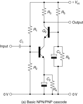
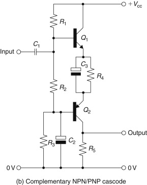
The cascode layout is also used very widely as a voltage amplifier stage, using a circuit arrangement of the kind shown in Figure 9.7(a). As in the case of the valve amplifier stage, this circuit gives very good input/output isolation and an excellent HF performance due to its freedom from capacitative feedback from output to input. It can also be rearranged, as shown in Figure 9.7(b), so that the input stage acts as an emitter–follower, which gives a very high input impedance.
Figure 9.7. Cascode layouts.
The long-tailed pair layout, shown in its simplest form in Figure 9.8(a), gives a very good input/output isolation; also, because it is of its nature a push–pull layout, it gives a measure of reduction in even-order harmonic distortion. Its principal advantage, and the reason why this layout is normally used, is that it allows, if the tail resistor (R1) is returned to a –ve supply rail, both of the input signal ports to be referenced to the 0-V line—a feature that is enormously valuable in DC amplifying systems. The designer may sometimes seek to improve the performance of the circuit block by using a high impedance (active) tail in place of a simple resistor, as shown in Figure 9.8(b). This will lessen the likelihood of unwanted signal breakthrough from the –ve supply rail, as well as ensuring a greater degree of dynamic balance, and signal transfer, between the two halves.
Figure 9.8. Long-tailed pair layouts.


Although like all solid-state amplifying systems it is free from the bugbears of hum and noise intrusion from the heater supply of a valve amplifying stage—likely in any valve amplifier where there is a high impedance between cathode and ground—it is less good from the point of view of thermal noise than a similar single stage amplifier, partly because there is an additional device in the signal line and partly because the gain of a long-tailed pair layout will only be half that of a comparable single device gain stage. This arises because if a voltage increment is applied to the base of Q1, then the Q1 emitter will only rise half of that amount due to the constraint from Q2, which will also see, but in opposite phase and halved in size, the same voltage increment. This allows, as in the case of the valve phase splitter, a very close similarity, but in opposite phase, of the output currents at Q1 and Q2 collectors.
9.5. Emitter–Follower Systems
These are the solid-state equivalent of the valve cathode follower layout, although offering superior performance and greater versatility. In the simple circuit shown in Figure 9.9 (the case shown is for an NPN transistor, but a virtually identical circuit, but with negative supply rails, could be made with a similar PNP transistor), the emitter will sit at a quiescent potential about 0.6 V more negative than that of the base, and this will follow, quite accurately, any signal voltage excursions applied to the base. (There are some caveats in respect of capacitative loads; these potential problems will be explored under the heading of slew rate limiting.) The output impedance of this circuit is low because this is approximately equal to 1/gm, and the gm of a typical small-signal, silicon BJT is of the order of 35 mA/V (35 mS) per mA of emitter current. So, if Q1 is operated at 5 mA, the expected output impedance, at low frequencies, will be 1/(5.35) kilohms, or 5.7 ohms, a value that is sufficiently smaller than any likely value for R1, that the presence of this resistor will not greatly affect the output impedance of the circuit.
Figure 9.9. Emitter–follower.

The output impedance of a simple emitter–follower can be reduced still further by the circuit elaboration shown in Figure 9.10, known as a compound emitter–follower. In this, the output impedance is lowered in proportion to the effective current gain of Q2 in that, by analogy with the output impedance of an operational amplifier with overall NFB, any change in the potential of the Q1 emitter, brought about by an externally impressed voltage, will result in an opposing change in the collector current of Q2. This layout gives a comparable result to that of the Darlington pair, of two transistors, in cascade, connected as emitter–followers, shown in Figure 9.11, except that the arrangement of Figure 9.10 will only have an input/output DC offset equivalent to a single emitter-base forward voltage drop, whereas the layout of Figure 9.11 will have two, giving a combined quiescent voltage offset of the order of 1.3–1.5 V. Nevertheless, in commercial terms, the popularity of power transistors, connected internally as a Darlington pair, mainly for use in the output stages of audio amplifiers, is great enough for a range of single chip Darlington devices to be offered by the semiconductor manufacturers.
Figure 9.10. Compound emitter–follower.
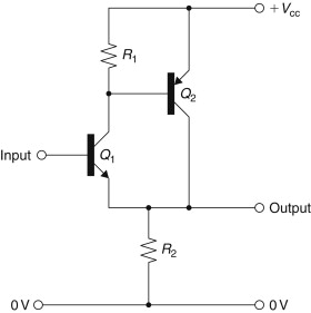
Figure 9.11. Darlington pair.

9.6. Thermal Dissipation Limits
Unlike a thermionic valve, the active area of a BJT is very small, in the range of 0.5 mm for a small signal device to 4 mmor more for a power transistor. Because the physical area of the component is so small—this is a quite deliberate choice on the part of the manufacturer because it reduces the individual component cost by allowing a very large number of components to be fabricated on a single monocrystalline silicon slice—the slice thickness must also be kept as small as possible—values of 0.15–0.5 mm are typical—in order to assist the conduction of any heat evolved by the transistor action away from the collector junction to the metallic header on which the device is mounted.
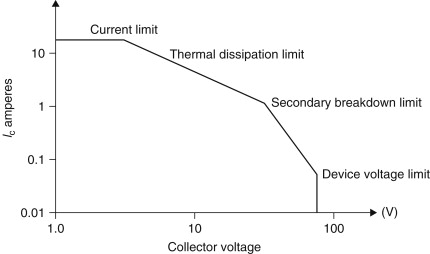
Whereas in a valve, in which the internal electrode structure is quite massive and heat is lost by a combination of radiation and convection, the problem of overheating is usually the unwanted release of gases trapped in its internal metalwork, the problem in a BJT is the phenomenon known as thermal runaway. This can happen because the potential barrier of a P-N junction (that voltage that must be exceeded before current will flow in the forward direction) is temperature dependent and decreases with temperature. Because there will be unavoidable nonuniformities in the doping levels across the junction, this will lead to nonuniform current flow through the junction sandwich, with the greatest flow taking place through the hottest region. If the ability of the device to conduct heat away from the junction is inadequate to prevent the junction temperature rising above permissible levels, this process can become cumulative. This will result in the total current flow through the device being funneled through some very small area of the junction, which may permanently damage the transistor. This malfunction is termed secondary breakdown, and the operating limits imposed by the need to avoid this failure mechanism are shown in Figure 9.12. Field effect devices do not suffer from this type of failure.
Figure 9.12. Bipolar breakdown limits.
9.7. Junction Field Effect Transistors (JFETs)
JFETs are, almost invariably, depletion mode devices, which means that there will be some drain current at a zero-applied gate-source potential. This current will decrease in a fairly linear manner as the reverse gate-source potential is increased, giving an operating characteristic, which is, in the case of an N-channel JFET, very similar to that of a triode valve, as shown in curve ‘c’ of Figure 9.3. Like a thermionic valve, the operation of the device is limited to the range between drain (or anode) current cutoff and gate (or grid) current. In the case of the JFET, this is because the gate-channel junction is effectively a silicon junction diode—normally operated under reverse bias conditions. If the gate source voltage exceeds some 0.6 V in the forward direction, it will conduct, which will prevent gate voltage control of the channel current.
P-channel JFETs are also made, although in a more limited range of types, and these have what is virtually a mirror image of the characteristics of their N-channel equivalents, although in this case the gate-source forward conduction voltage will be of the order of −0.6 V, and drain current cutoff will occur in the gate voltage range of +3 to +8 V. Although Sony did introduce a range of junction FETs for power applications, these are no longer available, and typical contemporary JFETs cover the voltage range (maximum) from 15 to 50 V, mainly limited by the gate-drain reverse breakdown potential, and with permitted dissipations in the range 250–400 mW. Typical values of gm (usually called gfs in the case of JFETs) fall in the range of 2–6 mS.
JFETs mainly have good high-frequency characteristics, particularly the N-channel types, of which there are some designs capable of use up to 500 MHz. Modern types can also offer very low noise characteristics, although their very high input impedance will lead to high values of thermal noise if their input circuitry is also of high impedance; however, this is within the control of the circuit designer. The internal noise resistance of a JFET, R(n), is related to the gfs of the device by
![]() and the value of gfs can be made higher by paralleling a number of channels within the chip. The Hitachi 2SK389 dual matched-pair JFET achieves
a gfs value of 20 mS by this technique, with an equivalent channel thermal noise resistance of 33 ohms.2
and the value of gfs can be made higher by paralleling a number of channels within the chip. The Hitachi 2SK389 dual matched-pair JFET achieves
a gfs value of 20 mS by this technique, with an equivalent channel thermal noise resistance of 33 ohms.2
Although JFETs will work in most of the circuit layouts shown for junction transistors, the most significant difference in the circuit structure is due to their different biasing needs. In the case of a depletion mode device it is possible to use a simple source bias arrangement, similar to the cathode bias used with an indirectly heated valve, of the kind shown in Figure 9.13. As before, the source resistor, R3, will need to be bypassed with a capacitor, C2, if the loss of stage gain due to local NFB is to be avoided. As with a pentode valve, which the junction FET greatly resembles in its operational characteristics, the simplest way of calculating stage gain is by the relationship:
![]()
Figure 9.13. Simple JFET biasing system.

The device manufacturers will frequently modify the structure of the JFET to linearize its Vg/Id characteristics, but, in an ideal device, these will have a square-law relationship, as defined by
![]()
For a typical JFET operating at 2 mA drain current, the gfs value will be of the order of 1–4 mS, which would give a stage gain of up to 40 if R2, in Figure 9.13, is 10 kΩ This is very much lower than would be given by a BJT and is the main reason why they are not often used as voltage-amplifying devices in audio systems unless their very high input impedance (typical values are of the order of 1012 Ω) or their high, and largely constant, drain impedance characteristics are advantageous.
The real value of the JFET emerges in its use with other devices, such as the bipolar/FET cascode shown in Figure 9.14 or the FET/FET cascode layout of Figure 9.15. In the first of these, use of the JFET in the cascode connection confers the very high output impedance of the JFET and the high degree of output/input isolation characteristic of the cascode layout, coupled with the high stage gain of the BJT. The source potential of the JFET (Q2) will be determined by the reverse bias appearing across the source/gate junction, and could typically be of the order of 2–5 V, which will define the collector potential applied to Q1. A further common application of this type of layout is that in which the cascode FET (Q2 in Figure 9.15) is replaced by a high-voltage BJT. The purpose of this arrangement is to allow a JFET amplifier stage to operate at a much higher rail voltage than would be allowable to the FET on its own; this layout is often found as the input stage of high-quality audio amps.
Figure 9.14. Bipolar/FET cascode.

Figure 9.15. FET/FET cascode.

A feature that is very characteristic of the JFET is that for drain potentials above about 3 V, the drain current for a given gate voltage is almost independent of the drain voltage, as shown in Figure 9.16. BJTs have a high characteristic collector impedance, but their Ic/Vc curve for a fixed base voltage, also shown, for comparison, in Figure 9.16, is not as flat as that of the JFET. The very high dynamic impedance of the JFET resulting from this very flat Id/Vd relationship encourages the use of these devices as constant current sources, shown in Figure 9.17. In this form the JFET can be treated as a true two-terminal device, from which the output current can be adjusted, with a suitable JFET, over the range of several milliamperes down to a few microamperes by means of RV1.
Figure 9.16. Drain current characteristics of junction FET.

Figure 9.17. Current source layout.

9.8. Insulated Gate FETs (MOSFETs)
Insulated gate FET devices, usually called MOSFETs, are by far the most widely available, and most widely used, of all the field effect transistors. They normally have a rather worse noise figure than an equivalent JFET, but, on the plus side, they have rather more closely controlled operating characteristics. The range of types available covers the very small-signal, low-working voltage components used for VHF amplification in TVs and FM tuners (for which applications a depletion-mode dual-gate device has been introduced that has very similar characteristics to those of an RF pentode valve) to high-power, high-working voltage devices for use in the output stages of audio amplifiers, as well as many other high-power and industrial applications. They are made in both depletion- and enhancement-mode forms (the former having gate characteristics similar to that of the JFET, whereas the latter description refers to the style of device in which there is normally no drain current in the absence of any forward gate bias), in N-channel and P-channel versions, and, at the present time, in voltage and dissipation ratings of up to 1000 V and 600 W, respectively.
All MOSFETs operate in the same manner, in which a conducting electrode (the gate) situated in proximity to an undoped layer of very high purity single-crystal silicon (the channel), but separated from it by a very thin insulating layer, is caused to induce an electrostatic charge in the channel, which will take the form of a layer of mobile electrons or holes. In small-signal devices this channel is formed on the surface of the chip between two relatively heavily doped regions, which will act, respectively, as the source and the drain of the FET, while the conducting electrode will act as the current controlling gate.
Although modern photolithographic techniques are capable of generating exceedingly precise diffusion patterns, the length of the channel formed by surface-masking techniques in a lateral MOSFET will be too long to allow a low channel “on” resistance. For high current applications, the semiconductor manufacturers have therefore evolved a range of vertical MOSFETs. In these, very short channel lengths are achieved by sequential diffusion processes from the surface, which are then followed by etching a V- or U-shaped trough inward from the surface so that the active channel is formed across the exposed edge of a thin diffused region. Because this channel is short in length, its resistance will be low, and because the manufacturers generally adopt device structures that allow a multiplicity of channels to be connected electrically in parallel, channel “on” resistances as low as 0.008 Ω have been achieved.
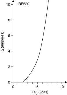
Like a JFET, the MOSFET would, left to itself, have a square-law relationship between gate voltage and drain current. However, in practice, this is affected by the device geometry, and many modern devices have a quite linear Id/Vg characteristic, as shown in Figure 9.18 for an IRF520 power MOSFET.
Figure 9.18. Power MOSFET.
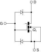
The basic problem with the MOSFET is that of gate/channel overvoltage breakdown, in which the thin insulating layer of silicon oxide or silicon nitride between the gate electrode and the channel breaks down. If this happens the gate voltage will no longer control the drain current and the device is defunct. Because it is theoretically possible for an inadvertent electrostatic charge, such as might arise with respect to the ground if a user were to wear nylon or polyester fabric clothing and well-insulated shoes, it is common practice in the case of small-signal MOSFETs for protective diodes to be formed on the chip at the time of manufacture. These could be either zener diodes or simple junction diodes connected between the gate and the source or the source and drain, as shown in Figure 9.19.
Figure 9.19. Diode gate protection.
In power MOSFETs, these protective devices are seldom incorporated into the chip. There are two reasons for this: (1) that the effective gate/channel area is so large that the associated capacitance is high, which would then require a relatively large inadvertently applied static charge to generate a destructive gate/channel voltage (typically >40 V), and (2) that such protective diodes could, if they were triggered into conduction, cause the MOSFET to act as a four-layer thyristor and become an effective electrical short circuit. However, there are usually no performance penalties that will be incurred by connecting some external protective zener diode in the circuit to prevent the gate/source or gate/drain voltage exceeding some safe value; this is a common feature in the output stages of audio power amplifiers using MOSFETs.
Apart from the possibility of gate breakdown, which, in power MOSFETs, always occurs at less than the maker’s quoted voltage, except at zero drain current, MOSFETs are quite robust devices, and the safe operating area rating (SOAR) curve of these devices, shown for a typical MOSFET in Figure 9.20, is free from the threat of secondary breakdown whose limits are shown, for a power BJT, in Figure 9.12. The reason for this freedom from localized thermal breakdown in the MOSFET is that the mobility of the electrons (or holes) in the channel decreases as the temperature increases, which gives all FETs a positive temperature coefficient of channel resistance.
Figure 9.20. Power MOSFET SOAR limits.

Although it is possible to propose a mathematical relationship between gate voltage and drain current, with MOSFETs as was done in the case of the JFET, the manufacturers tend to manipulate the diffusion pattern and construction of the device to linearize its operation, which leads to the type of performance (quoted for an actual device) shown in Figure 9.21. However, as a general rule, the gfs of a MOSFET will increase with drain current, and a forward transconductance (slope) of 10 S/A is quoted for an IRF140 at an ID value of 15 A.
Figure 9.21. MOSFET characteristics.

9.9. Power BJTs vs Power MOSFETs as Amplifier Output Devices
Some rivalry appears to have arisen between audio amplifier designers over the relative merits of power BJTs, as compared with power MOSFETs. Predictably, this is a mixture of advantages and drawbacks. Because of the much more elaborate construction of the MOSFET, in which a multiplicity of parallel connected conducting channels is fabricated to reduce the conducting “on” resistance, the chip size is larger and the device is several times more expensive both to produce and to buy. The excellent HF characteristics of the MOSFET, especially the N-channel V and U MOS types, can lead to unexpected forms of VHF instability, which can, in the hands of an unwary amplifier designer, lead to the rapid destruction of the output devices. However, this excellent HF performance, when handled properly, makes it much easier to design power amplifiers with good gain and phase margins in the feedback loop, where overall NFB is employed. In contrast, the relatively sluggish and complex characteristics of the junction power transistor can lead to difficulties in the design of feedback amplifiers with good stability margins.
Also, as has been noted, the power MOSFET is intrinsically free from the problem of secondary breakdown, and an amplifier based on these does not need the protective circuitry that is essential in amplifiers with BJT output devices if failure is to be avoided when they are used at high power levels with very low impedance or reactive loads. The problem here is that the protective circuitry may cut in during high-frequency signal level peaks during the normal use of the amplifier, which can lead to audible clipping. (Incidentally, the proponents of thermionic valve-based audio amplifiers have claimed that the superior audible qualities of these, by comparison with transistor-based designs, are due to the absence of any overload protection circuitry that could cause premature clipping and to their generally more graceful behavior under sporadic overload conditions).
A further benefit enjoyed by the MOSFET is that it is a majority carrier device, which means that it is free from the hole-storage effects that can impair the performance of power junction transistors and make them sluggish in their turn-off characteristics at high collector current levels. However, on the debit side, the slope of the Vg/Id curve of the MOSFET is less steep than that of the Vb/Ic curve of the BJT, which means that the output impedance of power MOSFETs used as source followers is higher than that of an equivalent power BJT used as an emitter follower. Other things being equal, a greater amount of overall negative feedback (i.e., a higher loop gain) must therefore be used to achieve the same low amplifier output impedance with a power MOSFET design than would be needed with a power BJT one. If a pair of push–pull output source/emitter followers is to be used in a class AB output stage, more forward bias will be needed with the MOSFET than with the BJT to achieve the optimum level of quiescent operational current, and the discontinuity in the push–pull transfer characteristic will be larger in size, although likely to introduce, in the amplifier output signal, lower rather than higher order crossover harmonics.
9.10. U and D MOSFETs
I have, so far, lumped all power MOSFETs together in considering their performance. However, there are, in practice, two different and distinct categories of these, based on their constructional form, and these are illustrated in Figure 9.22. In the V or U MOS devices—these are just different names for what is essentially the same system, depending on the profile of the etched slot—the current flow, when the gate layer has been made sufficiently positive (in the case of an N-channel device) to induce a mobile electron layer, will be essentially vertical in direction, whereas in D-MOS or T-MOS construction the current flow is T shaped from the source metallization pads across the exposed face of the very lightly doped P region to the vertical N−/N+ drain sink. Because it is easier to manufacture a very thin diffused layer (=short channel) in the vertical sense than to control the lateral diffusion width, in the case of a T-MOS device, by surface masking, the U-MOS devices are usually much faster in response than the T-MOS versions, but the T-MOS equivalents are more rugged and more readily available in complementary (N-channel/P-channel) forms.
Figure 9.22. MOSFET design styles.

All power MOSFETs have a high input capacitance, typically in the range of 500–2500 pF, and because devices with a lower conducting resistance (Rds/on) will have achieved this quality because of the connection of a large number of channels in parallel, each of which will contribute its own element of capacitance, it is understandable that these low channel resistance types will have a larger input capacitance. Also, in general, P-channel devices will have a somewhat larger input capacitance than an N-channel one. The drain/gate capacitance—a factor that is very important if the MOSFET is used as a voltage amplifier—is usually in the range of 50–250 pF. The turn-on and turn-off times are about the same (in the range 30–100 nS) for both N-channel and P-channel types, mainly determined by the ease of applying or removing a charge from the gate electrode. If gate-stopper resistors are used—helpful in avoiding UHF parasitic oscillation and avoiding latch-up in audio amplifier output source followers—these will form a simple low-pass filter in conjunction with the device input capacitance and will slow down the operation of the MOSFET.
Although circuit designers tend to be rather lazy about using the proper symbols for the components in the designs they have drawn, enhancement-mode and depletion-mode MOSFETs should be differentiated in their symbol layout, as shown in Figure 9.23. As a personal idiosyncrasy, I also prefer to invert the symbol for P-channel field effect devices, as shown, to make this polarity distinction more obvious.
Figure 9.23. MOSFET symbols.

9.11. Useful Circuit Components
By comparison with the situation that existed at the time when most of the pioneering work was done on valve-operated audio amplifiers, the design of solid-state amplifier systems has been facilitated greatly by the existence of a number of circuit artifices, contrived with solid-state components, which perform useful functions in the design. This section shows a selection of the more common ones.
9.11.1. Constant Current Sources
A simple two-terminal constant current (CC) source is shown in Figure 9.17, and devices of this kind are made as single ICs with specified output currents. By comparison with the discrete JFET/resistor version, the IC will usually have a higher dynamic impedance and a rather higher maximum working voltage. In power amplifier circuits it is more common to use discrete component CC sources based on BJTs, as these are generally less expensive than JFETs and provide higher working voltages. The most obvious of these layouts is that shown in Figure 9.24(a), in which the transistor, Q1, is fed with a fixed base voltage—in this case derived from a zener or avalanche diode, although any suitable voltage source will serve—and the current through Q1 is constrained by the value chosen for R1 in that if it grows too large, the base-emitter voltage of Q1 will diminish and Q1 output current will fall. Designers seeking economy of components will frequently operate several current source transistors and their associated emitter resistors (as Q1/R1) from the same reference voltage source.
Figure 9.24. Constant current sources.


In the somewhat preferable layout shown in Figure 9.24(b), a second transistor, Q2, is used to monitor the voltage developed across R1 due to the current through Q1; when this exceeds the base emitter turn-on potential (about 0.6 V), Q2 will conduct and will steal the base current to Q1 provided from Vref through R2. In the very simple layout shown in Figure 9.24(c), advantage is taken of the fact that the forward potential of a P-N junction diode, for any given junction temperature, will depend on the current flow through it. This means that if the base-emitter area and doping characteristics of Q1 are the same as those for the P-N junction in D1 (which would, obviously, be easy to arrange in the manufacture of ICs), then the current (iout) through Q1 will be caused to mimic that flowing through R1, which is labeled iref. This particular action is called a current mirror, and several further versions of these are shown in Figure 9.25.
Figure 9.25. Current mirror circuits.


![]()
9.11.2. Current Mirror Layouts
Current mirror (CM) layouts allow, for example, the output currents from a long-tailed pair to be combined, which increases the gain from this circuit. In the version shown in Figure 9.25(a), two matched transistors are connected with their bases in parallel so that the current flow through Q2 will generate a base-emitter voltage drop that will be precisely that which is needed to cause Q1 to pass the same current. If any doubt exists about the similarity of the characteristics of the two transistors, as might reasonably be the case for randomly chosen devices, the equality of the two currents can be assisted by the inclusion of equal value emitter resistors (R1,R2) as shown in Figure 9.25(b). For the perfectionist, an improved three-transistor current mirror layout is shown in Figure 9.25(c). Commonly used circuit symbols for these devices are shown in Figures 9.25(d) and 9.25(e).
9.12. Circuit Oddments
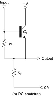
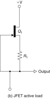
Several circuit modules have found their way into amplifier circuit design, and some of the more common of these are shown in Figure 9.26. Both the DC bootstrap, shown in Figure 9.26(a), and the JFET active load, shown in Figure 9.26(b), act to increase the dynamic impedance of R1, although the DC bootstrap, which can, of course, be constructed using complementary devices, has the advantage of offering a low output impedance. The amplified diode, shown as Figure 9.26(c), is a device that is much used as a means of generating the forward bias required for the transistors used in a push–pull pair of output emitter followers, particularly if it is arranged so that Q1 can sense the junction temperature of the output transistors. It can also be used, over a range of relatively low voltages, as an adjustable voltage source to complement the fixed voltage references provided by zener and avalanche diodes, band-gap references (IC stabilizers designed to provide extremely stable low voltage sources), and the wide range of voltage stabilizer ICs. Finally, when some form of impedance transformation is required, without the Vbe offset of an emitter follower, this can be contrived as shown by putting two complementary emitter followers in series. This layout will also provide a measure of temperature compensation.
Figure 9.26. Circuit oddments.


9.13. Slew Rate Limiting
This is a potential problem that can occur in any voltage amplifier or other signal handling stage in which an element of load capacitance (which could simply be circuit stray capacitance) is associated with a drive circuit whose output current has a finite limit. The effect of this is shown in Figure 9.27. If an input step waveform is applied to network (a), then the output signal will have a waveform of the kind shown at ‘a’, and the slope of the curve will reflect the potential difference that exists, at any given moment, between the input and the output. Any other signal that is present at the same time will pass through this network, from input to output, and only the high-frequency components will be attenuated.
Figure 9.27. Cause of slew rate limiting.

However, if the drive current is limited, the output waveform from circuit 9.27 (b) will be as shown at ‘b’ and the slope of the output ramp will be determined only by the current limit imposed by the source and the value of the load capacitance. This means that any other signal component that is present, at the time the circuit is driven into slew rate limiting, will be lost. This effect is noticeable, if it occurs, in any high-quality audio system and gives rise to a somewhat blurred sound—a defect that can be lessened or removed if the causes (such as too low a level of operating current for some amplifying stage) are remedied. It is prudent, therefore, for the amplifier designer to establish the possible voltage slew rates for the various stages in any new design and then to ensure that the amplifier does not receive any input signal that requires rates of change greater than the level that can be handled. A simple input integrating network of the kind shown in Figure 9.27(a) will often suffice.