1
Introduction to Carbon Structures
Meng‐Chih Su1 and Yuen Yung Hui2
1 Department of Chemistry, Sonoma State University, California, USA
2 Institute of Atomic and Molecular Sciences, Academia Sinica, Taipei, Taiwan
1.1 Carbon Age
Welcome to the Carbon World!
It seems that we already know the chemistry of carbon quite well, mostly in the form of graphite, through its long association with humans in history. Carbon is a simple element, predominantly (99% natural abundance of C‐12) containing the same number (6) of protons and neutrons, and therefore is radioactively stable. Of its other isotopes, C‐13 (1%) and C‐14 (<100 ppm), only C‐14 is radioactive with half‐life time lasting for a long 5730 year. It has been used routinely for the chronological tracking in archeology. With its relatively low mass, carbon is in the sixth place of all the hundred plus elements known today with an atomic number of Z = 6.
In nature, carbon ranks as the fourth element of cosmic abundance, after hydrogen, helium, and oxygen, and counts for about 20% by weight of all livestock and humans on earth, next only to oxygen (60%). Grouped together with silicon and germanium (4A group) in the Periodic Table of Elements, the chemical reactivity of elemental carbon may be considered inert compared to the neighboring nitrogen (5A) and oxygen (6A) groups because of its thermodynamic stability. Hence, graphite solid is used as a reference state for just about all thermodynamic measurements and data. Of course, such “inertness” is changed completely when carbon is combined with hydrogen, oxygen, and/or nitrogen − a whole world of interesting reactions will occur, and as we have learned in our college organic chemistry courses, the strong carbon chain becomes backbone of all organic molecules.
So, why carbon now? In science, carbon appears as one of the most common elements supporting of and interacting with a vast variety of materials since probably dawn of human civilization and, like a dear old friend, we thought we had known all there was to know about carbon. What is it so special about carbon, among all elements on our planet Earth, that scientists and researchers are now calling it the “carbon age” [1–3]? Specifically, why the carbon nanomaterials? Perhaps there is something about this old friend that we never knew, which can only be revealed as we look carefully into the nanometer regime of carbon. In this section, we trace the development of carbon nanomaterials in order to explore their molecular structures and intrinsic properties, which have shown great potential to many innovate practices and applications both in research and as commercial products.
1.2 Classification
Carbon nanomaterials have four major allotropes for biomedical applications: carbon nanotube (CNT), graphene (GR), nanodiamond (ND), and fullerene; all consisting of only carbon atoms, of which each has its own unique three‐dimensional nanostructure. These forms of carbon are often referred to as one‐dimensional CNT, two‐dimensional GR, three‐dimensional ND, and zero‐dimensional fullerene, based mainly on its structure and electronic properties.
Graphite is normally viewed as graphene layers stacking up in three dimensions and hence not an allotrope of its own. Multiple forms of carbon, including fullerene, CNT, GR, and ND, present a rich class of solid‐state materials that are both environmentally friendly and sustainable among other unique features each of their own.
1.3 Fullerene
A brief look in the history and development of carbon nanomaterials here seems in order to reacquaint us with some milestones in the development of new forms of carbon, with an emphasis on their unique structures and general features. A good place to start is when carbon nanoparticles first entered the center stage of science, as Richard Smalley, with help from Robert Curl, boldly introduced the world in 1985 with his soccer ball structure for the C60 molecule, now recognized as buckminsterfullerene (or fullerene, in short). An immense (and somewhat unexpected) passion caught up almost immediately in the science community to search for members of the fullerene family, to learn their chemistry, as well as to explore the possible applications of these new buckyballs. Indeed, C70, C76, C84, and other fullerene siblings were found in no time, all sharing a set of unique features as outlined here.
Fullerene is formed in a hollow cage made out of only carbon atoms with each carbon connected to three immediate neighbors in a small ring configuration, which consists of either five or six members, pentagonal, and hexagonal, respectively. As D'Arcy Thompson pointed out at the turn of the 1900s, no system of hexagons alone can enclose a space; it would need exactly 12 pentagonal rings in combination with a varying number of hexagonal rings to piece together a fullerene cage. This is known as Euler's theorem in geometry and topology, which states that the number of vertexes (V), edges (E), and faces (F) of a simple polyhedron is related by the formula V − E + F = 2.
For C60, as shown in Figure 1.1 [4], the 60 carbon atoms give V = 60; three bonds per atom and a total of 3 × 60 = 180 bonds, or 180/2 = 90 edges (each edge shared by two atoms). Following Euler's formula, 60 − 90 + F = 2, C60 has 32 faces (32 rings), i.e. 20 hexagonals and 12 pentagonals. Therefore, fullerenes are defined as “polyhedral closed cages made up entirely of n three‐coordinate carbon atoms and having 12 pentagonal and (n/2 − 10) hexagonal faces, where n is greater than or equal to 20.” So, C70 has 25 hexagonals, C84 has 32, and so forth. Other polyhedral closed cages made up entirely of n three‐coordinate carbon atoms are known as quasi‐fullerenes. Also shown in Figure 1.1 is that no two pentagonals can share the same edge, consequently, every carbon atom must belong simultaneously to one pentagonal and two hexagonal rings. Therefore, while C60 is shaped as a true buckyball (spheroidal), other fullerenes such as C70 appear as an oblong figure more resembling a rugby ball rather than a soccer ball.

Figure 1.1 C60 fullerene (or soccer ball) [4].
Fullerenes are stable molecules. C60, for example, weighs only 720 amu in a tiny size of about 1 nm in diameter, likely to survive even in galaxy and interstellar journeys. This had motivated Smalley (based on Harold Kroto's suggestions) to do experiments in searching for new and stable carbon species that may be present in outer space. In an early study of the chemistry of fullerenes [5], both C60 and C70 were discovered become superconducting when doped with alkali metals yielding a record high temperature at the time: 18° in Kelvin. On the other hand, when placed under favorable conditions (mostly photolytic catalyzed reactions), fullerene may become reactive with incoming nucleophiles, converting carbon's sp2 ‐hybridization to sp3 through nucleophilic additions. During the reaction, the hexagonal benzene rings remain largely inert as nucleophiles interacting with the electrons on the pentagonals. The change in hybridization, accompanied by a conformational change from the curved planar to a three‐dimensional structure, is believed to relax the overall surface strain, providing necessary stability for the final product.
In 1996, the Nobel Prize in chemistry was awarded to Robert F. Curl Jr., Harold W. Kroto, and Richard E. Smalley “for their discovery of fullerenes.” It is clear now as we look back that the impact brought by the discovery of C60 is not merely the discovery of a new form of carbon in material; rather, it has opened our eyes to see the infinitive possibilities of new structures that can be constructed by familiar elements, carbon and beyond, and the applications never imaginable that they can bring to humans. After all, we may not know carbon, a dear old friend of ours, as well as we have thought we did.
1.4 Carbon Nanotubes
Around 1990, while exploring new forms of fullerenes, Smalley suggested the possibility of tubular fullerene: a straight segment of carbon tube capped, perhaps, by two hemispheres of C60 on both ends of the tube. While Smalley's idea may or may not link directly to the grand entry of CNTs to the scientific world, certainly when Sumio Iijima of NEC (Japan) reported the first observation of multiwall nanotubes (MWNT) [6] in the following year (1991), the world was brought to witness yet another wave of awes and wonders of another new form of carbon. Iijima was able to demonstrate clearly the presence of concentric nanotubes produced by arc discharge evaporation of graphite, each comprised of 2–50 layers of carbon sheets. At the center, the smallest hollow tube has a diameter of 2.2 nm with additional layers each separated from the adjacent others by 0.34 nm, matching the distance between two adjacent layers in bulk graphite. Two years later, in 1993, single‐walled carbon nanotube (SWNT) was identified for the first time in a lab by Iijima and Ichihashi [7] and, independently, by Bethune et al. [8]. SWNT is recognized as rolling a single layer one atom thick of sp2 ‐hybridized carbon sheet into a cylindrical configuration with the diameter ranging from few angstroms to nanometers, all depending on the particular method and conditions of synthesis. The length typically varies from hundreds of nanometers to micrometers [9].
The strong carbon–carbon bonds and the network they have formed make CNTs 375 times stronger than steel and only 1/16 as dense. As a result, CNTs have found their commercial use easily in lightweight applications, such as bicycle frames and golf clubs. With its enormous specific surface area, >1600 m2 g−1 , SWNT shows an extraordinary surface adsorption capability comparable or, in some cases, better than activated carbon as an adsorptive material, all because of its highly unusual structure.
1.4.1 Structure
Almost all of CNT's intrinsic properties are derived from its 3‐D structure, which at first glance looks like “chicken wire,” all composed of six‐member rings. We use SWNT here as an example to describe parameters necessary to define the CNT structure. As shown in Figure 1.2 [10], a single‐layer nanotube can be pictured as cutting off a section from carbon sheet, represented by dashed lines on the figure, and rolling it over to seal on both edges (dashed lines) seamlessly so that at any point along one edge (for example, point A) will match an equivalent point A' on the other edge perfectly, and a cylindrical tube is thus formed. Depending on how the section is cut, the relative orientation of the cuts with respective to the sheet will determine the structure of CNT and, more than anything else, many of its physical properties. Furthermore, the orientation of these cuts and the size of the tube (in diameter) are all defined by a pair of numbers, called the chiral index (n, m), which is described below.
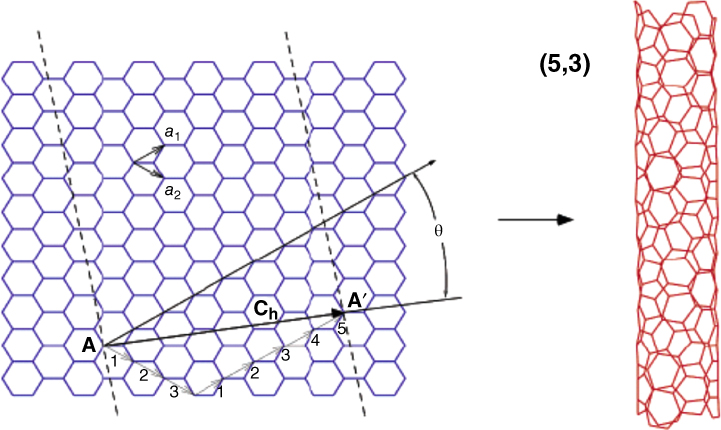
Figure 1.2 SWNT formed from carbon sheet to show unit vectors, chiral vector, chiral index, and angle [10].
The first and foremost structural parameter to describe nanotubes is the chiral vector, C h (Figure 1.2), which follows along the circumference of the tube and is perpendicular to the wall. C h connects two equivalent sites (A and A′) on a graphene sheet and is defined as C h = n a1 + m a2 , where a1 and a2 are unit vectors of the hexagonal honeycomb lattice and n and m are integers. Chiral vector C h also defines a chiral angle, θ, which is the angle between C h and the zigzag direction of the graphene sheet (Figure 1.2). In a sense, the zigzag vector originated at point A, which intersects only joining points of rings, defines the orientation of the carbon sheet, whereas C h results from CNT. The angle θ is related to chiral index as θ = tan −1 [(3)1/2 m/(2n + m)]. In addition, the diameter (d) of the tube is based on chiral index, d = [((3)1/2 /π)(m 2 + mn + n 2 )1/2 ] d cc, where d cc is the C─C bond length (0.142 nm). Now it is clear that every nanotube topology can be characterized by the pair of (n, m), which in turn defines the unique symmetry of CNT as chiral or achiral (armchair (n, n) or zigzag (n, 0)), see Figure 1.3 [11]. We will have a lot to say about chirality later because it is tied closely to the electronic properties of CNT. For now, the example in Figure 1.2 shows a chiral index of (5,3), which is a chiral SWNT, with a chiral angle of θ = 22° and diameter d = 0.55 nm.
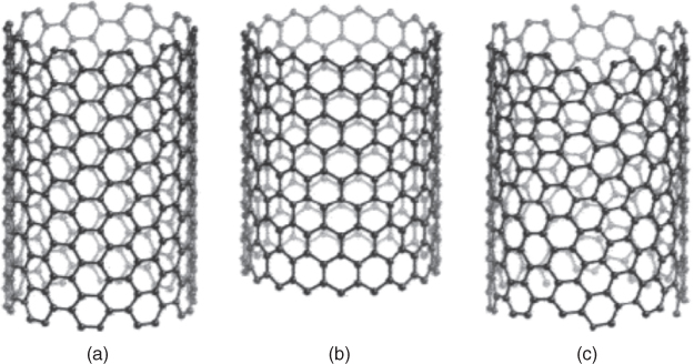
Figure 1.3 Schematic diagram of three representative SWNT structures in similar diameter: (a) armchair; (b) zigzag; and (c) chiral [11].
1.4.2 Electronics
A promising direction for the future of electronics is aligned with molecular electronics [12], in which the active part of the device is composed of a single or a few molecules, and the most actively studied forms of molecular electronics are based on CNT. Depending on their chirality and diameter, CNTs can be metals or semiconductors. The huge aspect ratio (tube length/diameter) of CNT makes it an ideal one‐dimensional (1D) electronic system, drastically reducing charge carrier scattering. It was found that 1D carbon crystalline lattice could conduct electricity at room temperature with virtually no resistance, a phenomenon known as ballistic transport, where electrons can move freely through the structure without any scattering from atoms. Furthermore, the lack of interface states as in the silicon/silicon dioxide interface provides greater flexibility to the fabrication process. All these fascinating properties (and more) came from CNT's unique electronic structure, as briefly described below.
CNT can be considered as rolling a section from a carbon sheet, and as such, the electronic structure of CNT is also derived from graphene, whose electronic properties will be discussed latter and should be cross‐referenced if necessary. Instead of going over rigors of band theory, which is a fascinating subject of its own, we use examples here through developing CNT's energy band structure. In Figure 1.4a, a SWNT is folded in the (5, 2) chirality, i.e. C h = 5a 1 + 2a 2, which has a 0.49 nm tube diameter [13]. Let's now look into the band energies starting with graphene. Quantum mechanical computation has calculated the band energy of graphene, and a three‐dimensional representation of the valence and conduction bands is shown as π‐ and π*‐bands, respectively, in Figure 1.4b. Graphene is a semimetal with two energy bands degenerate only at six corners of the hexagonal first Brillouin zone in K‐space. This can be seen in the top diagram of Figure 1.4b, where the two energy surfaces of π‐ and π*‐bands touch each other at six quantum states (or, 6 K‐points of the first Brillouin zone), which leaves no energy gap between the two bands; electrons are free to conduct and, hence, graphene is metallic. The energy of these 6 K‐points are at the Fermi level, so they are referred to as the Fermi points located on the Fermi surface.
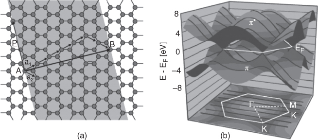
Figure 1.4 Construction of CNT (5, 2) and band structure of CNT (3, 3) [13].
Now we apply boundary conditions unique to SWNT and consider the transitions allowed between the valence and conduction bands. It is clear that the wavefunction describing electron behaviors on the nanotube must be forming a standing wave along the circumference of the tube, i.e. kC h = 2πq, where k is the wave vector aligned with the tube circumference (and C h) and q is an integer, so that k is quantized. Consequently, only a subset of graphene's states is allowed when it is rolled into a SWNT. For example, in the bottom diagram of Figure 1.4b, the dark lines represent the allowed states of a (3, 3) nanotube that transitions are allowed between bands. If the states pass through a K‐point (as in this case), the tube is metal and shows electrical conductivity, but if not, the tube is a semiconductor with a band energy gap. Whether a SWNT is a metal or semiconductor depends on its chiral index: If (n − m)/3 = 0 or integer, it is metallic; if not, semiconducting, which means, statistically, only one‐third of CNTs would show a metallic nature. Following this simple rule, both of our examples in Figure 1.4, chiral indices of (5, 2) and (3, 3) are metallic CNTs, whereas in the previous example shown in Figure 1.2, (5, 3), the SWNT is a semiconducting CNT.
With a basic understanding of how band energy is constructed for CNTs, we can zoom in those states responsible for electron transitions, which in turn will determine electronic properties unique only to CNTs. The density of states (DOS) is defined as the number of allowed electron states at a particular energy. Figure 1.5 includes a generalized representation of DOS in various dimensions for carbon nanomaterials [15]. The zero‐dimensional (0D) fullerene has DOS that is discrete in well‐defined energy levels. One‐dimensional (1D) CNTs split each band in sharp peaks DOS, van Hove singularities, which resemble molecular energy levels. In a simple term, for example, the allowed electronic transitions for SWNTs take place between matching peaks shown in the 1‐D DOS. These transitions are labeled as Ejj (E 11, E 22, etc.). The transitional energy varies inversely with nanotube diameter (d) according to
where a C‐C is the C─C bond length (0.142 nm) and γ 0 is the adjacent C─C interaction energy [14]. Therefore, a large size CNT is expected to have relatively small transitional energies.

Figure 1.5 Schematic diagram of energy vs. density of states (DOS) for carbon nanomaterials of various dimensions. Occupied electron energy levels (valence band) are shaded and unoccupied levels (conduction band) are white. The first two allowed absorption transitions (E11 and E22) are labeled for the 0D and 1D [14].
In summary, the unique electrical properties of CNTs arise from the confinement of the electrons in a tiny tubular structural configuration, which allows motion in only two directions along the tube axis: forward and backward. With the requirements that energy and momentum must be conserved, these constraints lead to a reduced phase space for the scattering processes that are responsible for the electrical resistance of all CNTs. Because of the reduced scattering, CNTs can carry enormous current densities, as reported, up to 109 A cm−2 without being destroyed [15]. This density is about two to three orders of magnitude higher than Al or Cu. Indeed, CNT is a promising star rising to future electronics. In the following 10 years since the first discovery of CNT, there were nearly 18 000 published CNT papers, setting a phenomenal record for a single material in the public interests.
1.5 Graphene
For all we know, graphene may have been around us for ages. Nevertheless, it was only in 2004 that Konstantin Novoselov and Andre Geim elegantly (using Scotch tape) isolated single‐ and few‐layer of “suspended” graphene from highly oriented pyrolytic graphite [16]. Graphene is characterized as individual or few‐layer stacked sheets of sp2 ‐ hybridized carbon where the number of sheets does not exceed 10 [17]. The structure of graphene is referred to as infinite polycyclic aromatic hydrocarbons (PAH) containing an infinite number of benzene rings fused together. Graphene is the first two‐dimensional nanomaterial known to exist in a suspended form, defying previous conventional knowledge that two‐dimensional material would have been too thermodynamically unstable to exist. In fact, with intrinsic strength of 130 GPa, Young's modulus per layer of 350 N m−1 , and breaking strength of 42 N m−1 , graphene is one of the world's strongest material ever discovered and thus warrants a title as a super carbon [18].
As a 2D crystalline membrane, graphene possesses a set of unique properties, collectively, surpassing any other material known today. These properties include an exceedingly large specific surface area (2630 m2 g−1 ), low density (<1 g cm−3 ), ultrahigh charge mobility (>2 × 105 cm2 V−1 s−1 ), excellent electrical conductivity (106 S cm−1 ) and thermal conductivity (>5000 W m−1 K−1 ), a uniform broadband optical absorption ranging from ultraviolet UV to far infrared (IR), and superb mechanical strength and unusual flexibility (as mentioned above). To provide a general understanding and appreciation for these extraordinary physical properties, we take a structure–property approach in explaining the cause‐and‐consequence relation of graphene, starting with simple valence bond theory.
1.5.1 Structure
The honeycomb structure of graphene is constructed by PAH of benzene rings (see above) where each carbon atom uses three of its four valence electrons to form sp2 ‐hybridized covalent bonds with three co‐planar neighboring carbons. The fourth valence electron occupies the carbon's pz orbital that forms π‐bonds shared equally in three directions leading to a C─C bond order of 1 and 1/3. Delocalized π‐electrons now spread over on a continuous layer of honeycomb consisting of short and rigid covalent bonds; together, the pool of π‐electrons provides graphene with an extremely strong stability capable of withstanding a great deal of mechanical strain and stress, indicated by its unusually high Young's modulus value (the ratio of normal stress over normal strain), making it one of the strongest material known. On a smooth flat surface like this, any injected charge carriers can run freely at an incredibly high speed, while the graphene sheet experiencing rapid lattice vibrations, i.e. phonons. Both effects contribute to excellent electrical and thermal conductivity. Furthermore, because all carbon atoms are identical and symmetrically arranged on the honeycomb plane, graphene is nonpolar and hydrophobic except at the edges; therefore, it has very poor solubility in water and/or common polar solvents used in lab, which actually imposes challenges on processing graphene functionalization.
1.5.2 Electronics
We now turn to electronic properties of graphene, the long‐continuing interest in physics since its debut in 2004, and the promising potential of graphene to be the building blocks for the next generation of electronics. It all starts with graphene's perfect conjugated structure. Following the tight‐binding model, in general, the valence electrons are assumed to occupy molecular orbitals delocalized throughout the entire solid molecule. Therefore, each carbon contributes one electron to the overall pool of π‐electrons on a graphene sheet. Meanwhile, the atomic orbital originally occupied by the valence electron of the carbon atom will now overlap with nearest neighbors to form a total of 2 N molecular orbitals for N carbon atoms of a graphene sheet. The energy levels of these molecular orbitals are close to each other and all together grouped in an energy band. Each band consists of (in order of increasing energy) bonding, nonbonding, and anti‐bonding states. At absolute zero in temperature, only the lower half of the graphene energy levels (or N molecular orbitals) are occupied and the energy level of the highest occupied molecular orbital (HOMO) is the Fermi level. Graphene has N π‐electrons that can fill all the way up to the Fermi level, and because there are empty orbitals very close to this level, it would take hardly any energy to excite the uppermost electrons. At temperatures above absolute zero, thermal motions of graphene can readily promote electrons to the unoccupied levels. Therefore, electrons can move extremely fast (and, hence, high charge carrier mobility), showing superb electrical and thermal conductivities.
Much interest has been focused on the behaviors of electrons around the Fermi level for the purposes of designing new electronic devices. The electronic structure of graphene was found to have a tiny overlap of its conduction and valence of π‐bands at Dirac point, according to Giem and Novoselov [19], which on the energy scheme is at the Fermi level. Therefore, graphene has zero band gap and behaves as a semiconductor. Some of its intriguing electronic properties derived from zero band gap, including features like massless Dirac fermions and anomalous quantum Hall effect, all require insight and understanding of the electronic structure of graphene that is beyond the scope of this book. Fortunately, because of intense interest and development in this area, the subject has been reviewed periodically and some are written at a level suited for beginners [20].
Now graphene is in the early stages of macroscale manufacturing for commercial use. As of January 2017, Project of Nanotechnology had surveyed 40 commercial products for CNT and graphene. There are examples of prototypes available as commercial products: conductive reinforcement coating on Kevlar fibers, fabrication of large‐area transparent electrodes, and high permittivity composites, only to name a few. Used in energy storage devices, the high surface area of graphene supports energy capacity that is cost‐effective far beyond any other material, i.e. in terms of energy per weight and cost. With all its intrinsic electronic properties, graphene is the top candidate to replace silicon‐based electronics, which is approaching its own material limit. Carbon‐based electronics when eventually commercially realized, promises to perform at lightning speed with superb capacity and, now more pressingly than ever, generate a green energy source that can benefit both socially and economically. Finally, as an endnote, Andre Geim and Konstantin Novoselov received the Nobel Prize in physics in 2010 “for groundbreaking experiments regarding the two‐dimensional material graphene.”
1.6 Nanodiamonds and Carbon Dots
Diamond is probably the best‐known allotrope of carbon, rooted in the history of the jewelry industry. In diamond crystal, every carbon atom is bonded to four other carbon atoms by sp3 hybridized orbitals. Diamond is a wide bandgap material with the highest hardness and thermal conductivity among natural bulk materials. Nanodiamond has similar physical properties, and has emerged as a promising candidate for biomedical applications owing to its high biocompatibility and low cytotoxicity [21]. In addition, its surface can be facilely functionalized for drug and gene delivery. Recently, the negatively charged nitrogen‐vacancy center in nanodiamond is of particular interest because its emission is in the optical region convenient for bioimaging as shown in Figure 1.6 [22]. The center absorbs strongly at 560 nm and emits fluorescence efficiently at ∼700 nm, well separated from cell autofluorescence. Furthermore, it is perfectly photostable without any sign of photobleaching even under high‐power excitation at the single molecule level. We will discuss more fully the bioimaging application of nanodiamonds in Chapter 4.
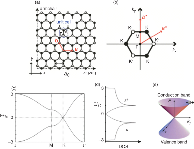
Figure 1.6 (a) Graphene honeycomb bipartite lattice structure in real space, where the black and white circles denote A‐ and B‐sublattice sites, respectively, a0 is the lattice constant and a = (a, 0) and b = (a/2, 3a/2) are the primitive vectors. The unit cell is indicated by a dotted hexagon. (b) First BZ of graphene. Reciprocal lattice vectors are denoted by a* and b*. K = 2π/a(1/3, 1/√3), K0 = 2π/a(2/3, 0), Γ = (0, 0). (c) π‐band structure of graphene along Γ‐M‐K‐Γ within the irreducible BZ. γ0 is the transfer integral between nearest‐neighbor carbon sites (γ0 = 3.16 eV). (d) Density of states (DOS) of the π band. (e) Three dimensional π‐band structure of graphene near the K point. Pseudospin is indicated by an arrow [20].
Finally, carbon dots are also known as carbon nanodots and carbon quantum dots. A carbon dot is a quasi‐spherical carbon nanoparticle with high oxygen content. Carbon dots have already inspired extensive studies for a wide range of applications [23], which will be the subject of Chapter 9.
Hope you enjoy the journey to the world of carbon nanomaterials!
Acknowledgment
This chapter, which sets the scene for the book, is an adaptation of the author’s own chapter Introduction to Nanotechnology from the forthcoming publication Fluorescent Nanodiamonds, First Edition, Huan‐Cheng Chang, Wesley W.‐W. Hsiao and Meng‐Chih Su. © 2018 John Wiley & Sons Ltd. Published 2018 by John Wiley & Sons Ltd.
References
- 1 Wang, Y., Wang, X.C., and Antonietti, M. (2012). Polymeric graphitic carbon nitride as a heterogeneous organocatalyst: from photochemistry to multipurpose catalysis to sustainable chemistry. Angew. Chem. Int. Ed. 51: 68–89.
- 2 Anastas, P.T. and Kirchhoff, M.M. (2002). Origins, current status, and future challenges of green chemistry. Acc. Chem. Res. 35: 686–694.
- 3 Corma, A. and Garcia, H. (2003). Lewis acids: from conventional homogeneous to green homogeneous and heterogeneous catalysis. Chem. Rev. 103: 4307–4365.
- 4 Diederich, F. and Whetten, R.L. (1992). Beyond C60: the higher fullerenes. Acc. Chem. Res. 25: 119–126.
- 5 Hebard, A.F., Rosseinsky, M.J., Haddon, R.C. et al. (1991). Superconductivity of 18K in potassium‐doped C60. Nature 350: 600.
- 6 Iijima, S. (1991). Helical microtubes of graphitic carbon. Nature 354: 56–58.
- 7 Iijima, S. and Ichihashi, T. (1993). Single shell nanotubes of 1‐nm diameter. Nature 363: 603–605.
- 8 Bethune, D.S., Kiang, C.H., Devries, M.S. et al. (1993). Cobalt‐catalyzed growth of carbon nanotubes with single‐atomic‐layerwalls. Nature 363: 605–607.
- 9 Georgakilas, V., Perman, J.A., Tucek, J. et al. (2015). Broad family of carbon nanoallotropes: classification, chemistry, and applications of fullerenes, carbon dots, nanotubes, graphene, nanodiamonds, and combined superstructures. Chem. Rev. 15: 4774–4822.
- 10 Charlier, J.‐C. (2002). Defects in carbon nanotubes. Acc. Chem. Res. 35: 1063–1069.
- 11 Sloan, J., Kirkland, A.I., Hutchison, J.L. et al. (2002). Structural characterization of atomically regulated nanocrystals formed within single‐walled carbon nanotubes using electron microscopy. Acc. Chem. Res 35: 1054–1062.
- 12 Joachim, C., Gimzewski, J.K., and Aviram, A. (2000). Electronics using hybrid‐molecular and mono‐molecular devices. Science 408: 541–548.
- 13 Avouris, P. (2002). Molecular electronics with carbon nanotubes. Acc. Chem. Res. 35: 1026–1034.
- 14 Carlson, L.J. and Krauss, T.D. (2008). Photophysics of individual single‐walled carbon nanotubes. Acc. Chem. Res. 41: 235–243.
- 15 Frank, S., Poncharal, P., Wang, Z.L. et al. (1998). Carbon nanotube quantum resistors. Science 280: 1744–1746.
- 16 Novoselov, K.S., Geim, A.K., Morozov, S.V. et al. (2004). Electric field effect in atomically thin carbon films. Science 306: 666–669.
- 17 Sun, Z., Kohama, S.‐I., Zhang, Z. et al. (2010). Soluble graphene through edge‐selected functionalization. Nano Res. 3: 117–125.
- 18 Savage, N. (2012). Super carbon. Nature 483: 530–531.
- 19 Geim, A.K. and Novoselov, K.S. (2007). The rise of graphene. Nat. Mat. 6: 183–191.
- 20 Fujii, S. and Enkoi, T. (2013). Nanographene and graphene edges: electronic structure and nanofabrication. Acc. Chem. Res. 46: 202–2210.
- 21 Vaijayanthimala, V., Cheng, P.‐Y., Yeh, S.‐H. et al. (2012). The long‐term stability and biocompatibility of fluorescent nanodiamond as an in vivo contrast agent. Biomaterials 33: 7794–7802.
- 22 Hsiao, W.W.‐W., Hui, Y.Y., Tsai, P.‐C. et al. (2016). Fluorescent nanodiamond: a versatile tool for long‐term cell tracking, super‐resolution imaging, and nanoscale temperature sensing. Acc. Chem. Res. 49: 400–407.
- 23 Hola, K., Zhang, Y., Wang, Y. et al. (2014). Carbon dots—emerging light emitters for bioimaging, cancer therapy and optoelectronics. Nano Today 9 (5): 590–603.