
Chapter 11
Chemical Sensors Based on Semiconductor Electronic Devices
A potentiometric ion sensor cell develop a potential difference (voltage) that depends on the activity of the target ion. This voltage is applied to a semiconductor electronic device called field-effect transistor (FET) that is included in the measuring instrument. This FET imparts a very high input impedance that prevents current flow through the cell and allows the measurement to be performed under equilibrium conditions. The current flowing through the FET depends on the applied voltage and additional electronic circuitry allows the voltage to be measured.
A further step in the development of potentiometric sensors was achieved by integrating a ion-responsive membrane with a FET-type structure (P. Bergveld, 1970). In this way, the potential difference developed at the membrane-solution interface directly affects the electrical parameters of the device and the response signal is represented by an electrical parameter of the FET structure.
As in the case of standard potentiometric sensors, FET-based ion sensors can be utilized not only for ion determination but also as transducers in sensors based on recognition processes that give rise to ions, such as enzymatic reactions and gas dissolution that alter the ionic composition of the solution.
A standard FET includes a metal layer separated by a thin insulator film from the semiconductor component of the device. If the metal film is able to interact with a gas, the device functions as a gas sensor. The first gas sensor of this type was the hydrogen sensor introduced by I. Lundström et al. in 1975.
This chapter gives first a brief overview of semiconductor properties and introduces several electronic semiconductor devices commonly emplyed in the development of chemical sensors, such as FETs and metal-insulator-semiconductor capacitors. The next section addresses ion sensors based on field effect devices. This section also presents gas sensors and enzymatic sensor using semiconductor device ion sensors as transducers. The final section is devoted to gas sensors based on field effect semiconductor devices.
Doped silicon is the typical semiconductor material used in field effect device chemical sensors. As will be shown in this chapter, new semiconductor materials (such as certain nanomaterials and organic semiconductors) have been successfully applied to the development of chemical sensors.
11.1 Electronic Semiconductor Devices
Electronic semiconductor devices, such as diodes and transistors, are essential components of any kind of electronic equipment. Such a device allows the current flow in electrical circuits to be controlled in order to perform information conveying and processing [1].
The functioning of semiconductor devices depends in an essential way on the density of the electric charge at the semiconductor surface. The charge density can build up simply under the effect of applied electric field. However, the charge density can also be modulated upon chemical interaction of the device with ions or molecules. This is the basis for the application of semiconductor devices as chemical sensors [2–4].
11.1.1 Semiconductor Materials
Currently, the standard semiconductor material in electronic devices is silicon, a group IV element that has four valence electrons available for chemical bonding. In a pure silicon crystal each valence electron is paired with another electron in a covalent bond with an adjacent atom. Apparently, no free electrons exist in pure silicon and the material is expected to behave as an insulator. However, the thermal agitation can release sporadically free electrons into the crystal lattice leaving a partially filled valence orbital (Figure 11.1A). So, charge carriers appear in the form of free electrons and positive vacancies (holes). Free electrons can move in an ordered way under the action of an electrical field as they do in a metal. At the same time, a bound electron can jump to a hole at an adjacent atom and this effect gives rise to a hole drift in a direction opposite to that of the free electrons. However, at normal temperatures, the free electrons and holes density are extremely low and pure silicon has therefore a very low conductivity. Such a material is an intrinsic semiconductor and is characterized by the occurrence of both free electrons and holes with equal concentrations.
Figure 11.1 Effect of silicon doping with group V or group III elements. Adapted from http://hyperphysics.phy-astr.gsu.edu/hbase/solids/dope.html#c2. Last accessed 17/05/2012.
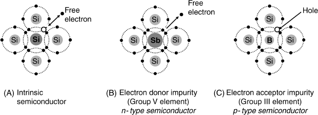
Enhanced silicon conductivity can be obtained by controlled addition of tiny amounts of impurities in a process termed semiconductor doping. Silicon doping can be performed by either group V or group III elements as shown in Figure 11.1. If a group V element serves as dopant (antimony in Figure 11.1B), its atoms enters the crystal lattice with five valence electrons. Four of these electrons form covalent bonds with silicon atoms, whereas the fifth one cannot find an available bonding orbital and remains in the unbound state. At the same time, the antimony atom becomes positively charged. As a result of the antimony doping, a large density of free electrons appears in the crystal lattice that leads to an enhanced conductivity. Such a doped crystal is termed an n-type semiconductor because the majority charge carriers are negatively charged electrons.
If the doping element belongs to the group III (boron in Figure 11.1C), its atom brings only three valence electrons. The boron atom forms four valence bonds with silicon atoms, but one of the bonding orbitals is partially filled with one electron contributed by a silicon atom. This orbital is actually a positive hole; its charge is balanced by the negative charge of the boron atom assumed after accepting an electron from an adjacent silicon atom. A silicon crystal doped with a group III element is termed a p-type semiconductor because the majority charge carriers are positively charged holes.
11.1.2 Band Theory of Semiconductors
The properties of semiconductors can be formulated more accurately in terms of the electronic band structure that accounts for the electrical resistivity of metal and semiconductors. An electronic band is formed of a large number of closely spaced molecular orbitals. Metals contain a band that is partly empty and partly filled regardless of temperature. Consequently, electrons can move freely in a lattice of positively charged atoms, which explains the high electrical conductivity of metals.
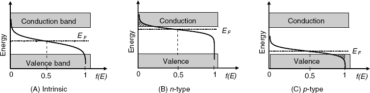
In semiconductors, one can distinguish a valence band and a conduction band. The valence band is the highest range of electron energies in which electrons are normally present at absolute zero temperature. Electrons with the energy in this rage are bound to individual atoms. The uppermost, almost unoccupied band is called the conduction band because only when electrons are excited to the conduction band can current flow in these materials. In semiconductors, the valence and conduction bands are separated by an energy bandgap (of about 1.1 eV for silicon) where no electron state exists (Figure 11.2A).
Figure 11.2 Band structure of semiconductors. The curve represents the Fermi–Dirac distribution.
The probability that a given available electron energy state E will be occupied at a given temperature is indicated by the Fermi–Dirac function f(E):
(11.1) ![]()
where kB is the Boltzmann constant and T is the absolute temperature. The constant EF represents the Fermi level that is the energy at which the probability of occupation by an electron is one-half. The Fermi–Dirac function demonstrates that at ordinary temperatures most of the allowed levels up to the Fermi level are filled, and relatively few electrons have energies above the Fermi level.
In an intrinsic semiconductor, the Fermi level lies close to midbandgap and, even if an electron is released from the valence band, it is not allowed to occupy the Fermi level. The single alternative for the electron is to be promoted to the conduction band by excitation. However, at normal temperatures this is a much less probable event because the bandgap is much larger than the average thermal energy. Consequently, at normal temperatures the electron population of the conduction band is extremely sparse; thereby the very low conductivity of intrinsic semiconductors. This intuitive conclusion is confirmed by the Fermi–Dirac function that predicts an extremely low probability that levels in the conduction band are occupied by electrons.
Doping of the semiconductor affects significantly the position of the Femi level due to the charges located at doping atoms. In n-semiconductors (Figure 11.2B) the Fermi level shifts close to the conduction band. In this situation, the Fermi distribution indicates a small but still significant probability that electrons occupy energy levels at the bottom of the conduction band (hatched area) and contribute to electrical conductivity.
In the case of a p-semiconductor (Figure 11.2C), the Fermi level is shifted near the conduction band. The Fermi–Dirac function indicates that the degree of occupation of energy states by electrons is smaller than unity at the top of the valence band (hachured area). The unoccupied states represent hole levels. Therefore, valence electrons can jump from a neutral atoms to an adjacent hole under the action of an electric field. This process is equivalent to hole drift in the opposite direction and accounts for hole conduction in p-semiconductors.
Therefore, by doping a pure silicon crystal one obtains either an n-semiconductor or a p-semiconductor, according to the number of valence electrons of the doping element. In the first case, the current flow through the material is due to the movement of free electrons in the conduction band, whereas in the second case the electric conduction is ensured by the holes drift in the valence band.
11.1.3 Metal-Insulator-Semiconductor (MIS) Capacitors
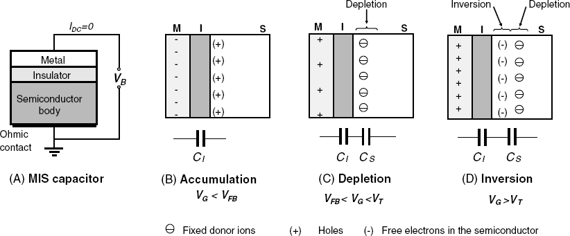
Certain electronic semiconductor devices are based on a sequence of well-matched layers of metal, insulator and semiconductor (MIS). The thickness of the metal and insulator layer is about 50–100 nm. Such a simple structure forms a MIS capacitor (Figure 11.3A), whilst more advanced devices, such as the MIS transistor include additional elements (Section 11.1.4).
In a MIS capacitor the semiconductor body is connected to the ground through an ohmic contact and a bias voltage (VB) is applied between the metal and the semiconductor (Figure 11.3A). As a result, the same amount of charge, but with opposite sign, appears in the metal film and at the upper limit of the semiconductor. As will be shown later, the particular feature of this capacitor is that its specific capacitance depends on the electric field created by the applied voltage. Hence, the MIS capacitor is a field effect device (FED), that is, a semiconductor device whose properties are determined largely by the effect of an electric field upon a certain region within the semiconductor.
Figure 11.3 (A) Cross section of a p-semiconductor based MIS capacitor; (B–D) operation regimes of a p-semiconductor MIS capacitor. M, I, and S stands for metal, insulator and semiconductor, respectively.
The capacitance can be measured by superimposing a small-amplitude AC voltage over the DC bias voltage. The AC current produced in this way is proportional to the capacitance.
There are three possible regimes of operation for a MIS capacitor, as shown in Figures 11.3B–D for the case of a p-semiconductor. In the accumulation regime (B), a negative bias is applied on the metal electrode. In response, positive holes accumulate at the semiconductor surface and the device behaves as a normal plate capacitor (CI) with the insulator as intermediate dielectric. Under these conditions, the device capacitance is at its maximum level (CI = Cmax, Figure 11.4A).
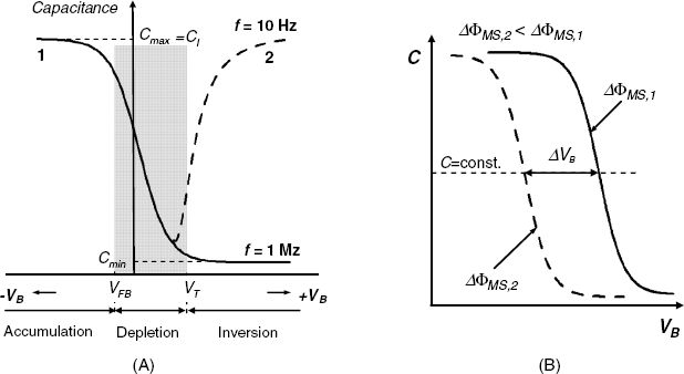
Figure 11.4 (A) Capacitance–voltage curves of a MIS capacitor as measured at high-frequency (curve1) and low-frequency (curve 2) applied AC voltage; (B) effect of the work-function difference at a high-frequency AC voltage.
The depletion regime occurs when a slight positive bias applied to the metal repels the holes away, leaving at the surface only the fixed doping atoms that bear negative charges. As a result, two different dielectric layers are present, namely the actual insulator and the depleted region. Under these conditions, the MIS capacitor behaves as two capacitors in series (CI and CS, Figure 11.3C) and the overall capacitance is:
(11.2) ![]()
Hence, in this case, the overall capacitance is smaller than CI.
On increasing the positive bias voltage, the thickness of the depletion layer increases and, consequently, the CS capacitance decreases while the surface is being depleted. Therefore, the total capacitance also decreases (Figure 11.4A, curve 1). The voltage at which the depletion layer sets on is termed flat-band voltage (VFB). This name derives from the fact that under flat-band conditions there is no excess charge in the semiconductor and the energy band is flat throughout the semiconductor up to the surface.
Over a particular positive bias voltage level called the threshold voltage (VT), free electrons, which are present as minority carriers, are driven to the silicon surface thus turning locally the p-semiconductor into an n-semiconductor (Figure 11.3D). Inversion of the carrier type gives rise in this way to an inversion layer. Its position in the depletion layer depends on the relation between the speed of the charge carrier generation/recombination and the frequency of the excitation AC voltage.
The measured capacitance of a MIS capacitor depends on both the bias voltage and the frequency of the applied AC voltage, as shown in Figure 11.4A.
The curve 1 in Figure 11.4A represents the capacitance measured at a high-frequency AC voltage (for example, 1 MHz). The effect of frequency is due to the fact that this parameter determines the position of the inversion layer. At very high frequencies the measured capacitance decreases within the depletion region (Figure 11.4A, curve 1). Within the inversion region, the inversion layer is formed at the inner limit of the depletion layer that is, in the semiconductor bulk. Hence, the capacitance attains a constant, minimal value Cmin. At low frequencies (for example, 10 Hz) the charge-carrier concentration can follow the variation in the AC voltage. Within the depletion region, the low-frequency capacitance varies according to curve 1. However, within the inversion region, the inversion layer is built up at the surface of the semiconductor. Therefore, within this region the capacitance increases with the voltage (Figure 11.4A, curve 2) and, in strong inversion, the capacitance recovers the maximal value.
The threshold voltage is the key parameters in the functioning of FED sensors. Its physical meaning can be derived by considering the charge balance under inversion conditions. To this end, the charge per unit area (surface charge density) for each charged layer in the system will be considered. It should be noted that due to the characteristics of the fabrication process, there are always fixed and mobile charged sites within the insulator layer and the overall charge in the insulator should also be taken into account. Therefore, the charge balance condition of the MIS structure under inversion conditions can be formulated as follows:
(11.3) ![]()
Notice that ![]() is the maximum achievable charge in the depletion layer. At the threshold voltage (
is the maximum achievable charge in the depletion layer. At the threshold voltage (![]() ), the inversion layer is not yet set in, so, the charge-balance equation in this particular case is:
), the inversion layer is not yet set in, so, the charge-balance equation in this particular case is:
Equation (11.4) represents the physical condition for the onset of the inversion regime. An analysis of the potential distribution across the MIS system demonstrates that the threshold voltage depends essentially on the work-function difference between the metal and the semiconductor.
The work function is the minimum energy needed to remove an electron from the Fermi level of a neutral metal or semiconductor to vacuum. The emitted electron should be located at a point immediately outside the solid surface such that the electron does not experience electrostatic effects induced by the solid. The energy level occupied by this electron is the first nonbounded state and is usually termed the vacuum level. According to this definition, the work function is determined by both the bulk properties of the solid and the state of its surface (which determines the vacuum level).
The functioning parameter that depends on the work function is the threshold voltage of the MIS device. More precisely, the threshold voltage depends on the work-function difference between the metal (![]() ) and the semiconductor (
) and the semiconductor (![]() ), as follows:
), as follows:
where ![]() , e is the elementary charge and
, e is the elementary charge and ![]() is a constant term.
is a constant term.
Equation (11.5) is the basis of the chemical sensing by means of MIS devices. MIS sensors are designed such as to undergo a variation in ![]() in response to the interaction with the analyte. Details of the analyte action on
in response to the interaction with the analyte. Details of the analyte action on ![]() are given in further sections dealing with specific MIS sensors. In the particular case of a MIS capacitor, a change in
are given in further sections dealing with specific MIS sensors. In the particular case of a MIS capacitor, a change in ![]() results in the current–voltage curve being shifted in accordance with Equation (11.5) as shown in Figure 11.4B. The sensor response in this case is the bias voltage difference at a constant capacitance (
results in the current–voltage curve being shifted in accordance with Equation (11.5) as shown in Figure 11.4B. The sensor response in this case is the bias voltage difference at a constant capacitance (![]() ).
).
Figure 11.4B displays schematically capacitance–voltage curves recorded at a high frequency (1 MHz). The bias voltage shift can also be inferred from low-frequency curves that are similar to curve 2 in Figure 11.4A. In this case, the voltage shift is indicated by the shift of the minimum point on the curve.
It should be kept in mind that modulation of the work function by the interaction of the analyte with the sensor is the key functioning principle of semiconductor-based chemical sensors. A detailed approach to this topic is available in refs. [5, 6].
11.1.4 Metal-Insulator-Semiconductor Field Effect Transistors (MISFETs)
MISFETs are electronic devices with tunable electric resistance. In order to understand the functioning of MISFETs it is useful to consider first at a simpler device, namely the p-n junction diode. As its name suggests, this device consists of two semiconductor zones of different type (Figure 11.5A). When a p-n junction is build up, some of the electrons from the n-region are free to diffuse across the junction and recombine with holes. Filling a hole makes a negative ion and leaves behind a positive ion on the n-side. Thus, the junction region turns depleted of charge carriers.
Figure 11.5 The semiconductor diode.
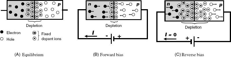
A current can cross the diode only if a voltage source is connected with the negative pole to the n-region and the positive pole to the p-region (forward bias, Figure 11.5B). In this case, the electrons from the n-type semiconductor are injected in the p-type one and also, holes from the p-type semiconductor are injected in the n-type one. Hence, the depletion region collapses, becoming thinner. In this state, the diode shows less resistance to current passing through it. In order for a sustained current to go through the diode, though, the forward voltage should be above a certain limit such that the depletion region becomes fully collapsed. In practice, the current has to be limited by a resistor, otherwise the diode will be thermally destroyed.
If the source polarity is reversed (reverse bias, Figure 11.5C) charge carriers in each zone are attracted to the periphery leaving a wide depletion zone in the junction region. Under these conditions, the diode displays a very large resistance and the current through the diode is insignificant. Diodes are used to convert alternating current to direct current, a process known as rectification.
A diode displays only two states, on or off, in accordance to the polarity of the applied voltage. In contrast, the transistor is a device that allows tuning the current between zero and a certain limit by proper adjustment of some electrical parameters. The structure of a field-effect transistor is shown schematically in Figure 11.6A. It consists of a small piece of p-type silicon (substrate) with two n-type regions formed at the upper left and right extremities. The two n-type regions are called source and drain, respectively. The surface is covered by an insulating layer (for example, SiO2) and a thin metal layer is deposited above it to form the gate. If a voltage VD is applied between the source and the drain, no current flow is possible because reverse biasing occurs at one of the two p-n junctions no matter what the drain source polarity is. The situations change if a positive electric charge is loaded on the gate by means of the VG voltage source. By electrostatic interaction, this positive charge drives free electrons from the source to the substrate surface layer. In this way, the p-semiconductor turns into an n-type one within a very thin layer below the gate; hence the name inversion layer ascribed to this zone (see Section 11.1.3 for details). Now, there are no more p-n junctions, the source and the drain are shortcut and current flow is allowed. In other words, the electric resistance between the source and drain assumes a much lower value. Because the current flow is confined within the inversion layer, this zone is called a channel.
Figure 11.6 An n-channel enhancement mode MISFET. S: source; D: drain; G; gate.
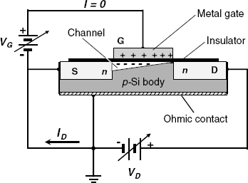
As the current flow is controlled by the electrical field produced by the gate, such a device is termed a field-effect transistor (FET). In accordance with the sequence of layers, this a device is also called a metal-oxide-semiconductor field-effect transistor, a MOSFET. As the insulator can be made of a nonoxide material (such as silicon nitride) such devices are more generally termed metal-insulator-semiconductor field-effect transistors (MISFETs).
It is important to note that the inversion layer forms only after the gate voltage overcomes the threshed voltage VT. If VG > VT, the volume density of electrons in the inversion layer is higher than the volume density of holes in the semiconductor body. The gate voltage therefore determines the electron density in the channel and hence, its electric resistance. The FET operation regime depends crucially on the quotient of ![]() and
and ![]() , If the
, If the ![]() condition is fulfilled, the drain current is given by the following equation in which
condition is fulfilled, the drain current is given by the following equation in which ![]() is a parameter depending on the physical and geometrical characteristics of the transistor:
is a parameter depending on the physical and geometrical characteristics of the transistor:
Hence, the current varies nonlinearly with the drain voltage, which is characteristic of the subthreshold region on the characteristic curve (Figure 11.7A). At very small drain voltages, the ![]() relationship is linear.
relationship is linear.
However, the source–drain potential difference produces a variation in the electron density along the channel. This is negligible at the onset of the subthreshold region, but increases considerably at ![]() . On increasing the drain voltage, a situation will arise when the free electrons are missing near the drain, which is connected to the positive pole of the drain source. In this case, the channel does not extend across the whole distance between the source and the drain. The onset of the depletion region is also known as pinch-off to indicate the lack of channel region near the drain. Nevertheless, the drain current can flow due to the high electron velocity caused by the source–drain potential difference. Any increase in the drain voltage speeds up the electrons, but, at the same time, increases the length of the depleted part of the channel and thereby moves the pinch-off point towards the source. As a result, the current displays only a slight increase with increasing drain voltage. This situation is characteristic of the saturation region in Figure 11.7A. In the saturation region, the drain current varies as:
. On increasing the drain voltage, a situation will arise when the free electrons are missing near the drain, which is connected to the positive pole of the drain source. In this case, the channel does not extend across the whole distance between the source and the drain. The onset of the depletion region is also known as pinch-off to indicate the lack of channel region near the drain. Nevertheless, the drain current can flow due to the high electron velocity caused by the source–drain potential difference. Any increase in the drain voltage speeds up the electrons, but, at the same time, increases the length of the depleted part of the channel and thereby moves the pinch-off point towards the source. As a result, the current displays only a slight increase with increasing drain voltage. This situation is characteristic of the saturation region in Figure 11.7A. In the saturation region, the drain current varies as:
As will be shown later, the dependence of the drain current on the gate voltage (Figure 11.7B) plays an essential role in chemical-sensor applications. In accordance with the previous considerations, the current is set up at VG = VT and increases as a parabola with increasing gate voltage within the subthreshold region according to Equation (11.6). In the saturation region, the drain current increases proportionally with (VG > VT)2, as shown in Equation (11.7).
Figure 11.7 Characteristic curves of a MOSFET. (A) Drain current vs. drain voltage at constant gate voltage. The broken line indicates the limit of the saturation region. (B) Drain current vs. gate voltage at constant drain voltage.
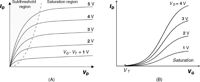
Figure 11.8 Symbols for enhancement mode MOSFET devices.
A suggestive analogy for the FET is the behavior of a water tap. The gate is analogous to the knob that controls the flow rate. If the knob is screwed up just a little, probably no water will flow at all. Further screwing up causes the flow to increase proportionally (subthreshold region). However, over a certain limit, the flow does not increase any longer (saturation). Under these circumstances, the flow can be increased only by increasing the water reservoir pressure (drain voltage).
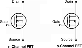
p-Channel transistors are also available; such a transistor is the mirror twin of the n-channel one. Hence, it is formed of an n-type semiconductor body and the gate is negatively polarized. Therefore, at a gate voltage over the threshold voltage, holes accumulate at the semiconductor surface to form the channel. Current flow through the channel is secured by hole drift under the action of the source–drain voltage.
The above types of transistor operate in the enhancement mode because the drain current is zero at zero gate bias, but increases with increasing gate voltage due to the increase in charge-carrier density within the channel. Common symbols for an enhancement-mode MOSFET are shown in Figure 11.8.
Another possibility is to form, by doping, a channel during the fabrication process. Hence, the drain current can flow at zero gate voltage. In order to control the drain current, the gate is biased so as to decrease the charge carrier density within the channel; hence a decrease in the drain current results. Such a device is a depletion mode transistor.
In summary, one can distinguish two operational regions of a MOSFET. For values of ![]() , the drain current is given by Equation (11.6). The device operates in the nonsaturated mode and behaves as a nonlinear, gate-voltage-controlled resistor. For values of
, the drain current is given by Equation (11.6). The device operates in the nonsaturated mode and behaves as a nonlinear, gate-voltage-controlled resistor. For values of ![]() , the drain current is given by Equation (11.7). In this case, the device operates in the saturation mode and the current is almost independent of the drain voltage.
, the drain current is given by Equation (11.7). In this case, the device operates in the saturation mode and the current is almost independent of the drain voltage.
The field-effect transistor is the key component in contemporary electronic equipment. It is available as an independent unit (in the mm size range), but, as a rule, a great number of submicrometer-size transistors are produced on a single silicon chip, along with other passive components to form integrated circuits. Transistor applications are based on the fact that the drain current can be modulated by means of the gate voltage at a constant drain voltage.
11.1.5 Outlook
Pure semiconductor materials (intrinsic semiconductors) have a very low electrical conductivity because most of the valence electrons are localized in the valence band, that is, are bound to the lattice atoms. The conductivity of a semiconductor material can be enhanced considerably by doping. If the doping element is an electron donor, one obtains an n-semiconductor in which the electric current is carried by free electrons. Doping by an electron acceptor element leads to p-semiconductors, which are characterized by hole conduction.
Field effect electronic devices are based on the control of charge distribution at the surface of a semiconductor bay means on an electric field. Typical devices of this type are the MIS capacitor and the MISFET. These devices are formed of a sequence of semiconductor-insulator-metal (gate) layers in which the metal gate is used to create the electric field that controls the device behavior.
A key parameter of FEDs is the threshold voltage, which is the gate voltage limit over which the inversion layer forms. The threshold voltage depends on the work-function difference between the semiconductor and the metal layer. As will be shown in next sections, the work potential difference plays an essential role in transduction by FEDs.
11.2 FED Ion Sensors and Their Applications
11.2.1 Electrolyte-Insulator-Semiconductor (EIS) Devices
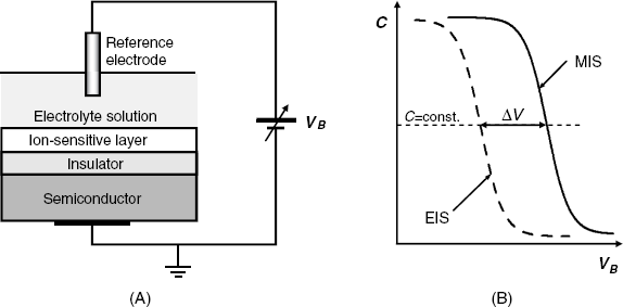
A field effect device can be converted into ion sensor if the metal gate is omitted, and, instead, an ion-responsive layer is build up over the insulator layer and put in contact with the test solution as shown in Figure 11.9A. The ion-responsive layers are generally similar to those developed in the field of potentiometric ion sensors. As the system includes an electrolyte solution, it is termed an electrolyte-insulator-semiconductor (EIS) that differs from the MIS system by the nature of the layer over the insulator. In order to control the charge distribution at the semiconductor surface, a bias voltage is applied through a reference electrode. In an EIS system, the metal in the reference electrode is an analogue of the metal gate in the corresponding MIS structure. By ion exchange with the solution, a characteristic potential develops at the interface between the solution and the ion-responsive layer. This potential alters a particular parameter of the device depending on the ion concentration in the solution. Comprehensive surveys of FED ion sensors are available in refs. [2, 4, 6–8].
Figure 11.9 (A) Schematics of an electrolyte-insulator-semiconductor ion sensor. The solution should be insulated from the solid device. (B) Capacitance–voltage curves for an MIS system and an EIS ion sensor.
In order to understand the transduction mechanism in an EIS device, the device will be represented as follows, for the case in which an Ag/AgCl reference electrode is used:
As shown in Scheme (11.8), a series of potential differences develops across this system, Thus, ![]() is the potential difference between the semiconductor and the insulator and is similar to that found in an MIS device.
is the potential difference between the semiconductor and the insulator and is similar to that found in an MIS device. ![]() is the potential difference between the insulator and the membrane and
is the potential difference between the insulator and the membrane and ![]() is the membrane potential that develops across the ion-sensitive layer. Finally, the potential difference between the reference electrode metal and the solution is written as
is the membrane potential that develops across the ion-sensitive layer. Finally, the potential difference between the reference electrode metal and the solution is written as ![]() .
.
In the case of a true MISFET, the threshold voltage is a constant parameter that is determined by the charge in the depletion layer, the work-function difference between the gate metal and the semiconductor and insulator charges. As shown before, the threshold voltage represents the particular value of the gate voltage needed for setting up the inversion layer. In the case of an EIS structure, additional potential difference terms come into play as shown in Scheme (11.8). Therefore, an electron that hypothetically passes from the semiconductor to vacuum has to cross several charged regions that affect its energy. The same happens with an electron transferred from the reference electrode metal to vacuum. Consequently, the threshold voltage equation (Equation (11.5)) should be altered in order to account for the additional potential terms in the EIS system, and the threshold voltage for the EIS system (![]() ) assumes the following form [2]:
) assumes the following form [2]:
Here ![]() represent the reference electrode potential plus the junction potential and can be assumed to be constant. If
represent the reference electrode potential plus the junction potential and can be assumed to be constant. If ![]() is held constant, the threshold voltage difference between the EIS and the MIS systems is represented by the membrane potential corrected by a constant term:
is held constant, the threshold voltage difference between the EIS and the MIS systems is represented by the membrane potential corrected by a constant term:
(11.10) ![]()
Hence, the capacitance–voltage curve of an EIS ion sensor shifts with the ion concentration in the solution as shown in Figure 11.9B. The change in the threshold voltage can be detected as the change in the bias voltage at a constant capacitance:
(11.11) ![]()
As the membrane potential is a logarithmic function of the ion concentration in the solution, a similar variation in the bias voltage will occur when varying the ion concentration.
By suitable modification of the device in Figure 11.9A, it can be turned into an ion-sensitive field-effect transistor (ISFET). In this case, the alteration of the threshold voltage produces a change in the drain current at a constant gate voltage. As will be shown in the next section, the response can be translated into a variation in the applied gate voltage at a constant drain current, which is formally similar to the capacitor response shown in Figure 11.9B.
Hence, the mechanism by which FED ion sensor devices respond to the analyte ion concentration is similar to that involved with potentiometric ion sensors. The response can be obtained as the variation in the gate voltage, which is analogous to the voltage response of a potentiometric sensor. Moreover, ion-recognition methods and materials developed in the framework of standard potentiometric sensors can be easily transposed to the design of FED ion sensors. That is why FED sensors are categorized as a particular kind of potentiometric sensor.
As shown before, FED ion sensors can in principle be designed in either the capacitor or the FET configuration. As it is simpler the capacitor design is preferable in the fabrication of ion sensor arrays [9, 10]. On the other hand, the capacitor version is more demanding as far as the measuring instrumentation and the data-processing procedures are concerned.
11.2.2 FED pH Sensors
The first application of field effect devices in ion chemical sensing was the FED-based pH sensor initially developed by Bergveld [11–14].
In a pH ISFET, the sensing element is the surface of the gate insulator (for example, silicon dioxide) that is put in direct contact with the solution. Under these conditions silanol sites (formulated as A-OH) develop at the oxide surface. The pH effect on such sites can be rationalized by the site-dissociation model, which assumes that the silanol site is able to undergo both acid dissociation and protonation as follows:
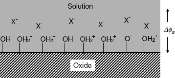
Here, ![]() represent the hydrogen ion concentration near the interface. As a result of the reaction of A – OH sites with the hydrogen ions, a double electric layer forms at the insulator/solution interface (Figure 11.10). It consists on the one side of the ionic sites at the oxide surface and, on the other side, of solution anions attracted by the positive charges at the surface. Consequently, a potential difference
represent the hydrogen ion concentration near the interface. As a result of the reaction of A – OH sites with the hydrogen ions, a double electric layer forms at the insulator/solution interface (Figure 11.10). It consists on the one side of the ionic sites at the oxide surface and, on the other side, of solution anions attracted by the positive charges at the surface. Consequently, a potential difference ![]() builds up at the interface of the oxide and the solution. This determines the surface concentration of the hydrogen ion at the surface as a function of the bulk concentration (
builds up at the interface of the oxide and the solution. This determines the surface concentration of the hydrogen ion at the surface as a function of the bulk concentration (![]() ) according to the Boltzmann equation:
) according to the Boltzmann equation:
(11.14) ![]()
where e is the elementary charge, ![]() is the Boltzmann constant, and T is the absolute temperature.
is the Boltzmann constant, and T is the absolute temperature.
Figure 11.10 Structure of the double electric layer at the oxide/solution interface. The double layer consists of fixed charges at the oxide surface and mobile anions (X−) driven from the solution by electrostatic attraction.
The A – OH site can behave as either an acid (reaction (11.12)) or base (reaction (11.13)), which implies an amphoteric character. Consequently, the assembly of ionogen sites forms a surface-confined pH buffer system. The buffer capacity of this system (![]() ) plays an essential role in determining the pH response. The buffer capacity measures the ability of the buffer to counteract a pH change when hydrogen ions are added or removed. This parameter depends on the above equilibrium constants and the total number of active sites per unit area (
) plays an essential role in determining the pH response. The buffer capacity measures the ability of the buffer to counteract a pH change when hydrogen ions are added or removed. This parameter depends on the above equilibrium constants and the total number of active sites per unit area (![]() ), as follows:
), as follows:
(11.15) ![]()
where k is a specific parameter of the insulator.
If ![]() , the following linear equation relates the surface potential to the solution pH:
, the following linear equation relates the surface potential to the solution pH:
Here, ![]() is the pH value at which
is the pH value at which ![]() ; it is determined by the equilibrium constants (
; it is determined by the equilibrium constants (![]() ). A crucial issue is that the response sensitivity is determined by
). A crucial issue is that the response sensitivity is determined by ![]() , and a Nernstian response is obtained only if
, and a Nernstian response is obtained only if ![]() , that is, if there is a high surface buffer capacity. This condition is fulfilled when the surface density of ionogen sites is very high. In addition, the insulator layer has to be stable in contact with the solution so as to prevent solution reaching the semiconductor surface. The most suitable insulator materials for use in pH detection are
, that is, if there is a high surface buffer capacity. This condition is fulfilled when the surface density of ionogen sites is very high. In addition, the insulator layer has to be stable in contact with the solution so as to prevent solution reaching the semiconductor surface. The most suitable insulator materials for use in pH detection are ![]() ,
, ![]() (which can be formed by pulsed laser deposition) and
(which can be formed by pulsed laser deposition) and ![]() (which can be formed by plasma-enhanced chemical vapor deposition). In contrast to oxide materials, the
(which can be formed by plasma-enhanced chemical vapor deposition). In contrast to oxide materials, the ![]() surface displays two kinds of active site, namely silanol and primary silamine (Si-NH2) sites. The characteristics of various materials used in pH-sensing layers are surveyed in ref. [15].
surface displays two kinds of active site, namely silanol and primary silamine (Si-NH2) sites. The characteristics of various materials used in pH-sensing layers are surveyed in ref. [15].
Therefore, an insulator layer that develops a high ionogen site density by conditioning in water forms the hydrogen-responsive element of this pH sensor. By ion exchange with the solution it gives rise to an interface potential that is a linear function of the solution pH.
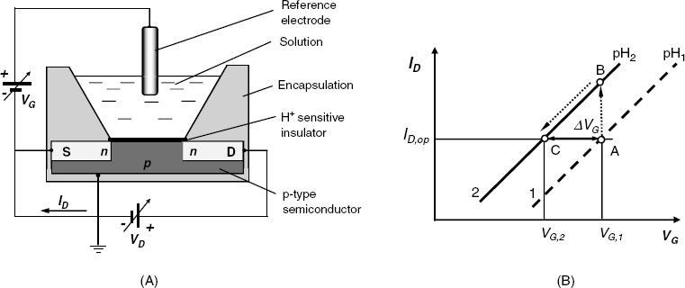
The layout of a pH FET sensor is shown in Figure 11.11A. In contrast to the standard FET, the metal gate is missing in this device. Instead, the H+-sensitive insulator layer is set in contact with the test solution and a gate voltage (VG) is applied via a reference electrode. The sequence of contacting phases can be formulated as follows:
The relevant potentials are also shown in Scheme (11.17). Here, ![]() is the reference electrode potential including the junction potential,
is the reference electrode potential including the junction potential, ![]() is the potential difference produced by the proton-transfer reactions (11.12) and (11.13),
is the potential difference produced by the proton-transfer reactions (11.12) and (11.13), ![]() is a constant potential difference due to the oriented solvent dipoles at the solution/insulator interface, and
is a constant potential difference due to the oriented solvent dipoles at the solution/insulator interface, and ![]() is a constant potential difference contributed by the solid-state part. Hence, the
is a constant potential difference contributed by the solid-state part. Hence, the ![]() ,
, ![]() and
and ![]() terms would alter the threshold voltage in the drain current equation of the FET device and the pertinent term in Equation (11.9) should be substituted so as to give Equation (11.18).
terms would alter the threshold voltage in the drain current equation of the FET device and the pertinent term in Equation (11.9) should be substituted so as to give Equation (11.18).
In this equation, each term except ![]() is pH independent and their sum will be further substituted by the constant k1. Under these circumstances, the drain current equation in the subthreshold regime assumes the following form:
is pH independent and their sum will be further substituted by the constant k1. Under these circumstances, the drain current equation in the subthreshold regime assumes the following form:
Taking into account Equation (11.16) it results that at constant gate voltage and drain voltage the drain current depends on the pH via the ![]() term.
term.
Figure 11.11 (A) The layout of a cell for pH determination by means of a pH ISFET; (B) the principle of constant drain current operation of an ISFET sensor.
The response in terms of voltage (potentiometric response) can be obtained under constant drain-current conditions. Thus, if an explicit relationship for the gate voltage is derived from Equation (11.19), one obtains upon assuming that ![]() the following expression:
the following expression:
Here, the constant term includes contributions from any pH-independent parameter as well as the constant drain current.
Therefore, the sensor response in terms of gate voltage at constant drain current is a Nernstian one with the ideal sensitivity determined by the prelogarithm factor (59 mV/pH unit at 25 °C). Actual sensors can display a slightly lower sensitivity. That is why both the constant term and the sensitivity in Equation (11.20) should be treated as empirical parameters and their values are obtained by calibration with standard pH buffer solutions, as in the case of the pH glass electrode.
The principles of constant drain-current operation can be made clear by means of the diagram in Figure 11.11B. Thus, according to Equation (11.19), at a given pH, the drain current is a function of the gate voltage. Assume that at pH1, the operating point is A with the coordinates ![]() , where
, where ![]() is the operational drain current. If the pH changes to pH2 at a constant gate voltage, the operating point shifts to B. However, if the gate voltage is lessened, the operating point moves downhill along the line 2. When the gate voltage value becomes
is the operational drain current. If the pH changes to pH2 at a constant gate voltage, the operating point shifts to B. However, if the gate voltage is lessened, the operating point moves downhill along the line 2. When the gate voltage value becomes ![]() , the
, the ![]() drain current will be restored to the initial value (point C). The
drain current will be restored to the initial value (point C). The ![]() value is related to pH2 by an equation derived from Equation (11.20).
value is related to pH2 by an equation derived from Equation (11.20).
The change in the gate voltage compensates for the variation in the interface potential in response to the pH modification. In practice, the gate-voltage adjustment is performed automatically by suitable electronics incorporated in the pH meter.
pH ISFET devices compare favorably with the pH glass electrode. Thus, the working range spans from pH 2 to 12 and the response time is less than 1 min. pH ISFET sensors with a remarkable ruggedness, stability, and accuracy are currently commercially available. In contrast to the pH glass electrode, a pH ISFET resists dry storage and does not need prolonged rehydration before use.
In an analogous way, capacitive pH sensors can be fabricated on the basis of electrolyte-insulator-semiconductor structures. In this case, the response is represented by the shift of the capacitance–voltage curve with the change in pH.
A great advantage of the pH ISFET sensor is the possibility of fabrication by microelectronics technology, which facilitates the mass production. Such a sensor is of about one millimeter size and is therefore suitable for integration in sensor microarrays along with additional electronics for parameter control and signal processing. Due to the simple structure of the device, the fabrication of capacitive sensor arrays is more facile.
The small size makes the pH FED sensor for in vivo applications [16, 17]. Thus, a catheter-type pH FED sensor of about 1 mm diameter has been developed [18].
11.2.3 pH ISFET-Based Gas Probes
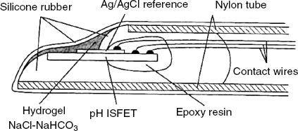
A Severinghaus-type CO2 sensor (analogous to that introduced in Section 10.16) can be obtained by using a pH ISFET sensor as transduction element. The small size of the FED sensor allows for miniaturization in view of in vivo applications, as shown in Figure 11.12. The included pH sensor has been fabricated on an elongated semiconductor substrate that has the sensitive region at one end and the bonding-pad region for lead wires at the opposite end. The sensing and bonding-pad regions have been isolated from each other by a ![]() double layer that extends also to front and back surfaces as well as to the gate wall. This provides good electrical insulation and makes the device waterproof. An Ag/AgCl reference electrode has been formed by vapor deposition of silver followed by chlorination. After covering the electrical bonding wires with epoxy resin, the chip is mounted in a nylon tube and fastened silicone rubber. The pH-sensitive gate region has been coated with a hydrogel. In this configuration, the device functions as a pH sensor. In order to convert it into a CO2 probe, a thicker gel impregnated with a NaCl-NaHCO3 solution was placed over the gate region and the whole assembly was coated with a gas-permeable silicone membrane by dip coating.
double layer that extends also to front and back surfaces as well as to the gate wall. This provides good electrical insulation and makes the device waterproof. An Ag/AgCl reference electrode has been formed by vapor deposition of silver followed by chlorination. After covering the electrical bonding wires with epoxy resin, the chip is mounted in a nylon tube and fastened silicone rubber. The pH-sensitive gate region has been coated with a hydrogel. In this configuration, the device functions as a pH sensor. In order to convert it into a CO2 probe, a thicker gel impregnated with a NaCl-NaHCO3 solution was placed over the gate region and the whole assembly was coated with a gas-permeable silicone membrane by dip coating.
Figure 11.12 A catheter tip FET device for in vivo measurement of CO2 partial pressure in blood. Adapted with permission from [18]. Copyright 1980 Springer Science+Business Media B.V.
Long-term functioning of such a CO2 probe can be impaired by the drift in the sensor response. This problem can be overcome by including an additional metal electrode that is used to produce by electrolysis OH− ions that neutralize the extra acidity caused by CO2 dissolution. So, the device performs a coulometric titration with the pH ISFET acting as indicator electrode [19]. As a titration lasts for about 10 s, this device is insensitive to ISFET drift and shows very good long-term stability.
11.2.4 Membrane-Covered ISFETs
In the pH ISFET, it is the insulator surface that serves as ion-responsive element. As already shown, sensors for other ions can be obtained by coating the insulator surface with an ion-responsive membrane. The responsive membranes used in ISFETs are similar to those introduced in Chapter 10. Hence, the ion-responsive membrane can be either an ionophore-based polymeric membrane or can be made of a solid ion-responsive material. IUPAC terminology and conventions for ISFED sensors can be found in ref. [20].
A polymer membrane ISFET was first developed by attaching an ion-sensitive polymeric membrane over the insulator layer on the MIS structure [21]. As in the case of pH ISFET, the membrane–solution potential affects the channel current. The trouble with this configuration is that an ill-defined potential difference develops at the membrane– insulator surface, similar to the situation arising in the case of coated-wire potentiometric ion sensors (Section 10.12). This problem can be overcome by inserting in-between these two layers an aqueous hydrogel in which an aqueous pH buffer is incorporated (Figure 11.13A) [22]. In this structure, the silanol groups at the oxide surface are in equilibrium with the buffered solution and the surface potential will be stable as long as the pH of the aqueous hydrogel remains constant. Alternatively, a conducting polymer can be inserted between the membrane and the insulator.
Figure 11.13 (A) The architecture of an ion-selective field-effect transistor sensor (ISFET); (B) Layer sequence for a polymeric membrane ISFET. (B) was adapted with permission from [22]. Copyright 1996 John Wiley & Sons.
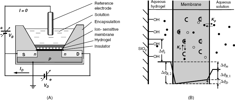
The structure of a neutral ionophore sensing membrane is shown in Figure 11.13B. As is typical of potentiometric ion sensors, the analyte ion first undergoes partition between the solution and the membrane, followed by recognition by the receptor, with the characteristic constants Kp and Kr, respectively. Potential distribution across the system is shown at the lower part of this figure, where ![]() and
and ![]() are boundary potentials,
are boundary potentials, ![]() is the diffusion potential across the membrane,
is the diffusion potential across the membrane, ![]() is the membrane potential, and
is the membrane potential, and ![]() is the surface potential at the semiconductor/hydrogel interface. The membrane potential is, therefore:
is the surface potential at the semiconductor/hydrogel interface. The membrane potential is, therefore:
(11.21) ![]()
where ![]() is dependent on the analyte concentration while
is dependent on the analyte concentration while ![]() is held constant by the buffer solution in the hydrogel layer. By analogy with Equation (11.18) the threshold voltage of the ISFET can be formulated as follows:
is held constant by the buffer solution in the hydrogel layer. By analogy with Equation (11.18) the threshold voltage of the ISFET can be formulated as follows:
(11.22) ![]()
where Er is the reference electrode potential including the junction potential. Each term in this equation is a constant, except the membrane potential, that depends on the analyte ion activity as shown in section 10.8.3. Upon making appropriate substitutions and rearrangements, one obtains the following response equation in terms of gate voltage at constant drain current:
(11.23) ![]()
where ai is the activity of the analyte ion and z is its charge. The effect of interference by other ions (j) on the response to the analyte ion is accounted for by a Nikolskii–Eisenman-type equation in which ![]() is the potentiometric selectivity coefficient:
is the potentiometric selectivity coefficient:
Hence, the potentiometric ISFET response to ion activity is similar to that of a standard potentiometric ion sensor. In practice, the sensitivity factor can deviate from the theoretical value and should be determined by calibration along with the constant term.
Polymeric ion-sensitive layers can be formed by solvent casting of PVC membranes (with incorporated ionophore and a lipophilic ion) on top of the gate insulator layer. However, cast membranes display poor adhesion and some kind of covalent grafting to the insulator layer imparts much better adhesion. In order for the membrane potential to affect the drain current, the sensing membrane should be extremely thin. For a PVC membrane, this limits drastically the lifetime because of fast leaching of the membrane components into the aqueous solution. Better results have been obtained with polysiloxane membranes prepared in situ by condensation, hydrosilylation or photopolymerization. The membrane is covalently attached to the gate oxide by silanisation of the silanol groups at the gate oxide surface, to introduces methacryl functionalities.
The best sensor stability has been obtained by covalent grafting of both the ion receptor and the lipophilic ion to the polymer network. In this way, the lifetime of the sensor can be extended up to half a year or more.
An alternative to ionophore-based polymeric membranes is the use of molecularly imprinted polymers [23, 24]. Polymerization can be conducted in situ so as to allow covalent bonds to form between the gate insulator oxide and the growing polymer layer. Both organic and inorganic polymers can be imprinted for the purpose of ion sensing. Thus, organic anion FET sensors have been obtained by imprinting the analyte in an inorganic TiO2 polymer formed by sol-gel chemistry over the SiO2 gate insulator [25].
Solid, ion-sensitive membranes (for example, a AgCl–AgBr mixture) can be produced over the gate insulator by vapor deposition to obtain an ISFET responsive to Ag+, Cl− and Br−. In the search for better selectivity, chalcogenide glass materials have been found to perform very well as sensing membranes in ISFETs [26]. A chalcogenide glass film can be formed over the gate insulator by physical vapor deposition in which preformed glass serves as a source of vapors. However, this method yields a glass film with a stoichiometry different from that of the original material. This disadvantage is circumvented by using pulsed laser vapor deposition. In this method, a pulsed laser beam is focused on the glass target in order to produce vapors that are deposited onto the gate insulator. The main advantages of this method are the well-defined reproduction of the stoichiometry of the glass coating and the short process times, as well as the possibility of carrying out the process in a reactive atmosphere.
Chalcogenide glass ISFETs for determining Ag+, Cd2+, Cu2+, Hg2+, Pb2+ with a near-Nernstian response (according to Equation (11.24)), and a detection limit in the μM region, have been developed.
The main advantage of the chalcogenide glass approach lies in the possibility of manufacturing ion sensors by using microfabrication technology, with no need for additional chemical processing. Compared with polymeric membranes, chalcogenide glass membranes display good chemical durability and excellent lifetimes. Their small size allows development of sensor arrays for multicomponent analysis of complex samples. The main drawback of chalcogenide glass membranes is their relatively poor limit of detection that cannot match that of the ionophore-based polymer membranes.
11.2.5 Light-Addressable Potentiometric Sensors (LAPS)
A typical ISFET architecture is derived from that of a FET device and no current crosses the semiconductor body. In contrast, a LAPS is formed out of a simple semiconductor-insulator-sample system [27–29]. The response is generated by infrared light irradiation that produces a photocurrent controlled by the bias voltage.
A LAPS consists of a piece of doped semiconductor coated with an insulator and a chemically sensitive layer in contact with the sample solution (Figure 11.14A). A bias voltage VB is applied to the solution phase via a reference electrode and the circuit is completed with an AC amperometer. If the bias voltage VB is set so as to repel the majority carriers from the layer under the insulator, a depletion layer forms and the DC current across the circuit is negligible. When silicon absorbs light of appropriate wavelength, electron–hole pairs are generated. Under the effect of the electric field, electrons move to the silicon/insulator surface and holes accumulate towards the silicon bulk. This charge separation causes a capacitively coupled displacement of charges in the external circuit. As a result, a transient photocurrent Iph appears that the amperometer can detect. In practice, the light source (a light-emitting diode) is modulated as shown in Figure 11.14B to induce an AC photocurrent. If the bias voltage is too low, the depletion layer cannot form and the photocurrent is zero. However, with increasing bias voltage, the photocurrent increases until it attains a limiting value (Figure 11.14C).
Figure 11.14 (A) The configuration of a light-addressable potentiometric sensor (LAPS); (B) time variation of light intensity and photocurrent; (C) the alternating photocurrent as a function of the bias voltage for a pH LAPS.
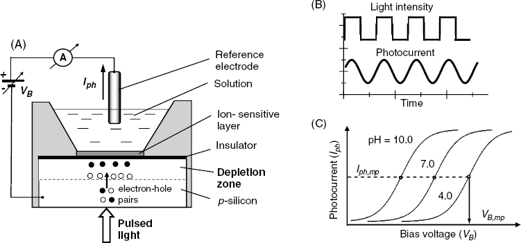
As the bias voltage is in series with the membrane potential, this causes the Iph–VB curve to shift in response to a change in the analyte concentration. This is exemplified in Figure 11.14C for the case of a pH sensor. The mid-point on the Iph–VB curve yields a particular VB,mp value that is related to the logarithm of analyte concentration by means of a linear equation [30].
The light beam can be focussed so as to excite only a limited portion of the silicon body. Therefore, the response is specific to a limited area over the insulator. This allows facile multiplexing by installing a series of different sensing areas, each of them being specific to a particular analyte. Sequential interrogation of each sensing area by a light beam provides the response values necessary for multiple analyte determination.
The redox potential can be measured by coating metallic gold over the insulator layer. In this case, the photocurrent is modulated by the redox potential that builds up at the metal layer according to the Nernst equation.
The volume of sample-solution needed in LAPS operation can be 100 nL or less, which makes the LAP suitable for microchemical analysis.
LAPS devices can be coupled with enzymes that produce either pH or redox-potential change. Combined with the very low sample volume and the multiplexing capability, this makes LAP devices attractive for applications in enzyme-linked immunoassay.
11.2.6 Reference Electrodes for ISFET Sensors
In order to take advantage of the small size of the ISFET sensor, equally small reference electrodes are needed. Moreover, it is desirable to make available a FET-type reference element that can be integrated with the sensor on a single-chip device. As shown previously (Section 11.2.3) an Ag/AgCl reference electrode can be readily integrated with the sensor. However, its proper functioning is dependent on the presence of a chloride salt dissolved in a hydrogel coating. Hence, the lifetime of such electrodes is limited by chloride leakage and contamination with sample ions.
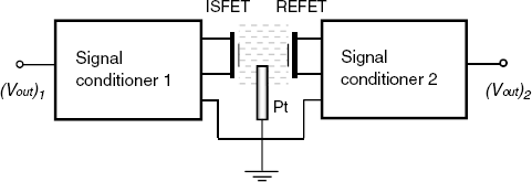
An ideal way to overcome this problem would be to develop a reference FET device (REFET) that, in contact with the solution, does not interact with the ions at all. The REFET and the ISFET can be integrated and connected as shown in Figure 11.15. In this arrangement, grounding of the test solution is performed by a pseudoreference electrode that can be a platinum layer integrated with the ISFET. The potential of the pseudoreference electrode manifests itself as a common signal in the differential system and its possible fluctuations are not disturbing. Each of the ISFETs and REFETs is connected to a signal conditioner that provides an output voltage. The output voltages are fed to the inputs of a differential amplifier that provides at the output a voltage difference that depends on the analyte concentration c:
(11.25) ![]()
In this way, a totally solid-state probe, including both the sensor and the reference element, can be constructed.
Figure 11.15 Block diagram of a differential ISFET/RFET measuring system.
As the most common ion in aqueous samples is the hydrogen ion, an ideal REFET should not be responsive to this ion. So, in principle, a REFET can be obtained by coating a compact hydrophobic polymer membrane (for example, Teflon) over the gate insulator. Rather than their hydrophobicity, it is its very low surface buffer capacity that makes such membranes suitable for REFET applications.
If the sample pH is controlled by a buffer system, a pH FET sensor can function as the reference element. Thus, in enzymatic FET sensors, the reference element can be a pH ISFET sensor coated with a membrane with no enzymatic activity.
11.2.7 Enzymatic FET Sensors (EnFETs)
An enzymatic ISFET sensor can be obtained by coating an enzyme layer over the insulator in a pH ISFET [31]. Clearly, this approach works well with enzymes that produce a change in pH on conversion of the substrate. Principally, this approach is similar to that already introduced in the Section 10.18. In the first approach of this type, penicillinase was used to develop a penicillin sensor [32]. However, the change in the pH can affect the enzyme activity and, in addition, the products of the reaction can be poorly dissociated acids or bases. In such a case, amount of H+ or OH– ions produced per mole of converted substrate also depends on pH. Such factors, which are also present in the case of enzymatic potentiometric sensors, cause the response to be nonlinear.
Such problems can be alleviated by operating the sensor under pH-static conditions [33]. As in the case of the CO2 probe introduced previously, a noble-metal electrode is included closely around the ISFET gate area. This electrode produces either hydrogen or hydroxyl ions by water electrolysis. By a feedback from the pH sensor, the electrolysis current is regulated so as to keep the pH at a constant level. This current is therefore proportional to the rate of product formation, independently of the buffer capacity of the system. The current response varies linearly with substrate concentration, as is typical of a enzymatic sensor with the response proportional to the product concentration.
In addition to the EnFET approach, an enzymatic FED sensor can be designed as a LAPS or capacitor-type sensor. For the particular case of penicillin sensors, it was shown that all three of the above devices give similar performances [34]. Selection of a particular approach should be made by taking into account the complexity of the readout equipment the sensor configuration and the available manufacturing technology with regard to the particular application to be addressed.
The performances of capacitive FED sensors are considerably improved by using a porous surface silicon body upon which the insulator layer is formed by chemical vapor deposition, as shown in Figure 11.16. Deposition of the enzyme layer over the porous insulator layer allows for higher enzyme loading and, in this way, enhances the durability of the device. At the same time, the higher surface area brings about an increased capacitance, which is advantageous from the standpoint of response measurement [35]. Nonmodified porous insulator surfaces proved to give superior performances in pH detection.
Figure 11.16 A porous EIS structure for FED sensors. The porous silicon surface is formed by anodic electrochemical etching. Adapted with permission from [10]. Copyright 2001 John Wiley & Sons Ltd.
Further advances in EnFET technology aim at expanding the response range, lowering the limit of detection and improving the design of multiplexed EnFET sensors [36, 37].
11.2.8 Outlook
FED ion sensors are developed from semiconductor-insulator structures by adding a responsive layer over the insulator instead of the metal gate, which is replaced with a reference electrode. A potential difference formed in response to the analyte interaction with the responsive layer determines a modification in a characteristic electrical parameter of the device. This modification arises from the alteration of the device threshold voltage.
There are three possible approaches to the design of FED ion sensors, namely the EIS ion-sensitive capacitor, the ISFET and the LAPS. EIS capacitor sensors rely on the shift of the capacitance–voltage curve due to the ion interaction with the device. In the case of ISFETs, it is the shift of the drain current–gate voltage that provides the sensor response. In contrast to the above two designs, which involve only electrical devices, the LAPS resorts to light in order to excite a photocurrent that depends on the electric potential at the device/solution interface. The feasibility of each of the above type of sensor is well documented and an option for a particular approach is determined mostly by the complexity of the measurement setup. Although the LAPS seems to be more intricate, it offers an important advantage in the case of sensor multiplexing. This is due to the fact that a LAPS can be build up on a single EIS structure on which a series of different sensitive layers can be formed. The response of each layer is obtained by scanning the device with a light beam.
The most straightforward application of FED device sensors is represented by the pH sensors in which the sensing layer is formed by ionogen groups at the insulator surface. FED pH sensors can function as transducers in gas probes for detecting gases that modify by dissolution the local pH. On the other hand, upon adding an enzymatic layer to a FED pH sensor, one can obtain a FED biocatalytic sensor. Ion-sensitive FED devices are fabricated by including an ion-responsive membrane, either in the solid-state form or as a polymeric membrane. Ion-responsive membranes used in FED ion sensors are, in general, similar to those developed in the frame of potentiometric ion sensors. When using polymer membranes, care should be taken to secure a stable potential difference between the membrane and the insulator.
The most attractive feature of FED sensors is the easy manufacturing by microfabrication technology. Taking also into account the small size of the device, it results that FED ion sensors and biosensors are suitable for multiplexing in order to obtain multisensor arrays, which, in addition to chemical sensors, can also include sensors for physical parameters.
An instructive survey of various kinds of FED ion sensors and biosensors is presented in ref. [34].
11.3 FED Gas Sensors
As pointed out before, a key parameter of the functioning of field effect devices is the threshold voltage, which depends on the difference between the work function of the metal and that of the semiconductor. Upon interaction of a gas with either the metal or the semiconductor the work function of the sensing pertinent part of the device can be altered [5,38]. The resulting change in the threshold voltage can be measured and used to calculate the gas-analyte content in a gas mixture.
11.3.1 FED Hydrogen Sensors
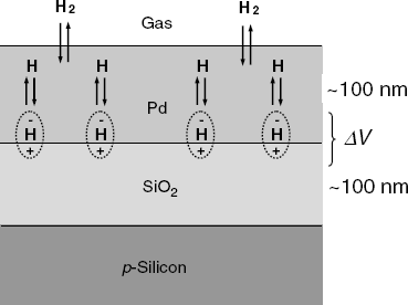
Metal-oxide-semiconductor layered structures respond to the hydrogen concentration in a gas if the metal layer consists of palladium or platinum. The general structure of such a sensor is shown in Figure 11.17. The response mechanism is based on the catalytic properties of the platinum metal which can absorb molecular hydrogen from the gas sample and promotes molecule dissociation to hydrogen atoms dissolved in the bulk of the metal. Further, hydrogen atoms undergo fast diffusion through the metal and reach the metal/oxide interface. Hydrogen atoms adsorb at the interface and turn polarized, forming a dipoles layer. This layer generates a potential difference across the interface that affects the charge distribution at the semiconductor surface. As a consequence, the electrical parameters of the MIS system are altered in relation to hydrogen concentration in the gas sample [4, 39, 40]. The surface dipoles modify the work function of the metal with an amount that is the electrical work required to transfer an electron throughout the dipolar layer on its way out of the metal.
Figure 11.17 Structure of a Pd-SiO2-p-silicon MIS hydrogen sensor.
Therefore, the response to hydrogen can be interpreted by taking into account the effect of the work function on the threshold voltage. The first hydrogen sensor based on this principle was developed by Lundström in 1975 [40]. A retrospective overview of the development of MIS gas sensors is presented in refs. [42, 43].
Two alternative types of FED gas sensor are possible, namely the MIS capacitor type and the MISFET type (Figure 11.18). The MISFET-type sensor is often called ChemFET, an acronym for chemically sensitive field-effect transistor. In both devices, the 100–200-nm thick palladium layer functions as analyte-sensing element. In the case of the capacitor device, the response signal is the change in the bias voltage needed to keep the capacitance at a constant value (Figure 11.18A). As is typical of MIS capacitors, the capacitance–voltage curves are obtained by AC current measurements.
Figure 11.18 FED hydrogen sensors and corresponding characteristic curves.
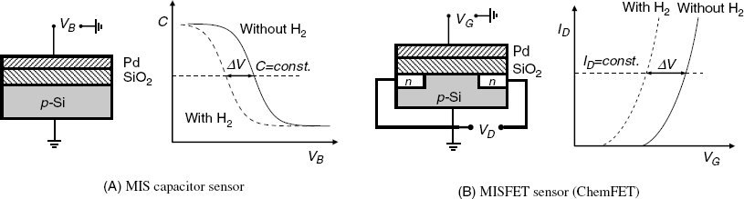
The structure of a MISFET sensor is more intricate, but the operation of this device involves only DC signals. As shown in Figure 11.18B, the change in the threshold voltage produced by hydrogen absorption induces a shift of the drain current–gate voltage curve at a constant drain current. The operation of this sensor is therefore similar to that of the ion-sensitive FET devices.
With both MIS capacitors and MISFET sensors the response is determined by the alteration of the threshold voltage. In turn, the change in the threshold voltage depends of the amount of gas absorbed in the metal phase at equilibrium with the gas phase. Further, the concentration of the gas in the metal is determined by the partition coefficient in the gas–metal system, which is defined as follows:
(11.26) ![]()
The response function in terms of voltage change (![]() in Figures 11.18A and B, respectively) is the same for both the MIS capacitor and the MISFET sensor. Denoting by VT,H and VT,0 the threshold voltage in the presence of or in the absence of hydrogen, respectively, the measured voltage change is:
in Figures 11.18A and B, respectively) is the same for both the MIS capacitor and the MISFET sensor. Denoting by VT,H and VT,0 the threshold voltage in the presence of or in the absence of hydrogen, respectively, the measured voltage change is:
(11.27) ![]()
The response function that relates the voltage change to the hydrogen content can be approximated by the Langmuir isotherm equation as follows [43]:
where ![]() is the partial pressure of hydrogen while
is the partial pressure of hydrogen while ![]() and
and ![]() are empirical parameters. At very low partial pressure, Equation (11.28) can be reduced to the following linear function:
are empirical parameters. At very low partial pressure, Equation (11.28) can be reduced to the following linear function:
(11.29) ![]()
Here, the proportionality constant ![]() includes the effect of oxygen, if oxygen is present in the sample. Therefore, the calibration and the measurement should be performed at a similar oxygen content in the standard gas and the unknown sample.
includes the effect of oxygen, if oxygen is present in the sample. Therefore, the calibration and the measurement should be performed at a similar oxygen content in the standard gas and the unknown sample.
The response time of the sensor is determined by the rate of hydrogen diffusion within the palladium layer. As this process is very fast even at the room temperature, the response time under these conditions is of about 0.15 ms. The response time can be dropped to about 10 μs by operating the device at 150 °C.
The reported limit of detection of MIS hydrogen sensors is close to 3 × 10⁻⁵ Pa hydrogen partial pressure in an inert atmosphere and 5 × 10⁻⁴ Pa in air. The higher detection limit in air is due to oxygen interference. Oxygen and hydrogen react at the metal surface to form water and, in this way, hydrogen atoms are depleted in the metal surface layer. Consequently, the hydrogen atom concentration in the metal is reduced.
More details about the response mechanism of MIS hydrogen sensors can be found in ref. [43].
11.3.2 Metal Gate FED Sensors for Other Gases
Ammonia can also be detected by a palladium-layer MIS device. Ammonia molecules dissociate under the catalytic effect of the metal producing hydrogen atoms that are detected according to the previously emphasized mechanism. In order to achieve a reasonable sensitivity, the sensor should be operated a temperature over 100 °C in order to promote the dissociation. Sensitivity to ammonia can be enhanced by adding an about 3-nm layer of a catalytic metal (Pt or Ir) over the Pd layer. In this version, the operation temperatures can be only slightly above room temperature and can be used to monitor enzymatic reactions that evolve ammonia.
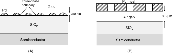
Palladium MIS devices are also responsive to other gases such as carbon monoxide, hydrogen sulfide, alcohols, amines and unsaturated hydrocarbons. However, as such gases are poorly soluble in palladium, relatively few molecules reach the metal/semiconductor interface to form a dipole layer. Hence, the sensitivity of a sensor in a configuration like that in Figure 11.17 is poor when above gases are concerned. A reasonable sensitivity can be achieved by means of a discontinuous palladium gate (Figure 11.19A). In this case, gas molecules adsorb at the triple phase boundary formed by the gas, the insulator and the metal spots. As a result, the effect of the gas on the work function of the metal is much greater than in the case of a compact metal layer.
Figure 11.19 Alternative configurations of MIS gas sensors. (A) Discontinuous metal gate; (B) suspended-gate MIS sensor.
The detection limit for the above-mentioned gases is generally of the order of 1 ppm in air. The response function of the sensor is given in Equation (11.30) where pG is the partial pressure of the analyte whilst ![]() and a are empirical parameters.
and a are empirical parameters.
An alternative approach to sensing palladium-insoluble gases relies on devices including a suspended metal gate that is not in direct contact with the insulator surface. The suspended gate can be a metal mesh (Figure 11.19B), a perforated metal plate or, in general, a metal plate mounted so as to allow communication between the air gap and the gas sample. The air gap between the gate and the insulator functions as an additional insulator layer. When polar gas molecules adsorb either at the metal or the insulator surface, the molecular dipoles give rise to a surface potential that is proportional to the density of adsorbed molecules. This potential difference is in series with the gate voltage and, therefore, alters the drain current. A suspended-gate FED sensor can be produced by microfabrication, with the gate made of heavily doped silicon, which is an electronic conductor [44]. In an alternative design, the solid insulator is absent and the single present insulator is the air gap. In this instance, the analyte gas can adsorb on the semiconductor surface and affect directly the charge transport through the channel.
Not only metals, but also other conductive materials can be used to fabricate the suspended gate. The gate material should be selected so as to be able to interact with the analyte. For example, Figure 11.20 shows a humidity sensor including a polycrystalline silicon suspended gate. The gate has been obtained by chemical vapor deposition over a preformed siloxane layer that has been removed after completing the deposition.
Figure 11.20 Scanning electron microscope image of a suspended gate FET device. The device area is 130 μm × 70 μm. Reproduced with permission from [46]. Copyright Elsevier 2010.
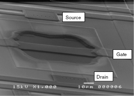
As shown before, a catalytic metal gate FED sensor can respond to a broad variety of different gases. That is why it is important to underline several methods for controlling the selectivity of these sensors. A straightforward method relies on the control of the operation temperature that affects both the rate of chemical reactions and the partition coefficient of the gas. On the other hand, one can resort to a particular catalytic metals or alloy as the gate materials in order to obtain convenient selectivity.
Due to the very small size, MIS gas sensors are suitable for the fabrication of sensor arrays. An array can be formed of several sensors, each of them responding selectively to a certain analyte. As advanced selectivity is hardly achievable, it is more convenient to make use of an assembly of cross-selective sensor and extract the concentration of each analyte by multivariate data analysis (Section 1.7). This approach is also suitable in the design of electronic nose devices [46].
In many industrial applications the gas sensor should operate at a high temperature. Under such conditions the semiconductor properties of silicon are altered due to the relatively low bandgap of this material. High-temperature MIS gas sensors rely on semiconductor with a wide bandgap, such as silicon carbide [47], group III element nitrides (AlN, GaN) and semiconductor diamond.
In conclusion, catalytic metal gate FED gas sensors are very convenient for monitoring hazardous gases in industrial environment and also for the fabrication of gas-sensor arrays.
11.3.3 Organic Semiconductors as Gas-Sensing Materials
The application of metal gate FED gas sensors is mostly limited to the detection of hydrogen and certain hydrogen-containing gases and vapors. This limitation arises from the catalytic nature of the gas interaction with the metal gate. Conversely, organic semiconductors provide a broader variety of possible interactions with gases and vapors and are well suited for detecting polar molecules. Both the sensitivity and the selectivity of organic semiconductor sensors can be tuned by doping or by proper tailoring of certain components of the device. As in the case of the metal gate ChemFETs, the transduction mechanism relies on the modification of the work function of the sensing material.
Two kinds of materials have been used for sensing purposes in organic semiconductor gas sensors, namely molecular semiconductors (phthalocyanines and porphyrins) and conducting polymers [48].
Phthalocyanines and porphyrins have been already introduced in Section 10.9.9. Both kinds of compound consist of macrocycles including four pyrrole units and features a conjugated ![]() -bond system that is responsible for the semiconducting properties. At the same time, the four pyrrole nitrogens can form coordination bonds with various metal ions. In the solid-state form, such planar molecules form molecular stacks and can accommodate dopant molecules in channels adjacent to the stacks. Metal phthalocyanines can be obtained either as insulators (for example, NiPc; Pc stands for phthalocyanine) or intrinsic p-semiconductors (for example, LuPc2). Insulator phthalocyanines are easily converted into p-semiconductors by doping.
-bond system that is responsible for the semiconducting properties. At the same time, the four pyrrole nitrogens can form coordination bonds with various metal ions. In the solid-state form, such planar molecules form molecular stacks and can accommodate dopant molecules in channels adjacent to the stacks. Metal phthalocyanines can be obtained either as insulators (for example, NiPc; Pc stands for phthalocyanine) or intrinsic p-semiconductors (for example, LuPc2). Insulator phthalocyanines are easily converted into p-semiconductors by doping.
Depending on the properties of the analyte gas, the phthalocyanine–analyte interaction can proceed according to various mechanisms. Thus, by interaction with the metal center, an oxidizing species generates extrinsic positive charges, while a reducing species gives rise to negative charges. That is why phthalocyanine films are suitable for the detection of oxidizing gases such as ozone and nitrogen dioxide. Weak charge-transfer interactions with the organic region of the molecule are relevant in the case of analytes that do no interact with the metal ion.
Phthalocyanine sensing films can be obtained by vapor deposition or by the Langmuir–Blodgett technique. Sensors based on phthalocyanine can operate at temperatures up to 200 °C. Phthalocyanine applications in FED gas sensors has been reviewed in ref. [49].
Conducting polymers, (introduced in Section 5.9) can be deposited by spin coating, drop casting or electrochemical polymerization. The cast layer incorporates an important proportion of solvent. Hence, by solvent evaporation, the properties of the film are altered. A better alternative relies on gel-like films formed of a mixture of polymer and an ionic liquid. Ionic liquids are salts of certain organic cations and are present in the liquid state at ambient temperature. Low volatility, good thermal stability and good solubility of gases of ionic liquids result in superior performances over the solid polymer coatings.
Sensitivity improvement can be achieved by incorporating binding sites into the polymer coating. Binding sites can be formed of dielectric polymers, carbon fibers, metal nanoparticles or metal oxides.
Conducting polymer gas sensors can be operated at temperatures up to 90 °C.
11.3.4 Organic Semiconductors FED Gas Sensors
Organic semiconductors are suitable as sensing materials in gas sensors and allow potentiometric sensors for neutral molecules to be devised based on the modulation of the work-function. In order to perform this task, an organic semiconductor should be integrated within a field effect device. There are two possible integration alternatives. The first one relies on inorganic semiconductor FED devices in which the gate is made of an organic semiconductor, as shown in Figure 11.21A. This is actually a modified ChemFET device. Upon gas interaction with the organic sensing layer, the work-function difference between the semiconductor and the gate is altered and the threshold voltage changes in relation to the gas concentration.
Figure 11.21 Two types of gas sensors including an organic semiconductor (OS) sensing layer. (A) Modified gate silicon FET (ChemFET); (B) organic semiconductor transistor (OFET). Dashed arrows indicate the current flow through the device.
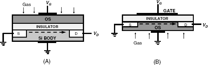
Another approach is based on organic field-effect transistors (OFET, Figure 11.21B). An OFET has the typical configuration of MISFETs but are fabricated as thin-film transistors, which implies that the thickness of the semiconductor body is very low [51–53]. Gas interaction with the organic semiconductor does modify the threshold voltage of the device, which makes OFET suited for gas-sensing applications [53].
There is, however, an essential difference between the organic layer ChemFET sensor and the OFET-type one. In the first case, no current flows through the organic layer, whereas in the second case, the current passes from the source to the drain throughout the organic semiconductor and encounters three resistances: two at the contacts and one in the organic semiconductor. The change in the work function can affect each of these three resistances. If a voltage is applied to the gate (Figure 11.21B) this will affect not only the drain current, but also all these resistances. Hence, the response is nonlinear. It was therefore asserted that the OFET device acts actually as a chemically modulated resistor and the field effect modulation of the current is of a minor importance [48].
OFET application in gas sensors is still in its infancy. Conversely, modified gate ChemFET sensors are well-established devices. In addition to the organic semiconductor approach underlined in Figure 11.21A, modified suspended-gate devices are also of interest. In this case, the sensing layer is supported on a metal gate separated from the insulator by an air gap.
Thus, an alcohol vapor sensor has been obtained by depositing a polypyrrole sensing layer over a platinum mesh suspended gate [54]. Figure 11.22A shows the structure of and NO2 sensor based on a 150–200-nm thick phthalocyanine sensing layer. This layer has been produced by spraying from polyacrylic acid solutions onto gold-patterned alumina through a mechanical mask. In addition to the measuring unit, the device includes reference units for humidity and drift compensation. Humidity compensation is important because organic semiconductors respond in general to the content of water vapors in the gas sample. The graph in Figure 11.22B demonstrates a linear response in a semilogarithmic representation and also proves the very good reproducibility of the results.
Figure 11.22 (A) Structure of a suspended-gate copper phthalocyanine (CuPc) based FET nitrogen dioxide sensor SG indicates the suspended gate on which the phthalocyanine layer is loaded. (B) The calibration graph of a sensor like that in A at 25 °C. Reproduced with permission from [56]. Copyright 2006 Elsevier.
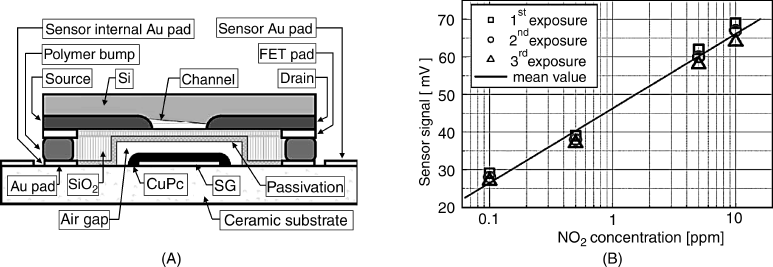
11.3.5 Response Mechanism of FED Gas Sensors
In the case of potentiometric ion sensors, the key parameter is the surface potential that forms in response to the ion transfer between a solution and a semipermeable membrane. The transfer process involves the transfer of an integer number of elementary charges that are borne by each ion.
The situation is radically different when a polar molecule A enters a metal or semiconductor material. This becomes polarized, which is similar to the transfer of a partial charge![]() , where e is the elementary charge and
, where e is the elementary charge and ![]() is a fractional number:
is a fractional number:
where ![]() is the equilibrium constant for the gas dissolution in the solid material,
is the equilibrium constant for the gas dissolution in the solid material, ![]() is the partial pressure of the gas A and
is the partial pressure of the gas A and ![]() is the absorption coefficient in the Henry isotherm. Hence, the
is the absorption coefficient in the Henry isotherm. Hence, the ![]() product is the concentration of the dissolved gas in the solid phase.
product is the concentration of the dissolved gas in the solid phase.
If ![]() , reaction (11.31) would represent the formation of a charge-transfer complex between the solid matrix and the dissolved gas. Assuming that the matrix is a semiconductor and the gas is an electron donor (that is, a Lewis base), a negative charge is transferred to the conduction band. For an electron-acceptor gas (that is, Lewis acid), electrons are withdrawn from the conduction band thus increasing the hole density. Such processes can be viewed as doping processes that shift the Fermi level. Consequently, the work function of the matrix material is altered.
, reaction (11.31) would represent the formation of a charge-transfer complex between the solid matrix and the dissolved gas. Assuming that the matrix is a semiconductor and the gas is an electron donor (that is, a Lewis base), a negative charge is transferred to the conduction band. For an electron-acceptor gas (that is, Lewis acid), electrons are withdrawn from the conduction band thus increasing the hole density. Such processes can be viewed as doping processes that shift the Fermi level. Consequently, the work function of the matrix material is altered.
Based on these premises, an equation relating the Fermi level of an n-semiconductor to the partial pressure of the donor gas has been derived in the following form [38]:
where ![]() is the Boltzmann constant and T is the absolute temperature. The constant term
is the Boltzmann constant and T is the absolute temperature. The constant term ![]() is the standard donor-dopant energy level at
is the standard donor-dopant energy level at ![]() , that is, in the pure analyte gas. For a p-type semiconductor, the term
, that is, in the pure analyte gas. For a p-type semiconductor, the term ![]() should be replaced by the standard acceptor-dopant energy level
should be replaced by the standard acceptor-dopant energy level ![]() . Equation (11.32) has been derived under the assumption that the equilibrium constant
. Equation (11.32) has been derived under the assumption that the equilibrium constant ![]() is not affected by gas absorption, which is only an approximation. Despite this limitation, Equation (11.32) represents a sound basis for the rationalization of the response of semiconductor-based sensors to neutral molecules.
is not affected by gas absorption, which is only an approximation. Despite this limitation, Equation (11.32) represents a sound basis for the rationalization of the response of semiconductor-based sensors to neutral molecules.
There is a striking analogy between Equation (11.32) and the Nernst equation that applies to electron or ion transfer between two phases. The analogy is more evident if one remember that ![]() and
and ![]() , where
, where ![]() is the Avogadro number and F is the Faraday constant. The main difference originates from the charge term in the denominator of the prelogarithm term. While the charge z in the standard Nernst equation is an integer number, the term
is the Avogadro number and F is the Faraday constant. The main difference originates from the charge term in the denominator of the prelogarithm term. While the charge z in the standard Nernst equation is an integer number, the term ![]() in Equation (11.32) is a fractional number.
in Equation (11.32) is a fractional number.
The change in the Fermi level of the sensing material can be assessed by means of the change in the threshold voltage of a FED including a semiconductor-based sensing layer. An important point is that the change in the threshold voltage can be observed only if the gas-sensitive coating interface is capacitive, that is, if no interphase electron transfer is possible [38]. This implies that the alteration of the work function originates only in the sensing layer adjacent to the insulator. Thus, in the case of the hydrogen sensitive Pd-ChemFET, the formation of a dipole layer at the Pd insulator interface is responsible for the local modulation of the work function.
Sensor operation in the saturation regime (![]() ) is preferable because it implies an explicit relationship between the work function and the operating gate voltage. Using Equation (11.7) one obtains the following relationship between the gate voltage and the work function at constant drain current:
) is preferable because it implies an explicit relationship between the work function and the operating gate voltage. Using Equation (11.7) one obtains the following relationship between the gate voltage and the work function at constant drain current:
(11.33) ![]()
On the other hand, the dependence of the gate voltage on the partial pressure of the analyte gas (pA) can be formulated as follows [48]:
(11.34) ![]()
where ![]() includes all constant terms related to the transistor and the sensing layer as well as
includes all constant terms related to the transistor and the sensing layer as well as ![]() . pi is the partial pressure of any other gas in the sample and
. pi is the partial pressure of any other gas in the sample and ![]() is the potentiometric selectivity coefficient. The above equation is alike to the Eisenman-Nikolskii equation, with the notable difference that instead of the integer ion charge z, the fractional charge
is the potentiometric selectivity coefficient. The above equation is alike to the Eisenman-Nikolskii equation, with the notable difference that instead of the integer ion charge z, the fractional charge ![]() appears in the prelogarithm factor. The background response
appears in the prelogarithm factor. The background response ![]() , is obtained with a reference gas in which
, is obtained with a reference gas in which ![]() : Therefore, the gate voltage change with respect to the background is:
: Therefore, the gate voltage change with respect to the background is:
(11.35) 
If the interference is negligible, ![]() is proportional to the logarithm of the analyte partial pressure. This kind of response is illustrated in Figure 11.23B.
is proportional to the logarithm of the analyte partial pressure. This kind of response is illustrated in Figure 11.23B.
11.3.6 Outlook
FET gas sensors represent an application of FET devices to sensing of neutral molecules. In contrast to FED ion sensors, which are obtained by forming an ion-responsive layer over the insulator film, FET gas sensors preserve the standard structure of MIS devices. The sensing element in FET gas sensors is a structural component of the MIS devices that is typically the gate.
In order to perform gas recognition, the gate is formed of a metal that can absorb or adsorb the target analyte. In the case of hydrogen sensors, sorption leads to the dissociation of the hydrogen molecules yielding hydrogen atoms. Hydrogen atoms become polarized at the metal/insulator surface and in this way alter the work function of the metal. As a result, the threshold voltage of the MIS device is modified, leading to the modification of a characteristic functioning parameter. In the case of MIS capacitors, this parameter is the capacitance, whilst in the case of a MISFET device, the drain current is modified. This principle has been also applied to FED sensors for gases that give rise to hydrogen atoms upon dissolution in a the gate metal, such as ammonia.
Gas sensing by FED devices is also feasible for gases that are not soluble in the gate metal but undergo adsorption at the gate surface accompanied by molecule polarization. Best performances are obtained in this case by means of suspended-gate devices. Further, modification of the suspended gate with an organic semiconductor film opened the way to the development of FED sensors gas for various gases and vapors that cannot be sensed by a metal gate.
FED gas sensor relies on the formation of polar atoms or molecules upon interaction between the sensing element and the analyte. This process is similar to the transfer of a partial charge between the analyte and the sensing material. Consequently, the sensor response can be described by a generalized form of the Nernst equation, in which a fractional charge replaces the integer charge included in the standard form of this equation.
11.4 Schottky-Diode-Based Gas Sensors
A Schottky diode is formed of a metal film coated over a semiconductor surface to form a heterogeneous metal–semiconductor junction. The Schottky diode is a rectifier, which implies very low resistance under forward bias and very high resistance under reverse-bias conditions.
Gas sensors based on the Schottky diode can be obtained by coating a thin layer of a catalytic metal (for example, palladium) over a semiconductor oxide such as titanium dioxide. The response of this sensor is based on the variation of the work function of the metal upon interaction with the gas [40, 57].
In order to understand the response mechanism of the diode gas sensor it is necessary to examine first the band diagram of the diode in the absence and then in the presence of an analyte like hydrogen. The band diagram of a palladium Schottky diode in an inert atmosphere is shown in Figure 11.23A. The direct contact between the metal and semiconductor leads to equalization of the Femi levels in each component under equilibrium conditions. Due to surface charges, both the conduction and the valence bands in the semiconductor bend upwards. When an electron moves from the metal to the semiconductor, it encounters an energy barrier ![]() that is the difference between the Fermi level and the edge of the conduction band at the interface. The energy barrier is determined by two material properties, namely the work function of the metal (
that is the difference between the Fermi level and the edge of the conduction band at the interface. The energy barrier is determined by two material properties, namely the work function of the metal (![]() ) and the electron affinity of the semiconductor (
) and the electron affinity of the semiconductor (![]() ). By definition, the electron affinity is the energy required to bring an electron from the vacuum level to the bottom of the conduction band at the surface. Therefore, according to the diagram in Figure 11.23A the energy barrier is given by:
). By definition, the electron affinity is the energy required to bring an electron from the vacuum level to the bottom of the conduction band at the surface. Therefore, according to the diagram in Figure 11.23A the energy barrier is given by:
Figure 11.23 Band energy diagram of a palladium–semiconductor system in pure air (A) and in hydrogen-containing air (B). (C) Current–voltage curves of a palladium-semiconductor Schottky diode in the absence or in the presence of hydrogen.
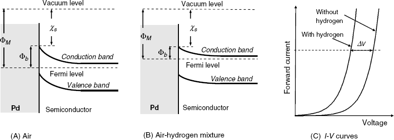
An electron from the metal can move to the semiconductor only if its thermal energy overcomes the energy barrier ![]() . On the other hand, an applied voltage affects the position of the Fermi level in the semiconductor relative to the Fermi level in the metal. As a consequence, the electron flow across the diode is determined by the applied voltage and, under forward-bias conditions the current is given by the following equation [1]:
. On the other hand, an applied voltage affects the position of the Fermi level in the semiconductor relative to the Fermi level in the metal. As a consequence, the electron flow across the diode is determined by the applied voltage and, under forward-bias conditions the current is given by the following equation [1]:
Here, V is the applied voltage, kB is the Boltzmann constant, T is the absolute temperature e is the elementary charge and Ab is a potential barrier-dependent term:
(11.38) ![]()
where kS is constant parameter of the semiconductor. Equation (11.36) indicates that the Ab term depends on the work function of the metal and hence can vary upon hydrogen absorption. Therefore, the forward current increases exponentially with the voltage (Equation (11.37)) and the pre-exponential term depends on the hydrogen partial pressure. As a result, hydrogen absorption causes the current–voltage curve to be translated with respect to the reference curve obtained in an inert atmosphere, as shown in Figure 11.23C. The voltage shift ![]() at a constant current is a function of the partial pressure of hydrogen in the gas sample.
at a constant current is a function of the partial pressure of hydrogen in the gas sample.
The structure of a Schottky-diode hydrogen sensor is shown in Figure 11.24A, whilst the response of Schottky diode to the hydrogen content in air is shown in Figure 11.24B. Data in Figure 11.24B have been obtained with a Pd-TiO2 diode operated at the room temperature. A clear voltage shift at constant forward current can be noted at hydrogen concentrations as low as 10 ppm and the response range extends over a broad interval.
Figure 11.24 (A) A Pd Schottky-diode hydrogen sensor; (B) current–voltage characteristic curves of a Pd-TiO2 Schottky diode at different concentrations of hydrogen in air at 25 °C. Hydrogen concentration: (1) 0 ppm; (2) 14 ppm; (3) 140 ppm; (4) 1400 ppm; (5) 7150 ppm; (6) 1%; (7) 1.5%. (B) Adapted with permission from [58]. Copyright 1980 Elsevier.
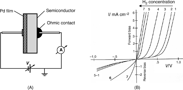
Schottky-diode sensors are very simple and inexpensive devices. As is typical of semiconductor gas sensors, the response is generated by modulation of the work function under the action of the gas analyte. If silicon is used as the semiconductor, Schottky-diode sensors are compatible with monolithic silicon integrated circuit technology. The current–voltage curve obeys an exponential low and exhibit excellent hydrogen detection sensitivity. However, the operation temperature of silicon diodes is limited to 250 °C, due to the small energy gap of the silicon. Sensors operating at higher temperature can be obtained by using semiconductors with a larger energy bandgap, such as silicon carbide or semiconductor diamond.
11.5 Carbon-Nanotube-Based Field-Effect Transistors
Semiconductor nanomaterials, such as graphene, carbon nanotubes and silicon nanowires are currently being intensively investigated for possible applications in microelectronics. It is therefore not surprising that nanomaterial-based semiconductor devices have raised considerable interest from the standpoint of chemical sensing. This section introduces the carbon nanotube field-effect transistor (CNFET) and some of its possible applications in chemical sensors.
As shown in Figure 11.25A, a nanosize field-effect transistor can be constructed by connecting a single-walled semiconductor carbon nanotube to source and drain contacts over an insulating film coated over a conducting material, such as a very highly doped semiconductor. The underlying material functions in this case as a gate, whereas the nanotube forms the channel. The device characteristic curve (that is, the ![]() curve) is similar to that of a standard FET. If a sufficiently negative gate potential is applied, holes are created in the nanotube resulting in increased conductance. However, the manufacturing reproducibility of single-nanotube FETs is poor and, from this standpoint, it is more convenient to use instead a network of randomly oriented nanotubes. Another CNFET device geometry involves suspending the nanotube over a trench to prevent the contact with the substrate and gate oxide. This technique has the advantage of less charge-carrier scattering at the CNT/substrate interface, which improves the device performance.
curve) is similar to that of a standard FET. If a sufficiently negative gate potential is applied, holes are created in the nanotube resulting in increased conductance. However, the manufacturing reproducibility of single-nanotube FETs is poor and, from this standpoint, it is more convenient to use instead a network of randomly oriented nanotubes. Another CNFET device geometry involves suspending the nanotube over a trench to prevent the contact with the substrate and gate oxide. This technique has the advantage of less charge-carrier scattering at the CNT/substrate interface, which improves the device performance.
Figure 11.25 (A) Structure and wiring of a CNFET. (B) A CNFET-based chemical sensor for liquid samples. SWNT stands for single-walled carbon nanotube. Reproduced with permission from [59]. Copyright 2007 Wiley-VCH Verlag GmBH & Co. KGaA.
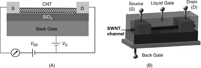
The current across the nanotube channel is very sensitive to the state of the nanotube surface. As a result, adsorption of simple gases such as oxygen or ammonia on the nanotube have a great effect on the source–drain current at constant gate voltage. A CNFET can therefore act as a chemical sensor and this property is manifested not only in the gas phase but also in liquids. In the case of liquids (Figure 11.25B) a second gate (a “liquid gate”) can be created by inserting a reference electrode into the sample solution.
Two different mechanisms can account for the change in the channel conduction when a CNFET interacts with an adsorbed compound. In the first case (Figure 11.26A), electrons from the adsorbate molecules are transferred to the ![]() orbitals of the nanotube leading to partial hole depletion. In order to achieve the same current, the gate voltage needs to be shifted to more negative values compared with the case of a plain surface. Consequently, the characteristic curve is displaced as shown in Figure 11.26A. In the second mechanism (Figure 11.26B), a charged adsorbate gives rise to an electric potential that scatters the charge carriers in the nanotubes and causes the current to become lesser at any particular applied gate voltage.
orbitals of the nanotube leading to partial hole depletion. In order to achieve the same current, the gate voltage needs to be shifted to more negative values compared with the case of a plain surface. Consequently, the characteristic curve is displaced as shown in Figure 11.26A. In the second mechanism (Figure 11.26B), a charged adsorbate gives rise to an electric potential that scatters the charge carriers in the nanotubes and causes the current to become lesser at any particular applied gate voltage.
Figure 11.26 Effect of surface-adsorbed species on the device characteristics. (A) The effect of electron transfer from adsorbate to the nanotube; (B) the effect of charge carriers scattering by the electric potential created by the adsorbate.
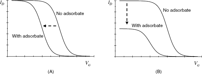
In order to develop a CNFET-based biosensor, it is best to prevent nonspecific interactions by coating the nanotubes with a polymer layer such as polyethylene glycol/polyethyleneimine. A suitable receptor can be attached to this layer in order to achieve analyte binding. A charged analyte molecule (protein or DNA) brings about a decrease in the channel current (Figure 11.26B), which is in relation to the analyte concentration and the incubation time.
Various types of CNFET biosensors based on immunoreceptors, DNA hybridization or enzyme reactions have been reported [59–62]. Because of their submicrometer size CNFET sensors show promising prospects for application in implantable devices for the development of sensor microarrays.
Semiconducting CNTs are very sensitive to gas adsorption, which provides the basis for applications in gas sensors. However, bare CNTs are poorly selective. Selectivity to a particular gas can be secured by suitable modification of the CNT. For example, deposition of palladium nanoparticles causes the conductance of the CNT to vary in the presence of hydrogen. Selectivity to other gases can be obtained using other metal nanoparticles, such as gold, platinum and rhodium. As full selectivity cannot be achieved, it is best to build up an array of gas sensors such as each of them responds to a gas component to a different extent. So, each sensor provides a mixed response but data processing by partial least square regression yields the magnitude of the response to each gas (see Section 1.7). A device of this kind is shown in Figure 11.27. It consists of an assembly of five CNFET formed on a silicon chip. Each device consists of a network of semiconducting CNTs gathered between two metal electrodes (source and gate). CNTs coverage with metal nanoparticles is best achieved by electrochemical deposition such that metal nanoparticles are grown at each predefined site. The response is recorded as the drain current at zero gate voltage. This sensor network allowed selective quantitation of ![]() ,
, ![]() ,
, ![]() and
and ![]() .
.
Figure 11.27 A CNFET gas-sensor array. (A) A silicon chip (2 mm × 2 mm) containing multiple carbon-nanotube devices. (B) Enlarged view of five pairs of metal electrodes connecting networks of CNTs. The first four networks are plated with the metals indicated in figure; the bare device functions as reference element. Reproduced with permission from [63]. Copyright 2006 American Chemical Society.
In conclusion, carbon nanomaterial semiconductor devices provide new possibilities in the design of chemical sensor for both liquid and gaseous samples. Besides CNTs, graphenes are also of interest in the design of FET-type chemical sensors [64].
11.6 Concluding Remarks
The basic principles of semiconductor electronic devices have been successfully applied to develop chemical sensors for both ionic species an neutral molecule compounds. Two main strategies can be distinguished in these applications.
The first strategy relies on a FED structure integrated with a distinct chemically sensitive element, as it occurs in the case of FED ion sensors. Sensing reagents and materials developed in the frame of potentiometric ion sensors area are, in general, suitable for the development of FED ion sensors.
The second strategy relies on field effect devices configured in the standard structure. In this case the analyte interacts with one of the device components, such as the gate or the semiconductor body material. This approach is typical of FED gas sensors. Notwithstanding, certain types of FED gas sensors include a distinct organic sensing layer coated over the gate.
In general, sensing by means of FED devices relies on the alteration of the work function of a metal or semiconductor part of the device.
An important advantage of FED sensors is their compatibility with microelectronics technology that allows mass production in miniaturized format and facile fabrication of sensor arrays.
1. Sze, S.M. and Ng, K.K. (2007) Physics of Semiconductor Devices, Wiley-Interscience, Hoboken, N.J.
2. Blackburn, G.F. (1987) Chemically sensitive field effect transistors, in Biosensors: Fundamentals and Applications (eds A.P.F. Turner, I. Karube, and G.S. Wilson), Oxford University Press, Oxford, pp. 481–530.
3. Huber, R.J. and Janata, J. (eds) (1985) Solid State Chemical Sensors, Academic Press, Orlando.
4. Lundström, I., van den Berg, A., van der Schoot, B.H., and van den Vlekkert, H.H. (1991) Field effect chemical sensors, in Sensors: A Comprehensive Survey (eds W. Göpel, J. Hesse, and J.N. Zemel), Wiley-VCH, Weinheim, pp. 467–528.
5. Oprea A., Bârsan, N., and Weimar, U. (2009) Work function changes in gas sensitive materials: Fundamentals and applications. Sens. Actuators B, 142, 470–493.
6. Bergveld, P., Hendrikse, J., and Olthuis, W. (1998) Theory and application of the material work function for chemical sensors based on the field effect principle. Meas. Sci. Technol., 9, 1801–1808.
7. Zemel, J.N. (1975) Ion-sensitive field effect transistors and related devices. Anal. Chem., 47, 255A–268a.
8. Janata, J. (1985) Chemically sensitive field effect transistors, in Solid State Chemical Sensors (eds R.J. Huber and J. Janata), Academic Press, Orlando, pp. 66–118.
9. Schöning, M.J., Thust, M., Müller-Veggian, M. et al. (1998) A novel silicon-based sensor array with capacitive EIS structures. Sens. Actuators B-Chem., 47, 225–230.
10. Schöning, M.J. and Luth, H. (2001) Novel concepts for silicon-based biosensors. Phys. Status Solidi A-Appl. Res., 185, 65–77.
11. Bergveld, P. (1970) Development of an ion-sensitive solid-state device for neurophysiological measurements. IEEE Trans. Biomed. Eng., BM17, 70–71.
12. Bergveld, P. (1972) Development, operation, and application of ion-sensitive field-effect transistor as a tool for electrophysiology. IEEE Trans. Biomed. Eng., BM19, 342–351.
13. Bergveld, P. (1988) Analytical and bioanalytical applications of ion-selective field-effect transistors, in Comprehensive Analytical Chemistry, vol. 23 (ed. G. Svehla), Elsevier, Amsterdam, pp. 1–172.
14. Bergveld F P. (2003) Thirty years of ISFETOLOGY - What happened in the past 30 years and what may happen in the next 30 years. Sens. Actuators B-Chem., 88, 1–20.
15. Vlasov, Y.G., Tarantov, Y.A., and Bobrov, P.V. (2003) Analytical characteristics and sensitivity mechanisms of electrolyte-insulator-semiconductor system-based chemical sensors - a critical review. Anal. Bioanal. Chem., 376, 788–796.
16. Zhou, D. (2008) Microelectrodes for in-vivo determination of pH, in Electrochemical Sensors, Biosensors, and Their Biomedical Applications (eds X. Zhang, H. Ju, and J. Wang), Academic Press, Amsterdam, pp. 261–305.
17. Korostynska, O., Arshak, K., Gill, E. et al. (2008) Review paper: Materials and techniques for in vivo pH monitoring. IEEE Sens. J., 8, 20–28.
18. Shimada, K., Yano, M., Shibatani, K. et al. (1980) Application of catheter-tip ISFET for continuous in vivo measurement. Med. Biol. Eng. Comput., 18, 741–745.
19. Van der Schoot, B. and Bergveld, P. (1988) Coulometric sensors, the application of a sensor actuator-system for long-term stability in chemical sensing. Sens. Actuators, 13, 251–262.
20. Covington, A.K. (1994) Terminology and conventions for microelectronic Ion-Selective Field-Effect Transistor devices in electrochemistry. Pure Appl. Chem., 66, 565–569.
21. Moss, S.D., Janata, J., and Johnson, C.C. (1975) Potassium ion-sensitive field-effect transistor. Anal. Chem., 47, 2238–2243.
22. Reinhoudt, D.N. (1996) Transduction of molecular recognition into electronic signals. Rec. Trav. Chim. Pays-Bas-J. Roy. Neth. Chem. Soc., 115, 109–118.
23. Suryanarayanan, V., Wu, C.T., and Ho, K.C. (2010) Molecularly imprinted electrochemical sensors. Electroanalysis, 22, 1795–1811.
24. Rao, T.P., Kala, R., and Daniel, S. (2006) Metal ion-imprinted polymers - Novel materials for selective recognition of inorganics. Anal. Chim. Acta, 578, 105–116.
25. Zayats, M., Lahav, M., Kharitonov, A.B. et al. (2002) Imprinting of specific molecular recognition sites in inorganic and organic thin layer membranes associated with ion-sensitive field-effect transistors. Tetrahedron, 58, 815–824.
26. Schöning, M.J. and Kloock, J.P. (2007) About 20 years of silicon-based thin-film sensors with chalcogenide glass materials for heavy metal analysis: Technological aspects of fabrication and miniaturization. Electroanalysis, 19, 2029–2038.
27. Hafeman, D.G., Parce, J.W., and McConnell, H.M. (1988) Light-addressable potentiometric sensor for biochemical systems. Science, 240, 1182–1185.
28. Owicki, J.C., Bousse, L.J., Hafeman, D.G. et al. (1994) The light-addressable potentiometric sensor - principles and biological applications. Annu. Rev. Biophys. Biomolec. Struct., 23, 87–113.
29. Wagner, T. and Schöning, M.J. (2007) Light addressable potentiometric sensors (LAPS): Recent trends and applications, in Electrochemical Sensor Analysis (eds S. Alegret and A. Merkoçi), Elsevier, Amsterdam, pp. 87–128.
30. Adami, M., Sartore, M., Baldini, E. et al. (1992) New measuring principle for LAPS devices. Sens. Actuators B-Chem., 9, 25–31.
31. Shiono, S., Hanazato, Y., and Nakako, M. (1992) Advances in enzymatically coupled field-effect transistors. Methods Biochem. Anal., 36, 151–178.
32. Caras, S. and Janata, J. (1980) Field-effect transistor sensitive to penicillin. Anal. Chem., 52, 1935–1937.
33. Van der Schoot, B.H. and Bergveld, P. (1987) ISFET based enzyme sensors. Biosensors, 3, 161–186.
34. Schöning, M.J. (2005) “ Playing around” with field-effect sensors on the basis of EIS structures, LAPS and ISFETs. Sensors, 5, 126–138.
35. Schöning, M.J., Kurowski, A., Thust, M. et al. (2000) Capacitive microsensors for biochemical sensing based on porous silicon technology. Sens. Actuators B-Chem., 64, 59–64.
36. Schöning, M.J. and Poghossian, A. (2002) Recent advances in biologically sensitive field-effect transistors (BioFETs). Analyst, 127, 1137–1151.
37. Schöning, M.J. and Poghossian, A. (2006) Bio FEDs (field-effect devices): State-of-the-art and new directions. Electroanalysis, 18, 1893–1900.
38. Janata, J. and Josowicz, M. (1998) Chemical modulation of work function as a transduction mechanism for chemical sensors. Accounts Chem. Res., 31, 241–248.
39. Spetz, A., Winquist, F., Sundgren, H. et al. (1992) Field effect gas sensors, in Gas Sensors: Principles, Operation and Developments (ed. G. Sberveglieri), Kluwer, Dordrecht, pp. 219–279.
40. Mandelis, A. and Christofides, C. (1993) Gas-sensitive solid state semiconductor sensors, in Physics, Chemistry, and Technology of Solid State Gas Sensor Devices (eds A. Mandelis and C. Christofides), John Wiley & Sons, New York, pp. 19–132.
41 Lundström, K.I., Shivaraman, M.S., and Svensson, C.M. (1975) Hydrogen-sensitive Pd-gate MOS-transistor. J. Appl. Phys., 46, 3876–3881.
42. Lundström, I., Svensson, C., Spetz, A. et al. (1993) From hydrogen sensors to olfactory images - 20 years with catalytic field-effect devices. Sens. Actuators B-Chem., 13, 16–23.
43. Lundström, I., Sundgren, H., Winquist, F. et al. (2007) Twenty-five years of field effect gas sensor research in Linköping. Sens. Actuators B-Chem., 121, 247–262.
44. Ekedahl, L.-G., Eriksson, M., and Lundström, I. (1998) Hydrogen sensing mechanisms of metal-insulator interfaces. Accounts Chem. Res., 31, 249–256.
45. Mahfoz-Kotb, H., Salaün, A.C., Bendriaa, F. et al. (2006) Sensing sensibility of surface micromachined suspended gate polysilicon thin film transistors. Sens. Actuators B-Chem., 118, 243–248.
46. De Sagazan, O., da Silva Rodrigues, B., Crand, S. et al. (2010) Investigation on suspended gate field effect transistor as humidity sensor. Proc. Eng., 5, 1434–1437.
47. James, D., Scott, S.M., Ali, Z. et al. (2005) Chemical sensors for electronic nose systems. Microchim. Acta, 149, 1–17.
48. Soo, M.T., Cheong, K.Y., and Noor, A.F.M. (2010) Advances of SiC-based MOS capacitor hydrogen sensors for harsh environment applications. Sens. Actuators B-Chem., 151, 39–55.
49. Janata, J. and Josowicz, M. (2009) Organic semiconductors in potentiometric gas sensors. J. Solid State Electrochem., 13, 41–49.
50. Bouvet, M. (2006) Phthalocyanine-based field-effect transistors as gas sensors. Anal. Bioanal. Chem., 384, 366–373.
51. Katz, H.E. (1997) Organic molecular solids as thin film transistor semiconductors. J. Mater. Chem., 7, 369–376.
52. Horowitz, G. (2011) The organic transistor: state-of-the-art and outlook. Eur. Phys. J.-Appl. Phys., 53, Paper 33602.
53. Mabeck, J.T. and Malliaras, G.G. (2006) Chemical and biological sensors based on organic thin-film transistors. Anal. Bioanal. Chem., 384, 343–353.
54. Torsi, L. and Dodabalapur, A. (2005) Organic thin-film transistors as plastic analytical sensors. Anal. Chem., 77, 380A–387A.
55 Josowicz, M. and Janata, J. (1986) Suspended gate field effect transistors modified with polypyrrole as alcohol sensor. Anal. Chem., 58, 514–517.
56. Oprea, A., Weimar, U., Simon, E. et al. (2006) Copper phthalocyanine suspended gate field effect transistors for NO2 detection. Sens. Actuators B-Chem., 118, 249–254.
57. Potje-Kamloth, K. (2008) Semiconductor junction gas sensors. Chem. Rev., 108, 367–399.
58. Yamamoto, N., Tonomura, S., Matsuoka, T. et al. (1980) Study on a palladium-titanium oxide Schottky diode as a detector for gaseous components. Surf. Sci., 92, 400–406.
59. Allen, B.L., Kichambare, P.D., and Star, A. (2007) Carbon nanotube field-effect-transistor-based biosensors. Adv. Mater., 19, 1439–1451.
60. Kichambare, P.D. and Star, A. (2007) Biosensing using carbon nanotube field-effect transistors, in Nanomaterials for Biosensors (ed. C. Kumar), Wiley-VCH, Weinheim, pp. 1–26.
61. Gruner, G. (2005) Carbon nanotube transistors for biosensing applications. Anal. Bioanal. Chem., 384, 322–335.
62. Tarakanov, A.O., Goncharova, L.B., and Tarakanov, Y.A. (2010) Carbon nanotubes towards medicinal biochips. Wiley Interdiscip. Rev.-Nanomed. Nanobiotechnol., 2, 1–10.
63. Star, A., Joshi, V., Skarupo, S. et al. (2006) Gas sensor array based on metal-decorated carbon nanotubes. J. Phys. Chem. B, 110, 21014–21020.
64. Hu, P. A., Zhang, J., Li, L. et al. (2010) Carbon nanostructure-based field-effect transistors for label-free chemical/biological sensors, Sensors, 10, 5133–5159.