
Chapter 12
Resistive Gas Sensors (Chemiresistors)
Certain kinds of conducting material experience a change in their electrical resistance in response to an interaction with gases and vapors. Among these materials, the most typical are semiconductor metal oxides and organic semiconductors. Such materials are inexpensive and resistance measurements require simple DC electronics. This prompted the development of simple and inexpensive gas sensors based on the measurement of the device resistance. The name chemiresistor is ascribed to this kind of sensor. A recent trend in this field is based on the application of various nanomaterials in chemiresistor manufacturing.
This chapter introduces the main kinds of gas-sensitive materials used in chemiresistors, the configuration of these sensors, the design principles, manufacturing methods, and applications of resistive gas sensors.
12.1 Semiconductor Metal Oxide Gas Sensors
12.1.1 Introduction
Polycrystalline semiconductor metal oxides interact with oxygen to form active oxygen species that alter the electrical charge at the grain surface. By reaction with combustible gases, oxygen active species are depleted, which results in an alteration of the resistance of the device.
Gas sensors based on semiconductor metal oxides are widely used for monitoring flammable gases (such as hydrocarbons) in industrial environment and also for detecting hazardous gases (such as carbon monoxide and nitrogen oxides) in ambient air. Such sensors are small, inexpensive, reliable and rugged. As the demand for such sensors is very high, mass production has been developed by various companies around the world.
The physical background, design principles, and fabrication methods of semiconductor oxide gas sensor are amply surveyed in the literature (see, for example, [1–4]).
12.1.2 Gas-Response Mechanism
The most common sensing material in resistive gas sensing is SnO2, but other metal oxides such as ZnO, TiO2,WO3 and In2O3 are also used [5]. As a rule, the oxide material is formed of nanosized grains that adhere partially to each other (Figure 12.1). This porous structure allows gas molecules to penetrate into the bulk of the material.
Figure 12.1 A porous semiconductor metal oxide. Formation of a charged layer by oxygen chemisorption (A) and the effect of a reducing gas (B). Vair and Vgas are the potential differences between the conduction band and the barrier top in pure air and air with reducing gas, respectively. Adapted with permission from [6]. Copyright 2004 Polish Academy of Science.
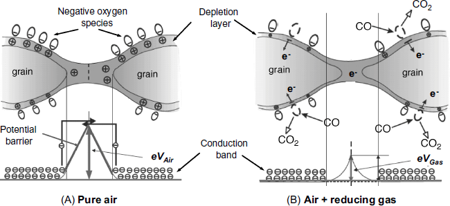
Nonstoichiometric tin oxide (![]() ) behaves as an n-type semiconductor due to oxygen vacancies in the crystal structure. The presence of a vacancy causes two electrons at a tin atom to become free. If tin dioxide is exposed to ambient oxygen, oxygen molecules adsorb at the surface and each oxygen molecule captures one electron, forming adsorbed anionic oxygen species such as
) behaves as an n-type semiconductor due to oxygen vacancies in the crystal structure. The presence of a vacancy causes two electrons at a tin atom to become free. If tin dioxide is exposed to ambient oxygen, oxygen molecules adsorb at the surface and each oxygen molecule captures one electron, forming adsorbed anionic oxygen species such as ![]() ,
, ![]() and
and ![]() (Figure 12.1A). Electron trapping by oxygen depletes the surface of charge carriers, the depletion degree being maximal at the neck between two particles. Hence, electron transfer between adjacent grains is hindered by a potential barrier. The electrical resistance of the sensor (RAir) is determined by this barrier according to the following approximate equation:
(Figure 12.1A). Electron trapping by oxygen depletes the surface of charge carriers, the depletion degree being maximal at the neck between two particles. Hence, electron transfer between adjacent grains is hindered by a potential barrier. The electrical resistance of the sensor (RAir) is determined by this barrier according to the following approximate equation:
(12.1) ![]()
where R0 is a constant, e is the elementary charge, VAir is the barrier height in pure air, kB is the Boltzmann constant, and T is the absolute temperature. Based on this principle, oxygen sensors have been developed using TiO2 or BaTiO3 as sensing materials.
If a reducing gas (for example, carbon monoxide) is present in the air sample, it reacts with adsorbed oxygen species as follows:
(12.2) ![]()
In this way, free electrons are released into the conduction band (Figure 12.1B). As a result, the intergrain energy barrier decreases and the sensor resistance becomes:
(12.3) ![]()
where VGas is the barrier height in the presence of the reducing gas. As VGas < VAir, the resistance becomes smaller under the action of a reducing gas. The material sensitivity to the reducing gas (SMat) can be expressed as:
(12.4) ![]()
Oxidizing gases (such as NO2 or chlorine) can also be detected by certain metal-oxide sensors. In this case, the analyte causes the electron depletion to increase, which results in a greater resistance. More details on the response mechanism of metal-oxide chemiresistors can be found in the literature [3, 4, 7–9].
The relationship between sensor resistance (RS) and the concentration of the analyte gas (c) can be derived from on a theoretical basis [9, 10]. In many cases, the following function represents fairly the sensor response:
(12.5) ![]()
where A and ![]() are empirical parameters and Rref is the resistance measured with a reference gas. Therefore, the response function is linear on a logarithmic scale. This kind of response can extend over a broad concentration range, from several ppb to several thousand ppm. Other empirical correlation functions have also been advanced and are summarized in [3].
are empirical parameters and Rref is the resistance measured with a reference gas. Therefore, the response function is linear on a logarithmic scale. This kind of response can extend over a broad concentration range, from several ppb to several thousand ppm. Other empirical correlation functions have also been advanced and are summarized in [3].
Metal-oxide chemiresistors should by operated at elevated temperatures (200–800 °C), the temperature being regulated by means of an electrical heater included in the sensor layout.
The detection principle of semiconductor oxide gas sensors is based on adsorption and chemical reactions at oxide grain surfaces. Consequently, the operating temperature will affect the sensitivity by determining the rate of chemical reactions. That is why, a circuit for compensation of the temperature variations should be included in the measurement setup.
12.1.3 Response to Humidity
Water vapors adsorb at the surface and cause a certain change in sensor resistance. This property can be advantageously used in resistive humidity sensors for warm gases, the best materials in this respect being perovskite-type mixed oxides containing an alkali-earth metal, such as SrSnO3 and CaTiO3 [11, 12]. The marked response of such materials to water vapors has been ascribed to the strong affinity of alkali-earth ions for water molecules. Very good sensitivity to water vapors has been obtained with Sr0.95 La0.05SnO3, that is, a mixed oxide in which the divalent alkali-earth metal ion is partially substituted by the trivalent lanthanum ion. The above materials are n-type semiconductors and the response to humidity has been assigned to ionized oxygen sites ![]() that promote water dissociation at elevated temperature accompanied by release of a trapped electron from a vacancy
that promote water dissociation at elevated temperature accompanied by release of a trapped electron from a vacancy ![]() :
:
(12.6) ![]()
This mechanism, which involves one electron donation, produces a conductivity modification proportional to ![]() (pw is the partial pressure of water vapor) and has been observed with Sr0.95 La0.05SnO3. Materials with doubly ionized vacancies produce a response proportional to
(pw is the partial pressure of water vapor) and has been observed with Sr0.95 La0.05SnO3. Materials with doubly ionized vacancies produce a response proportional to ![]() , which implies a lower sensitivity.
, which implies a lower sensitivity.
A similar response has been noted with other hydroxyl-containing compounds, such as ethanol.
Certain oxides allow humidity to be gaged by the ionic conduction mechanism (Section). Although many oxides used in such applications are semiconductors, semiconductor properties are not relevant in this case. However, this property can be exploited in the design of multifunctional sensors that respond to humidity at low temperatures and to reducing gases at high temperatures. In the second case, the mechanism presented in Section 12.1.2 is operating.
12.1.4 Sensor Configuration
Initially, gas chemiresistors were fabricated by depositing a thin oxide layer over a ceramic tube as shown schematically in Figure 12.2A. This kind of sensor, which is known as a Taguchi gas sensor, has been commercially available since 1968. The electrical contact to the oxide layer is provided by two metal electrodes placed at the tube ends. Sensor heating is provided by a resistor coil inside the tube. The electrical wiring of the sensor is shown in Figure 12.2B. In order to perform resistance measurements, a constant DC voltage (VS) is applied to the series circuit composed of the sensor and the load resistance RL. According to Ohm's law, the voltage drop across the load resistance (VOUT) is inversely proportional to the sensor resistance. This voltage is the output signal response of the sensor. As can be seen, the measurement principle is very simple and involves only DC circuits.
Figure 12.2 (A) Design of a tin oxide tubular gas sensor; (B) electrical wiring of a resistive gas sensor. VS: sensor voltage; VH: heating voltage; RL: load resistance; VOUT: output voltage.

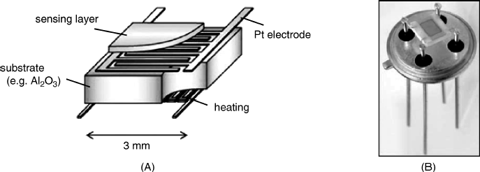
Although the tubular configuration in Figure 12.2 has been in use for long time, it is currently being replaced by a planar configuration, which is more advantageous from the standpoint of fabrication technology. In the planar design (Figure 12.3), the metal oxide layer is deposited over a flat dielectric support and the heater is placed underneath. The electrodes are formed as an interdigitated structure, which makes it possible to use gas-sensitive materials with a very high offset resistivity. Such materials are characterized by a high sensitivity to gas interaction. The planar configuration that allows for miniaturization is compatible with microfabrication technologies such as screen printing and micromachining. Micromachining allows the production of very small sized devices characterized by low power consumption and easy multiplexing [13].
Figure 12.3 (A) Schematics of a planar resistive gas sensor; (B) photograph of a planar gas sensor. Reproduced with permission from [14]. Copyright 2007 Wiley-VCH Verlag GmBH & Co. KGaA.
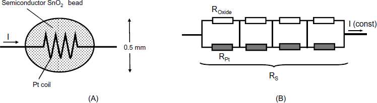
The configurations described above involve two distinct electrical circuits: the heating circuit and the measuring circuit. A simpler configuration that is based on a single electrical circuit is obtained by embedding a platinum coil in a semiconductor oxide bead as shown in Figure 12.4A [15, 16]. This coil functions as a heater but, at the same time, the metal oxide partially short circuits the turns of the coil, as shown in Figure 12.4B. The overall resistance of the device (RS) depends on both the constant coil resistance and the gas-modulated oxide resistance. Such a sensor is called a semistor, a word that is a blend of semiconductor and resistor. The semistor is a very simple device, but since the oxide is shunted by platinum turns, its overall resistance cannot be lower that that of the coil. Hence, small variations of the oxide resistance cannot be detected, which limits the sensor sensitivity. However, this device is useful in applications that are not demanding as far as sensitivity is concerned.
Figure 12.4 The semistor. (A) Configuration; (B) equivalent circuit. RPt represents the resistance of a platinum turn; ROxide is the resistance of the oxide contained between two platinum turns.
12.1.5 Synthesis and Deposition of Metal Oxides
Metal oxides for chemiresistor applications can be obtained by either wet or dry synthesis methods [17].
Sol-gel chemistry was introduced in Section 8.7 and it represents the usual wet synthesis method. Depending on reaction conditions, sol-gel synthesis produces either amorphous or crystalline particles. Their size depends on synthesis parameters such as the precursor concentration or the reaction temperature. Subsequent crosslinking of the sol particles leads to a gel, that is, a porous network impregnated with a liquid phase. To obtain a supported film, the sol is applied to the substrate before gelation. Finally, the solvent is removed from the gel to yield a porous solid, which is subject to calcinations, in order to improve its stability. Sintering of the particles, which occurs during the calcination step, increases the grain connectivity but decreases the specific area. Alternatively, sol-gel synthesis of the oxide can be conducted directly on the support. Nonconventional sol-gel methods have recently been advanced [18].
Dry synthesis offers broad possibilities for rapid production of metal-oxide films of various morphologies, degree of porosity, and thickness. Notably, dry synthesis is compatible with microfabrication technology. A series of dry synthetic methods are based on chemical vapor deposition. This is performed by supplying a gaseous precursor to the high-temperature reaction zone so that the synthesis of the metal oxide takes places directly on the target substrate. In this way, SnO2 can be formed by high-temperature hydrolysis of a SnCl4 solution. An alternative deposition method relies on aerosol synthesis in a flame. In this case, a solution containing the precursor is fed as an aerosol to a flame.
Currently, a broad spectrum of dry synthesis methods are available, each of them providing some particular advantages as far as the control of the grain size, film morphology, and film thickness are concerned [14, 17].
12.1.6 Fabrication of Metal-Oxide Chemiresistors
Planar gas-sensitive layers can be deposited as a thin film between two interdigitated electrodes. Sensors of this type can be manufactured by screen printing on a thin ceramic support.
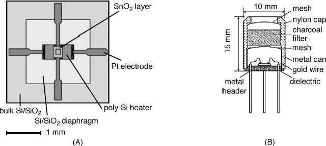
A more advanced fabrication method is based on micromachining that allows production of small-size devices characterized by low power consumption and easy multiplexing [13, 19, 20]. An example of a gas sensor manufactured by micromachining is presented in Figure 12.5. The gas-sensitive layer is formed over a thin dielectric membrane (SiO2 or Si3N4) deposited on a silicon support. The low thermal conductivity of this membrane secures good thermal insulation between the support and the sensitive heated region. In this way, power consumption can be kept very low, typically between 30 and 150 mW and the distance between electrodes can be decreased to the μm range, which permits using interdigitated electrodes integrated with highly resistive sensing materials. In addition, sensor arrays can be easily implemented in this technology.
Figure 12.5 A micromachined gas sensor. (A) Sensor unit; (B) sensor housing. Reproduced with permission from [13]. Copyright 2001 Elsevier.
12.1.7 Selectivity and Sensitivity
A crucial parameter that determines the sensitivity is the size of the oxide grains [21, 22]. The effect of the grain size can be rationalized if the sensitive layer is viewed as a three-dimensional network of grains and necks, each particle being composed of a couple of adherent grains (Figure 12.6). The total resistance of the sensing layer is controlled by the resistance of the grains, necks, and the contact area between particles. In general, a strong increase in the sensor sensitivity is obtained by decreasing the grain size (D) to the nanometer region. The critical parameter in this respect is the Debye length (![]() ), which is the distance over which significant charge separation can occur in the semiconductor. As shown in Figure 12.6A, if the particle size is very large with respect to the Debye length, the depletion layer occupies a very thin region and affects, to a small extent, the current flow along the grain and across the necks. The material resistivity is in this case determined by discontinuities at interparticle zones of contact. If the particle size is just slightly greater that the Debye length (Figure 12.6B), the depletion layer expands over an appreciable fraction of the grain and the conduction is limited to a channel whose thickness is mostly determined by the thickness (LC) of the nondepleted zone within the neck regions. This results in a higher resistivity compared with the previous case. If the particle size is close to twice the Debye length (Figure 12.6C) nearly all the electrons are trapped at the particle surface and the maximum resistivity is obtained. Under these conditions, very small changes in the trapped electron density in response to the gas reaction induce a noticeable variation in the resistance. In general, particle sizes below 100 nm provide a high sensitivity.
), which is the distance over which significant charge separation can occur in the semiconductor. As shown in Figure 12.6A, if the particle size is very large with respect to the Debye length, the depletion layer occupies a very thin region and affects, to a small extent, the current flow along the grain and across the necks. The material resistivity is in this case determined by discontinuities at interparticle zones of contact. If the particle size is just slightly greater that the Debye length (Figure 12.6B), the depletion layer expands over an appreciable fraction of the grain and the conduction is limited to a channel whose thickness is mostly determined by the thickness (LC) of the nondepleted zone within the neck regions. This results in a higher resistivity compared with the previous case. If the particle size is close to twice the Debye length (Figure 12.6C) nearly all the electrons are trapped at the particle surface and the maximum resistivity is obtained. Under these conditions, very small changes in the trapped electron density in response to the gas reaction induce a noticeable variation in the resistance. In general, particle sizes below 100 nm provide a high sensitivity.
Figure 12.6 Effect of grain size on the conductivity of a metal oxide semiconductor in the presence of oxygen. D is the grain size; ![]() is the Debye length. (A) For
is the Debye length. (A) For ![]() the extension of the depletion layer in the neck region is so small that the necks have a minor effect on the resistivity. Resistivity is mostly determined by grain boundaries (bulk conductivity). (B) For D values moderately greater than
the extension of the depletion layer in the neck region is so small that the necks have a minor effect on the resistivity. Resistivity is mostly determined by grain boundaries (bulk conductivity). (B) For D values moderately greater than ![]() , the thickness of the nondepleted zone in the neck region (LC), is very small and determines the resistivity (neck control); (C) for
, the thickness of the nondepleted zone in the neck region (LC), is very small and determines the resistivity (neck control); (C) for ![]() the depletion layer expands over the whole grain thickness. The oxide layer has the lowest conductivity and responds with maximum sensitivity to the analyte gas. Reproduced with permission from [17]. Copyright 2010 Wiley-VCH Verlag GmBH & Co. KGaA.
the depletion layer expands over the whole grain thickness. The oxide layer has the lowest conductivity and responds with maximum sensitivity to the analyte gas. Reproduced with permission from [17]. Copyright 2010 Wiley-VCH Verlag GmBH & Co. KGaA.

The particulate film morphology allows for gas diffusion into the bulk of the film. Nevertheless, compact oxide films can also be used in gas sensing. In this case, the interaction with the gas is limited to the surface of the sensitive layer [9]. Compact layers can be formed as thick or as thin layers. Film thickness is expressed in relative units as the film thickness/Debye length ratio. For a thick film, the film is much thicker than the Debye length and the current flow is limited to the surface conducting channel. Gas interaction modulates the thickness of this channel and hence the film resistivity. Conversely, the thickness of a thin film is comparable with the Debye length and the influence of gas interaction is extended over the whole thickness of the layer.
Sensitivity to a particular gas results from the interplay of a great number of geometrical factors (grain size, porosity, area of intergrain contact and orientation of nanocrystals) and physicochemical parameters (chemical and phase composition, bulk and surface density of oxygen vacancies, and properties of the additives) [23, 24]. Such parameters can be tuned by proper selection of the synthesis method and by post-synthesis treatment of the oxide material.
Generally, metal-oxide resistive gas sensors are not selective and those developed for the determination of reducing gases respond to many compounds of this kind. In order to enhance the response to a particular gas or a class of gases particular additives are added to the semiconductor material. Noble metals that display catalytic properties are common additives that can be applied as a surface layer or can be incorporated through the body of the sensitive layer. Other kinds of additive have also been used.
Selectivity can be enhanced by the addition of a component with which the target analyte will react. Thus, basic oxide additives increase the response to H2S, while acidic oxide additives enhance the sensitivity to NH3.
The effect of noble-metal additives can be rationalized by taking into account the partial charge transfer between adsorbed oxygen and the metal clusters embedded in the oxide [25]. Oxygen adsorption at the metal surface leads to electron depletion in the metal, which raises the work function of the metal and, consequently, leads to an increase in the barrier height and the appearance of an inversion layer at the surface of oxide grains. Maximum resistance is obtained when the density of metal clusters is such as to allow inversion layers in the oxide to overlap. Reducible gases, that can perform partial electron transfer to metal clusters, lower the barrier height and thus enhance the conductivity.
In some instances, a filter that removes interfering gas components provides sufficient selectivity. For example, interference by hydrocarbons in the determination of carbon monoxide can be avoided by using a charcoal filter.
12.1.8 Outlook
Metal-oxide chemiresistors are currently well established devices in industrial and environmental monitoring of atmosphere quality. Industry makes extensive use of such sensors for the detection of hazardous gases, whereas the control of air quality in areas exposed to high traffic or in garages is another important application. Metal-oxide chemiresistors are rugged and inexpensive devices. From the standpoint of functioning characteristics, they are reasonably accurate, reversible, and have a short response time.
Although the gas-recognition selectivity of metal oxides is poor, improvements can be achieved by including various additives, particularly catalytic metals. If high selectivity is needed, one can resort to sensor arrays that allow for accurate determination of the sample components by suitable data-processing methods (see Section 1.7).
The science and technology of metal-oxide chemiresistors is currently at an advanced level and the sound theoretical background of this field provides reliable premises to rational sensor development. Further technological advances are expected from the improvement in the degree of control of the structure and morphology of the oxide layer by microfabrication methods. Much progress in the field of the synthesis of oxidic sensing material is expected from the application of the methods of combinatorial chemistry. Other materials, such as porous silicon, are currently being investigated for application in resistive gas sensors [26, 27].
12.2 Organic-Material-Based Chemiresistors
Easily available carbon-black–polymer composites have demonstrated good performances as resistive gas-sensing materials that respond to organic vapors. Carbon particles provide electric conductivity in such a composite film. Vapor absorption in the polymer matrix causes the composite to swell and, as a result, some of the conductive pathways are broken, which leads to increased resistance.
Thin films of carbon-loaded polymer are well suited for manufacturing inexpensive sensor arrays that can discriminate between various compounds in an organic vapor mixture [28, 29]. Each array unit includes a different polymer type, such as to endow it with particular sensitivity to each component in a mixture. A rational selection of the composite can be made using correlations of sensor response with molecular descriptors [30]. Combinatorial chemistry represent an alternative route to the design of gas polymer composites sensitive to a species of interest [31].
Organic semiconductors, such as phthalocyanines and conducting polymers, are commonly used in chemiresistors [32]. In order to obtain the sensor, organic semiconductors are deposited in the gap between two electrodes over an insulator substrate.
Phthalocyanines are able to form adducts with electron-donor molecules (such as O2, NO and NO2) by electron transfer to an orbital at the central metal ion. This process injects electrons into the conduction band and thus enhances the conductivity of the phthalocyanine film.
Conducting polymers (introduced in Section 5.9) can respond to a wide range of polar or nonpolar gases and vapors depending on various interaction mechanisms [33–35]. Possible interactions between gas molecules and a conducting polymer are represented in Figure 12.7 and are reviewed below in accordance with the site labels in this figure.
Figure 12.7 Possible interactions of a gas molecule with a conducting polymer. X is the analyte; C– is the doping counterion.
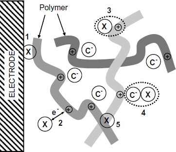
One more possible mechanism is based on polymer swelling under the effect of an organic vapor analyte, which alters the density of counterions and thus modifies the polymer resistivity.
No matter what recognition mechanism operates, the response is generally rapid and reversible at room temperature, in contrast to metal-oxide sensors that should be operated at elevated temperature. The response function is of the Langmuir type. Accordingly, the resistance increases nonlinearly with the analyte concentration at concentrations below the saturation level. The sensor response can be represented as follows [33]:
(12.7) ![]()
where ![]() is the change in resistance in the presence of the analyte (
is the change in resistance in the presence of the analyte (![]() ),
), ![]() is the concentration of the analyte, K is the binding constant,
is the concentration of the analyte, K is the binding constant, ![]() is the resistance in the absence of the analyte, and
is the resistance in the absence of the analyte, and ![]() is the resistance at saturation.
is the resistance at saturation.
Although conducting polymers are also useful in other types of gas sensor, the chemiresistor configuration possesses the great advantages of simplicity and easy fabrication. Selectivity can be readily modulated by post-synthesis treatments that alter of the chemical structure. In addition, these devices are small and function with very low power consumption. Conducting polymers are suitable for applications in sensor arrays for multianalyte determination and artificial nose applications.
12.3 Nanomaterial Applications in Resistive Gas Sensors
Semiconductor metal oxides, that are well-established gas-sensitive materials, have been recently shown to be suitable for applications in gas sensors in the form of nanofibers of about 100 nm diameter. Tin dioxide nanofibers can be obtained by electrospinning of a SnCl4-polyvinyl alcohol solution with subsequent stepwise annealing at 300, 500 and 700 °C. Such nanofibers are woven to obtain a gas-sensing membrane. Due to the small diameter, the depletion layer produced by oxygen extends over a large fraction of the fiber section which gives high sensitivity, short response times, and fast recoveries [36].
Conducting polymers, that display excellent qualities as gas-sensing materials can also be used in the form of nanofibers of 100–500 nm diameter. Either a single fiber or a nanowoven membrane can be employed as the sensing element [36].
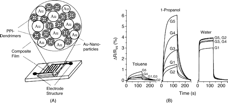
New opportunities in gas sensing arise from the application of metal nanoparticle–organic material composites, such as gold nanoparticles with alkanethiol ligand shells or gold nanoparticle–dendrimer composite films [37]. The response mechanism in this case is based on the absorption of the analyte gas into the organic matrix. Selective recognition can be obtained by introducing specific chemical functionalities into the organic ligand shell. Current flow through nanoparticle–organic composites proceeds by electron hopping between adjacent particles. As a result of analyte interaction with the organic matrix, the interparticle spacing is altered, which can affect either the interparticle energy barrier or the transmission probability for electron tunneling through the barrier. A change in the work function of the metal in response to gas adsorption is another possible mechanism that may operate in the case of gases that display Lewis acid or base properties. By partial charge transfer between such an analyte and the nanoparticle, the Fermi level of the metal is altered. The resulting modification of the metal work function brings about a change in the potential barrier to the electron hopping between particles.
Details of the structure of a resistive gas sensor based on gold nanoparticles–dendrimer composite material are shown in Figure 12.8A. This dendrimer consists of poly(propyleneimine) and the sensing layer is deposited on a couple of interdigitated electrodes. Sensitivity to various analytes (toluene, propanol, and water vapor) depends to a large extent on dendrimer generation, as demonstrated in Figure 12.8B. Clearly, the best sensitivity to 1-propanol is obtained with the generation 5 dendrimer, whereas the sensitivity to toluene is relatively low, although it increases with increasing dendrimer generation. It was assumed in this work that the effect of the dendrimer generation is determined by the capture of organic molecules within the interior structure of dendrimers. The response to water vapor is affected to a very small extent by the dendrimer generation, which suggests that water vapor interacts with primary amino groups at the surface of the dendrimers. Therefore, the sensitivity of this kind of sensor can be tuned by adjusting the structure of the organic component in the composite material.
Figure 12.8 A chemiresistor with a sensitive layer composed of gold nanoparticles–dendrimer composite material. (A) Structure of the sensing layer and the sensor layout; (B) Sensor response to several vapors as a function of dendrimer generation (G). PPI stands for poly(propyleneimine). Reproduced with permission from [38]. Copyright 2003 Elsevier.
Metal nanoparticle–organic matrix composites are very versatile sensing materials in gas and vapor sensors. The main limitation of such materials arises from their relatively poor thermal stability.
Single-walled carbon nanotubes represent another kind of advanced material that is suitable for gas detection [39]. By charge-transfer interaction with electron-donor or -acceptor gases, the density of charge carrier in the nanotube is altered and, consequently, the conductivity is modified. For example, ammonia (an electron donor) lessens the conductivity of p-type semiconducting nanotubes, while NO2 (an electron acceptor) causes an increase in conductivity.
Adsorption of such gases to the nanotube surface is irreversible, which causes the nanotube device to act like a dosimeter which reports on the levels of exposure to the analyte-gas. Sensor regeneration can be performed by exposing the device to heat or ultraviolet light.
Carbon-nanotube gas sensors can be produced by depositing a network of nanotubes between two interdigitated electrodes. Some degree of selectivity can be imparted by special sorbent polymers coated as thin films (<100 nm) over the nanotube layer. Resistive carbon-nanotube gas sensors show promising perspectives for applications in sensor arrays.
12.4 Resistive Gas Sensor Arrays
Due to the simple fabrication technology, resistive gas sensors are very attractive for application in array format. A sensor array compensates for the poor selectivity of sensing materials and can be operated as an electronic nose device.
A gas sensor array can be obtained simply by assembling a number of discrete sensors based on different sensing materials. However, the size of the array increases with the number of individual sensors and, in the case of high-temperature-operated sensors, the power consumption also increases.
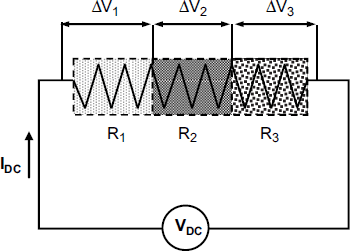
A more versatile alternative is based on an array of different sensing materials deposited over a common substrate, as shown in Figure 12.9. The sequence of sensing layers is crossed by a constant current (![]() ) supplied by a common voltage source. In order to asses the resistance of each sensing layer, the voltage drop (
) supplied by a common voltage source. In order to asses the resistance of each sensing layer, the voltage drop (![]() ) over each on them is measured individually and the particular resistance is obtained as
) over each on them is measured individually and the particular resistance is obtained as ![]() .
.
Figure 12.9 Multipoint probe measurement in a resistive sensor array. Each section of the device is coated with a layer with particular responsive characteristics. R1, R2, and R3 indicates the resistance of each layer. Probe contacts are formed at the boundary of each section to measure the pertinent resistance.
A sequence of different sensing layers as that shown in Figure 12.9 can be produced by depositing first the same type of sensing material (e.g., a metal oxide) over the whole sensing area. A varying degree of selectivity is imparted then to each section by individual modification with suitable additives, such as platinum metals. A similar structure can be built up using various carbon-black–polymer composites or organic semiconductors.
Advanced design of gas sensor arrays is based on integration of a number of discrete sensors produced by microfabrication technology, such as complementary metal-oxide-semiconductor (CMOS) technology that is widely used in manufacturing integrated electronic microcircuits. As demonstrated in Figure 12.10A, each individual sensor can be formed on a platform suspended over a cavity etched in the silicon chip and supported by four legs. This arrangement minimizes the heat transfer to the ambient atmosphere. Details of this sensor structure are illustrated by the cross section in Figure 12.10B. A Pt/Ti bilayer pattern deposited over a SiO2 insulating layer (TO) functions as both heater and resistive thermometer. Next, the SiO2-Si3N4-SiO2 multilayer (ML) provides insulation of the sensing layer from the Pt/Ti electrodes. These electrodes are coated with a passivation SiO2 film (PO). Finally, the SnO2 sensing layer is deposited by oxygen-radical-assisted electron beam evaporation of a metal target. The oxide formed in this way proved to respond with high sensitivity to ethanol vapors with negligible interference of other gases such as carbon monoxide, hydrogen, methane and isobutene vapors.
Figure 12.10 Structure of a resistive gas sensor fabricated by micromachining technology. TO: SiO2 insulating layer; ML: SiO2-Si3N4-SiO2 multilayer insulator; PO: passivation SiO2 film. Reproduced with permission from [40]. Copyright 2001 Elsevier.
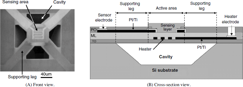
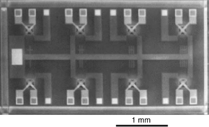
Figure 12.11 displays a magnified view of a sensor array composed of eight distinct sensors similar to that shown in Figure 12.10. This array is characterized by low power consumption and can be produced by standard microelectronics technology, which allows for a high degree of integration.
Figure 12.11 Topography of a micromachined 2 × 4 resistive gas sensor array produced by micromachining. Reproduced with permission from [40]. Copyright 2001 Elsevier.
12.5 Summary
Gas and vapor determination is a current analytical problem in various areas such as industry and in air-quality monitoring, which prompted the development gas sensors, particularly for the detection of flammable or toxic gases and vapors. There are various types of gas sensor that can, in principle, fulfill such functions. Among them, resistive gas sensors based on semiconductor sensing materials occupy an important position. Well-established sensors of this type make use of metal-oxide semiconductors and are currently produced on a large-scale basis.
What is important with regard to metal-oxide resistive gas sensors is the simple constructive principle and facile measurement procedure, combined with excellent ruggedness and reliability.
Besides metal oxides, organic semiconductors have emerged as a new class of gas sensing material with applications in resistive gas sensors. Organic semiconductors provide a large number of possibilities of adjusting the sensing parameters either directly, by synthesis, or by postsynthesis modification. As organic semiconductors can interact with gases and vapors by a multitude of different mechanisms, their field application is potentially very broad. In addition, organic-semiconductor-based sensor can be operated at ambient temperature, which has the advantage of very low power consumption.
Nanomaterial application in the field of resistive gas sensors represents another line of development. Actually, well-established metal-oxide semiconductors function best when the material is structured at the nanoscale. Distinct nanoparticles, such as carbon nanotubes and metal nanoparticles are newcomers in this field, but have aroused much interest and a number of applications have already been developed.
A new trend in the fabrication of gas sensors is based on printing on flexible, plastic foils [41]. This technology is suitable for manufacturing both resistive and capacitive sensors and allows integration of multiple sensors into sensor arrays. Microelectronic circuits can also be integrated with the sensor for signal processing and interfacing
Typically, resistive gas sensors are characterized by moderate selectivity. This is not a major drawback in gas-leakage monitoring in industry, where no complex mixtures of gases have to be tested. As usually, the selectivity problem can be conveniently addressed by resorting to arrays of crossreactive sensors. In this respect, resistive gas sensors have the advantage of simple fabrication technology and resistive gas sensor arrays are already well established in the development of electronic nose devices.
1. Dinesh, K. and Gupta, S.K. (eds) (2007) Science and Technology of Chemiresistor Gas Sensors, Nova, New York.
2. Hoffheins, B. (1996) Solid state, resistive gas sensors, in Handbook of Chemical and Biological Sensors (eds R.F. Taylor and J.S. Schultz), Institute of Physics Publishing, Bristol, pp. 371–397.
3. Bârsan, N., Schweizer-Berberich, M., and Göpel, W. (1999) Fundamental and practical aspects in the design of nanoscaled SnO2 gas sensors: a status report. Fresenius J. Anal. Chem., 365, 287–304.
4. Bârsan, N., Koziej, D., and Weimar, U. (2007) Metal oxide-based gas sensor research: How to? Sens. Actuators B-Chem., 121, 18–35.
5. Korotcenkov, G. (2007) Metal oxides for solid-state gas sensors: What determines our choice? Mater. Sci. Eng. B-Solid State Mater. Adv. Technol., 139, 1–23.
6. Licznerski, B.W. (2004) Thick-film gas microsensors based on tin dioxide. Bull. Polish Acad. Sci.-Technical Sci., 52, 37–42.
7. Kohl, D. (2001) Function and applications of gas sensors. J. Phys. D-Appl. Phys., 34, R125–R149.
8. Park, C.O. and Akbar, S.A. (2003) Ceramics for chemical sensing. J. Mater. Sci., 38, 4611–4637.
9. Bârsan, N. and Weimar, U. (2001) Conduction model of metal oxide gas sensors. J. Electroceram., 7, 143–167.
10. Williams, D.E. (1999) Semiconducting oxides as gas-sensitive resistors. Sens. Actuators B-Chem., 57, 1–16.
11. Seiyama, T., Yamazoe, N., and Arai, H. (1983) Ceramic humidity sensors. Sens. Actuators, 4, 85–96.
12. Traversa, E. (1995) Ceramic sensors for humidity detection – the state-of-the-art and future-developments. Sens. Actuators B-Chem., 23, 135–156.
13. Simon, T., Bârsan, N., Bauer, M. et al. (2001) Micromachined metal oxide gas sensors: opportunities to improve sensor performance. Sens. Actuators B-Chem., 73, 1–26.
14. Tiemann, M. (2007) Porous metal oxides as gas sensors. Chem.-Eur. J., 13, 8376–8388.
15. Williams, G. and Coles, G.S.V. (1999) The semistor: A new concept in selective methane detection. Sens. Actuators B-Chem., 57, 108–114.
16. Korotcenkov, G. (2007) Practical aspects in design of one-electrode semiconductor gas sensors: Status report. Sens. Actuators B-Chem., 121, 664–678.
17. Tricoli, A., Righettoni, M., and Teleki, A. (2010) Semiconductor gas sensors: Dry synthesis and application. Angew. Chem.-Int. Edit., 49, 7632–7659.
18. Neri, G. (2010) Non-conventional sol-gel routes to nanosized metal oxides for gas sensing: From materials to applications. Sci. Adv. Mater., 2, 3–15.
19. Spannhake, J., Helwig, A., Schulz, O. et al. (2009) Micro-fabrication of gas sensors, in Solid State Gas Sensing (eds E. Comini, G. Faglia, and G. Sberveglieri), Springer Science+Business Media, LLC, Boston, MA, pp. 1–46.
20. Yamazoe, N. (2005) Toward innovations of gas sensor technology. Sens. Actuators B-Chem., 108, 2–14.
21. Rothschild, A. and Komem, Y. (2004) The effect of grain size on the sensitivity of nanocrystalline metal-oxide gas sensors. J. Appl. Phys., 95, 6374–6380.
22. Korotcenkov, G., Han, S.D., Cho, B.K. et al. (2009) Grain size effects in sensor response of nanostructured SnO2-and In2O3-based conductometric thin film gas sensor. Crit. Rev. Solid State Mater. Sci., 34, 1–17.
23. Korotcenkov, G. (2005) Gas response control through structural and chemical modification of metal oxide films: state of the art and approaches. Sens. Actuators B-Chem., 107, 209–232.
24. Korotcenkov, G. (2008) The role of morphology and crystallographic structure of metal oxides in response of conductometric-type gas sensors. Mater. Sci. Eng. R-Rep., 61, 1–39.
25. Licznerski, B.W., Nitsch, K., Teterycz, H. et al. (2001) The influence of Rh surface doping on anomalous properties of thick-film SnO2 gas sensors. Sens. Actuators B-Chem., 79, 157–162.
26. Ozdemir, S. and Gole, J.L. (2007) The potential of porous silicon gas sensors. Curr. Opin. Solid State Mater. Sci., 11, 92–100.
27. Korotcenkov, G. and Cho, B.K. (2010) Porous semiconductors: Advanced material for gas sensor applications. Crit. Rev. Solid State Mater. Sci., 35, 1–37.
28. Lonergan, M.C., Severin, E.J., Doleman, B.J. et al. (1996) Array-based vapor sensing using chemically sensitive, carbon black-polymer resistors. Chem. Mater., 8, 2298–2312.
29. Patel, S.V., Jenkins, M.W., Hughes, R.C. et al. (2000) Differentiation of chemical components in a binary solvent vapor mixture using carbon/polymer composite-based chemiresistors. Anal. Chem., 72, 1532–1542.
30. Shevade, A.V., Homer, M.L., Taylor, C.J. et al. (2006) Correlating polymer-carbon composite sensor response with molecular descriptors. J. Electrochem. Soc., 153, H209–H216.
31. Potyrailo, R.A. (2006) Polymeric sensor materials: Toward an alliance of combinatorial and rational design tools? Angew. Chem. Int. Edit., 45, 702–723.
32. Sadaoka, Y. (1992) Organic semiconductor gas sensors, in Gas Sensors: Principles, Operation and Developments (ed. G. Sberveglieri), Kluwer, Dordrecht, pp. 187–218.
33. Gardner, J.W. and Bartlett, P.N. (1999) Electronic Noses: Principles and Applications, Oxford University Press, Oxford.
34. Lange, U., Roznyatouskaya, N.V., and Mirsky, V.M. (2008) Conducting polymers in chemical sensors and arrays. Analyt. Chim. Acta, 614, 1–26.
35. Bai, H. and Shi, G.Q. (2007) Gas sensors based on conducting polymers. Sensors, 7, 267–307.
36. Ding, B., Wang, M.R., Yu, J.Y. et al. (2009) Gas sensors based on electrospun nanofibers. Sensors, 9, 1609–1624.
37. Franke, M.E., Koplin, T.J., and Simon, U. (2006) Metal and metal oxide nanoparticles in chemiresistors: Does the nanoscale matter? Small, 2, 36–50.
38. Krasteva, N., Guse, B., Besnard, I. et al. (2003) Gold nanoparticle/PPI-dendrimer based chemiresistors Vapor-sensing properties as a function of the dendrimer size. Sens. Actuators B-Chem., 92, 137–143.
39. Snow, E.S., Perkins, F.K., and Robinson, J.A. (2006) Chemical vapor detection using single-walled carbon nanotubes. Chem. Soc. Rev., 35, 790–798.
40. Mo, Y.W., Okawa, Y., Tajima, M. et al. (2001) Micro-machined gas sensor array based on metal film micro-heater. Sens. Actuators B-Chem., 79, 175–181.
41. Briand, D., Oprea, A., Courbat, J. et al. (2011) Making environmental sensors on plastic foil. Mater. Today, 14, 416–423.