
11
COMPENSATORS
11.1 Introduction
The ultimate goal of examining the time domain analysis, frequency domain analysis and stability of a system in the previous chapters is to design a control system. The specific tasks for a system or requirements of a system can be achieved by a proper design of control systems. The performance specifications of a system generally relate to accuracy, stability and response time and these also vary based on the domain by which the system is to be designed. When the performance specifications of a system are given in time domain, the design can be carried out using any time-domain techniques and also if the performance specifications of a system are given in frequency domain, then the design can be carried out using any frequency domain techniques.
The general step followed in designing a control system is adjusting the gain of the system to meet its requirements. In practical situations, adjustment of gain may lead a system to unstable region or it may not be sufficient to meet the desired specifications. In such situations, additional devices or components can be added to the system to meet the specifications or to make the system stable. The additional devices or components that are added to a system are called compensators. The procedure for designing the compensators of a single-input single-output linear time invariant control system is discussed in this chapter. The steps to be followed in designing a control system are:
- Determine how the system functions and what the system has to do.
- Determine the controller or compensator that can be more suitable for the given system.
- Determine the parameters or constants present in the controller or compensator transfer function that has been chosen in the previous step.
11.2 Compensators
The compensator circuits basically introduce a pole and/or zero to the existing system to meet the desired specifications. The compensators may be designed using electrical, mechanical, pneumatic or any other components. The basic idea of determining the transfer function of the compensator is to suitably place the dominant closed-loop poles of a system. Compensated systems can be classified into six categories based on the location of compensators in the system as follows:
- Series or cascade compensation
- Feedback or parallel compensation
- Load or series-parallel compensation
- State feedback compensation
- Forward compensation with series compensation
- Feed-forward compensation
11.2.1 Series or Cascade Compensation
In this type of compensated system, the compensator is included in the feed-forward path of the system as shown in Fig. 11.1(a).

Fig. 11.1(a) ∣ Series or cascade compensation
The addition of compensator in the feed-forward path adjusts the gain of a system which reduces the response time and peak overshoot of the system. In addition, the stability of the system gets reduced.
11.2.2 Feedback or Parallel Compensation
In this type of compensated system, the compensator is included in the feedback path of a system as shown in Fig. 11.1(b).

Fig. 11.1(b) ∣ Parallel or feedback compensation
The addition of compensator in the feedback path increases the response time of the system that makes it accurate and more stable.
11.2.3 Load or Series-Parallel Compensation
The combination of both series and parallel compensation shown in Fig. 11.1(c) is known as load or series - parallel compensation.

Fig. 11.1(c) ∣ Series-parallel or load compensation
11.2.4 State Feedback Compensation
In this type of compensation, the control signal in the form of state variable is fed back as a control signal through the constant real gain as shown in Fig. 11.1(d).

Fig. 11.1(d) ∣ State feedback compensation
The implementation of the state feedback compensation is costly and impractical for higher order systems.
11.2.5 Forward Compensation with Series Compensation
When a simple closed-loop system is in series with the feed-forward controller, ![]() , the resultant compensation is the forward compensation with series compensation that is shown in Fig. 11.1(e).
, the resultant compensation is the forward compensation with series compensation that is shown in Fig. 11.1(e).

Fig. 11.1(e) ∣ Forward compensation with series compensation
11.2.6 Feed-forward Compensation
When the feed-forward controller ![]() is placed in parallel with the forward path of a simple closed-loop system, the resultant compensation is the feed-forward compensation that is shown in Fig. 11.1(f).
is placed in parallel with the forward path of a simple closed-loop system, the resultant compensation is the feed-forward compensation that is shown in Fig. 11.1(f).

Fig. 11.1(f) ∣ Feed-forward compensation
The compensated systems shown in Figs. 11.1(a), 11.1(b) and 11.1(d) have one degree of freedom which intimates that the system has single controller. The disadvantage of one degree of freedom controller is that the performance criteria realized using these compensation techniques are limited.
In simple words, the compensators introduce additional poles/zeros to an existing system so that the desired specification is achieved.
11.2.7 Effects of Addition of Poles
The following are the effects of addition of poles to an existing system:
- The root locus of a compensated system will be shifted towards the right-hand side of the s-plane.
- Stability of a system gets lowered.
- Settling time of a system increases.
- Accuracy of a system is improved by the reduction of steady-state error.
11.2.8 Effects of Addition of Zeros
The following are the effects of addition of zeros to an existing system:
- The root locus of a compensated system will be shifted towards the left-hand side of the s-plane.
- Stability of a system gets increased.
- Settling time of a system decreases.
- Accuracy of a system is lowered as steady-state error of the system increases.
In this chapter, three types of compensators used in the electrical systems are discussed. They are:
- Lag compensators
- Lead compensators
- Lag–lead compensators
11.2.9 Choice of Compensators
The choice of compensators from the different categories discussed in the previous sections is based on the following factors:
- Nature of signal to the system
- Available components
- Experience of the designer
- Cost
- Power levels at different points and so on
11.3 Lag Compensator
The lag compensator is one that has a simple pole and a simple zero in the left half of the s-plane with the pole nearer to the origin. The term lag in the lag compensator means that the output voltage lags the input voltage and the phase angle of the denominator of the transfer function is greater than that of numerator. The general transfer function of the lag compensator is given by
 ,
, ![]() (11.1)
(11.1)
where ![]() are the constants and
are the constants and ![]() .
.
The pole-zero configuration of the lag compensator is shown in Fig. 11.2.

Fig. 11.2 ∣ Pole-zero configuration of Gla(s)
The corner frequencies present in the lag compensator, whose transfer function is given by Eqn. (11.1) are at ![]() and
and ![]() . The Bode plot and polar plot of the lag compensator are shown in Figs. 11.3(a) and 11.3(b) respectively.
. The Bode plot and polar plot of the lag compensator are shown in Figs. 11.3(a) and 11.3(b) respectively.


Fig. 11.3 ∣ Plots of lag compensator
The Bode plot shown in Fig. 11.3(a) is plotted with ![]() and
and ![]() . It is inferred that (i) magnitude of lag compensator is high at low frequencies and (ii) magnitude of lag compensator is zero at high frequencies. Hence, from the above conclusions, it is clear that the lag compensator behaves like a low-pass filter. The value of
. It is inferred that (i) magnitude of lag compensator is high at low frequencies and (ii) magnitude of lag compensator is zero at high frequencies. Hence, from the above conclusions, it is clear that the lag compensator behaves like a low-pass filter. The value of ![]() is chosen between 3 and 10. The magnitude plot and phase plot of the compensator with different values of
is chosen between 3 and 10. The magnitude plot and phase plot of the compensator with different values of ![]() are shown in Figs. 11.4(a) and 11.4(b) respectively.
are shown in Figs. 11.4(a) and 11.4(b) respectively.


Fig. 11.4 ∣ Bode plot for different values of ![]() (a) magnitude plot and (b) phase plot
(a) magnitude plot and (b) phase plot
11.3.1 Determination of Maximum Phase Angle Φm
The modified transfer function of the lag compensator is
![]() (11.2)
(11.2)
The magnitude and phase angle of the lag compensator are
 (11.3)
and ![]() (11.4)
(11.4)
The maximum phase angle ![]() occurs at
occurs at

Differentiating Eqn. (11.4) with respect to ω, we obtain
![]()
![]()
![]()
Solving the above equation, we obtain
 (11.5)
Substituting the above equation in Eqn. (11.4), we obtain
![]() (11.6)
(11.6)
Thus, Eqn. (11.5) gives the frequency at which the phase angle of the system is maximum and Eqn. (11.6) gives the maximum phase angle of the lag compensator.
11.3.2 Electrical Representation of the Lag Compensator
A simple lag compensator using resistor and capacitor is shown in Fig. 11.5.
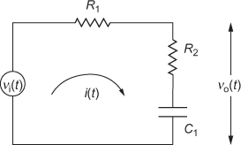
Fig. 11.5 ∣ A simple lag compensator
Applying Kirchoff's voltage law to the above circuit, we obtain
![]() (11.7)
(11.7)
and ![]() (11.8)
(11.8)
Taking Laplace transform on both sides of Eqs. (11.7) and (11.8), we obtain
 (11.9)
and  (11.10)
Substituting ![]() from Eqs. (11.10) to (11.9), we obtain
from Eqs. (11.10) to (11.9), we obtain

Therefore, the transfer function of the above circuit is

Rearranging the above equation, we obtain
 (11.11)
Comparing Eqn. (11.1) and Eqn. (11.11), we obtain
![]() ,
, ![]() and
and ![]() .
.
11.3.3 Effects of Lag Compensator
The following are the effects of adding lag compensator to a given system are:
- The lag compensator attenuates the high-frequency noise signals in the control loop.
- It increases the steady-state error constants of a system.
- Gain crossover frequency of a compensated system gets lowered.
- Bandwidth of the compensated system decreases.
- Maximum peak overshoot, rise time and settling time of the system increases.
- The system becomes more sensitive to the parameter variations.
- As it acts like a proportional integral controller, it makes the system less stable.
- Transient response of the compensated system becomes slower.
11.3.4 Design of Lag Compensator
The objective of designing the lag compensator is to determine the values of ![]() and
and ![]() for an uncompensated system
for an uncompensated system ![]() based on the desired system requirements. The design of lag compensator is based on the frequency domain specifications or time-domain specifications. The Bode plot is used for designing the lag compensator based on the frequency domain specifications, whereas the root locus technique is used for designing the lag compensator based on the time-domain specifications. Once the values of
based on the desired system requirements. The design of lag compensator is based on the frequency domain specifications or time-domain specifications. The Bode plot is used for designing the lag compensator based on the frequency domain specifications, whereas the root locus technique is used for designing the lag compensator based on the time-domain specifications. Once the values of ![]() and
and ![]() are determined, the transfer function of the lag compensator
are determined, the transfer function of the lag compensator ![]() can be obtained. The transfer function of the compensated system is
can be obtained. The transfer function of the compensated system is ![]() . If the Bode plot or root locus technique is plotted for the compensated system, it will satisfy the desired system requirements.
. If the Bode plot or root locus technique is plotted for the compensated system, it will satisfy the desired system requirements.
11.3.5 Design of Lag Compensator Using Bode Plot
Consider the open-loop transfer function of the uncompensated system ![]() . The objective is to design a lag compensator
. The objective is to design a lag compensator ![]() for
for ![]() so that the compensated system
so that the compensated system ![]() will satisfy the desired system requirements. The steps for determining the transfer function of the compensated system
will satisfy the desired system requirements. The steps for determining the transfer function of the compensated system ![]() using Bode plot are explained below:
using Bode plot are explained below:
Step 1:If the open-loop transfer function of the system ![]() has a variable
has a variable ![]() , then
, then ![]() or
or ![]() .
.
Step 2:Depending on the input and TYPE of the system, the variable ![]() present in the transfer function of the uncompensated system
present in the transfer function of the uncompensated system ![]() is determined based on either the steady-state error or the static error constant of the system.
is determined based on either the steady-state error or the static error constant of the system.
The static error constants of the system are:
Position error constant, ![]()
Velocity error constant, ![]()
Acceleration error constant, ![]()
The relation between the steady-state error and static error constant based on the TYPE of the system and input applied to the system can be referred to Table 5.5 of Chapter 5.
Step 3:Construct the Bode plot for ![]() with gain
with gain ![]() obtained in the previous step and determine the frequency domain specifications of the system (i.e., phase margin, gain margin, phase crossover frequency and gain crossover frequency).
obtained in the previous step and determine the frequency domain specifications of the system (i.e., phase margin, gain margin, phase crossover frequency and gain crossover frequency).
Step 4:Let the desired phase margin of the system be ![]() . With a tolerance
. With a tolerance ![]() , determine
, determine ![]() as
as
![]()
where ![]() to
to ![]() .
.
Step 5:Determine the new gain crossover frequency of the system for the phase margin ![]() . Let it be
. Let it be ![]() .
.
Step 6:Determine the magnitude A of the system in dB from the magnitude plot corresponding to ![]() .
.
Step 7:As the magnitude of system at the gain crossover frequency must be zero, the Bode plot must be either increased or decreased by ![]() dB.
dB.
Step 8:The value of ![]() in the transfer function of the lag compensator will be determined as
in the transfer function of the lag compensator will be determined as
![]()
Here ![]() is when the magnitude plot is to be increased and
is when the magnitude plot is to be increased and ![]() is when the magnitude plot is to be decreased.
is when the magnitude plot is to be decreased.
Step 9:The value of ![]() in the transfer function of the lag compensator will be determined by using the equation,
in the transfer function of the lag compensator will be determined by using the equation,  .
.
Step 10: Thus, the transfer function of the lag compensator will be determined as

Step 11: The transfer function of the compensated system will be ![]() . If the Bode plot for the compensated system is drawn, it will satisfy the desired system requirements.
. If the Bode plot for the compensated system is drawn, it will satisfy the desired system requirements.
The flow chart for determining the parameters present in the transfer function of the lag compensator using Bode plot is shown in Fig. 11.6.

Fig. 11.6 ∣ Flow chart for designing the lag compensator using Bode plot
Example 11.1 Consider a unity feedback uncompensated system with the open-loop transfer function as ![]() . Design a lag compensator for the system such that the compensated system has static velocity error constant Kv = 20 sec−1, phase margin
. Design a lag compensator for the system such that the compensated system has static velocity error constant Kv = 20 sec−1, phase margin ![]() and gain margin
and gain margin ![]() .
.
Solution
- Let
 and desired phase margin
  .
. - The value of
 is determined by using
  as
as

Solving the above equation, we obtain
 .
. - The Bode plot for
 H(s) = 1 is drawn.
- Given

- Substituting
 and
and  in the above equation, we obtain

- The corner frequency existing in the given system is
 rad/sec
To sketch the magnitude plot:
- The changes in slope at different corner frequencies are given in Table E11.1(a).
Table E11.1(a) ∣ Determination of change in slope at different corner frequencies

- Assume the lower frequency as ωl = 0.1 rad/sec and higher frequency as
 = 20 rad/sec.
 - The values of gain at different frequencies are determined and given in Table E11.1(b).
Table E11.1(b) ∣ Gain at different frequencies
- The magnitude plot of the given system is plotted using Table E11.1(b) and is shown in Fig. E11.1.
To sketch the phase plot:
- The phase angle of the given loop transfer function as a function of frequency is obtained as

- The phase angle at different frequencies is obtained using the above equation and the values are tabulated as shown in Table E11.1(c).
Table E11.1(c) ∣ Phase angle of a system for different frequencies

- The phase plot of a given system is plotted with the help of Table E11.1(c) and is shown in Fig. E11.1(a).

Fig. E11.1(a)
- The frequency domain specifications of the given system are:
Gain crossover frequency,
 rad/sec.
Phase crossover frequency,
 rad/sec.
Gain margin,
 dB
dBPhase margin,

It can be noted that the uncompensated system is stable, but the phase margin of the system is less than the desired phase margin which is
 .
.
- Given
- Let
 .
. - The new gain crossover frequency for
 is
is  = 0.92 rad/sec.
 - The magnitude of the system corresponding to
 is A = 27 dB.
 - The magnitude plot of the uncompensated system is decreased by 27 dB so that the gain at
 is zero dB.
 - The value of
 in the lag compensator will be determined as

i. e.,

- The value of
 in the transfer function of the lag compensator is determined as

i. e.,

- Thus, the transfer function of the lag compensator is

- Thus, the transfer function of the compensated system is

11.3.6 Design of Lag Compensator Using Root Locus Technique
When a system is desired to meet the static error constant alongwith other time-domain specifications such as peak overshoot, rise time, settling time, damping ratio of the system and undamped natural frequency of oscillation, then lag compensator will be designed using root locus technique. The step-by-step procedure for designing the lag compensator using root locus technique is discussed below:
Step 1:The root locus of an uncompensated system with the loop transfer function ![]() is constructed.
is constructed.
Step 2:Determine ![]() using
using ![]() .
.
Step 3:Draw a line from origin with an angle ![]() from the negative real axis and determine the point at which it cuts the root locus of the uncompensated system. Let that point be the dominant pole of the closed-loop system
from the negative real axis and determine the point at which it cuts the root locus of the uncompensated system. Let that point be the dominant pole of the closed-loop system ![]() .
.
Step 4:If the uncompensated system has a gain ![]() , the gain
, the gain ![]() is determined by using the formula
is determined by using the formula ![]() , or else, we can proceed to the next step.
, or else, we can proceed to the next step.
Step 5:The static error constant of the uncompensated system is determined by
Position error constant, ![]()
Velocity error constant, ![]()
Acceleration error constant, ![]()
Let the static error constant determined for the system be ![]() .
.
Step 6:Determine the factor by which the static error constant is to be increased is determined by using
![]()
Step 7:Select the zero and pole of the lag compensator which lie very close to the origin such that the pole lies right to zero of the compensator. Let z and p be the zero and pole of the compensator. The pole and zero are chosen such that z = 10p.
Step 8:The transfer function of the lag compensator is obtained as ![]() .
.
Step 9:The transfer function of the compensated system is obtained as ![]() .
.
Step 10:The root locus of the compensated system is drawn and with the help of the damping ratio ![]() , the dominant pole of the compensated system is determined. The new dominant pole obtained is
, the dominant pole of the compensated system is determined. The new dominant pole obtained is ![]() .
.
Step 11:The constant ![]() is determined by using
is determined by using ![]() .
.
Step 12:If the static error constant of the compensated system is determined, it will satisfy the desired specifications.
Step 13:If the static error constant does not satisfy the desired specifications, then alternative values of z and p are chosen and step 7–12 will be continued; otherwise, we can stop the procedure.
Thus, the transfer function of the lag compensator using root locus technique is determined.
The flow chart for designing the lag compensator using root locus technique is shown in Fig. 11.7.

Fig. 11.7 ∣ Flow chart for designing the lag compensator
Example 11. 2: Consider a unity feedback uncompensated system with the open-loop transfer function as ![]() . Design a lag compensator for the system such that the compensated system has static velocity error constant
. Design a lag compensator for the system such that the compensated system has static velocity error constant ![]() , damping ratio
, damping ratio ![]() and settling time
and settling time ![]() sec.
sec.
Solution:
- The root locus for an uncompensated system is drawn.
- For the given system
 , the poles are at 0, –1 and –4 i.e.,
  and zeros does not exist i.e.,
  .
. - Since
 , the number of branches of the root loci for the given system is
  .
. - The details of the asymptotes are:
- Number of asymptotes for the given system
 .
. - Angles of asymptotes
 for
for 
Therefore,

- Centroid

- Number of asymptotes for the given system
- As all the poles and zeros are real values, there is no necessity to calculate the angle of departure and angle of arrival.
- To determine the number of branches existing on the real axis.
If we look from the pole p = –1, the total number of poles and zeros existing on the right of –1 is one (odd number). Therefore, a branch of root loci exists between –1 and 0.
Similarly, if we look from the point at
 , the total number of poles and zero existing on the right of the point is three (odd number). Therefore, a branch of root loci exists between
  and –4.
Hence, two branches of root loci exist on the real axis for the given system.
- The breakaway/break-in points for the given system are determined by
 (1)
(1)For the given system, the characteristic equation is
 (2)
(2)i.e.,

Therefore,

Differentiating the above equation with respect to
 and using Eqn. (1), we obtain

Solving for s, we obtain

(i) For
 , K is 0.8794. Since
  is positive, the point
  is a breakaway point. (ii) For
  , K is –6.064. Since
  is negative, the point
  is not a breakaway point.
Hence, only one breakaway point exists for the given system.
- The point at which the branch of root loci intersects the imaginary axis is determined as follows:
Using Eqn. (2), the characteristic equation for the given system is

i.e.,
 (3)
(3)Routh array for the above equation is

To determine the point at which the root loci crosses the imaginary axis, the first element in the third row must be zero i.e.,
 . Therefore,
  .
.As K is a positive real value, the root locus crosses the imaginary axis and the point at which it crosses imaginary axis is obtained by substituting K in Eqn. (3) and solving for s.
The solutions for the cubic equation
 are
are  .
.Hence, the point in the imaginary axis where the root loci crosses is
 .
.The complete root locus for the system is shown in Fig. E11.2.

Fig. E11.2
- For the given system
- Using
 and settling time
  , the dominant closed-loop poles are
 (since
  ).
). - The gain K at dominant closed-loop poles is obtained using the magnitude condition,


i. e.,
 .
.Therefore, the transfer function of the compensated system is
 .
. - The static error constant for the uncompensated system is
 .
. - The factor by which the static error constant to be increased is determined by using
Factor

- Let the zero of the compensator be at 0.1 and the pole of the compensator be at 0.01.
- Therefore, the transfer function of the lag compensator is
 .
. - 8. Thus, the transfer function of the compensated system is

where

11.4 Lead Compensator
The lead compensator is one that has a simple pole and a simple zero in the left half of the s-plane with the zero nearer to the origin. The term lead in the lead compensator refers that the output voltage leads the input voltage and the phase angle of the numerator of the transfer function is greater than that of denominator. The general transfer function of the lead compensator is given by
 ,
, ![]() (11.12)
(11.12)
where ![]() and
and ![]() are constants.
are constants.
The pole-zero configuration of the lead compensator is shown in Fig. 11.8.

Fig. 11.8 ∣ Pole-zero configuration of G1e(s)
The corner frequencies present in the lead compensator whose transfer function is given by Eqn. (11.12) are at ![]() and
and ![]() . The Bode plot and polar plot of the lead compensator are shown in Figs. 11.9(a) and 11.9(b) respectively.
. The Bode plot and polar plot of the lead compensator are shown in Figs. 11.9(a) and 11.9(b) respectively.

(a)

(b)
Fig. 11.9 ∣ Plots of lead compensator
The Bode plot shown in Fig. 11.9(a) is plotted with ![]() and
and ![]() . It is inferred that (i) magnitude of lead compensator is low at low frequencies and (ii) magnitude of lead compensator is zero at high frequencies. Hence, the lead compensator behaves like a high-pass filter. The magnitude and phase plots for different values of
. It is inferred that (i) magnitude of lead compensator is low at low frequencies and (ii) magnitude of lead compensator is zero at high frequencies. Hence, the lead compensator behaves like a high-pass filter. The magnitude and phase plots for different values of ![]() are shown in Figs. 11.10(a) and 11.10(b) respectively.
are shown in Figs. 11.10(a) and 11.10(b) respectively.

(a)

(b)
Fig. 11.10 ∣ Bode plot for different values of ![]() (a) magnitude plot and (b) phase plot
(a) magnitude plot and (b) phase plot
11.4.1 Determination of Maximum Phase Angle Φm
The modified transfer function of the lead compensator is
![]() (11.13)
(11.13)
The magnitude and phase angle of the lead compensator are
 (11.14)
and ![]() (11.15)
(11.15)
The maximum phase angle ![]() occurs at
occurs at

Differentiating Eqn. (11.15) with respect to ![]() , we obtain
, we obtain
![]()
![]()
![]()
Solving the above equation, we obtain
 (11.16)
Substituting the above equation in Eqn. (11.15), we obtain
![]() (11.17)
(11.17)
Thus, Eqn. (11.16) gives the frequency at which the phase angle of the system is maximum and Eqn. (11.17) gives the maximum phase angle of the lag compensator.
11.4.2 Electrical Representation of the Lead Compensator
A simple lead compensator using resistor and capacitor is shown in Fig. 11.11.
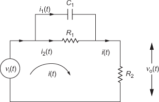
Fig. 11.11 ∣ A simple lead compensator
Applying Kirchoff's current law to the above circuit, we obtain
![]()
 (11.18)
Taking Laplace transform on both sides, we obtain
![]() (11.19)
(11.19)
![]()

Therefore, the transfer function of the above circuit is
 (11.20)
Comparing Eqs. (11.12) and (11.20), we obtain
![]() and
and ![]()
11.4.3 Effects of Lead Compensator
The effects of adding lead compensator to the given system are:
- Damping of the closed-loop system increases since a dominant zero is added to the system.
- Peak overshoot of the system, rise time and settling time of the system decrease and as a result of which the transient response of the system gets improved.
- Gain margin and phase margin of the system get increased.
- Improves the relative stability of the system.
- Increases the bandwidth of the system that corresponds to the faster time response.
11.4.4 Limitations of Lead Compensator
The limitations of adding lead compensator to the given system are:
- Single-phase lead compensator can provide a maximum phase lead of
 . If a phase lead of more than
  is required, multistage compensator must be used.
 - There is always a possibility of reaching the conditionally stable condition even though the desired system requirements are achieved.
11.4.5 Design of Lead Compensator
The objective of designing the lead compensator is to determine the values of ![]() and
and ![]() for an uncompensated system
for an uncompensated system ![]() based on the desired system requirements. The design of lead compensator can be either based on the frequency domain specifications or time- domain specifications. The Bode plot is used for designing the lead compensator based on the frequency domain specifications and root locus technique is used for designing the lead compensator based on the time-domain specifications. Once
based on the desired system requirements. The design of lead compensator can be either based on the frequency domain specifications or time- domain specifications. The Bode plot is used for designing the lead compensator based on the frequency domain specifications and root locus technique is used for designing the lead compensator based on the time-domain specifications. Once ![]() and
and ![]() are determined, the transfer function of the lead compensator
are determined, the transfer function of the lead compensator ![]() can be obtained. The transfer function of the compensated system
can be obtained. The transfer function of the compensated system ![]() . If the Bode plot or root locus technique is plotted for the compensated system, it will satisfy the desired system requirements.
. If the Bode plot or root locus technique is plotted for the compensated system, it will satisfy the desired system requirements.
11.4.6 Design of Lead Compensator Using Bode Plot
Let the open-loop transfer function of the uncompensated system be ![]() . The objective is to design a lead compensator
. The objective is to design a lead compensator ![]() for
for ![]() so that the compensated system
so that the compensated system ![]() will satisfy the desired system requirements. The steps for determining the transfer function of the compensated system
will satisfy the desired system requirements. The steps for determining the transfer function of the compensated system ![]() using Bode plot are explained below:
using Bode plot are explained below:
Step 1:If the open-loop transfer function of the system ![]() has a variable
has a variable ![]() , then
, then ![]() ; otherwise
; otherwise ![]() .
.
Step 2:Depending on the input and TYPE of the system, the variable ![]() present in the open-loop transfer function of the uncompensated system is determined based on either the steady-state error or the static error constant of the system.
present in the open-loop transfer function of the uncompensated system is determined based on either the steady-state error or the static error constant of the system.
The static error constants of the system are
Position error constant, ![]()
Velocity error constant, ![]()
Acceleration error constant, ![]()
The relation between the steady-state error and static error constant based on the TYPE of the system and input applied to the system can be referred to Table 5.5 of Chapter 5.
Step 3:Construct the Bode plot for the uncompensated system with gain ![]() obtained in the previous step and determine the frequency domain specifications of the system (i.e., phase margin, gain margin, phase crossover frequency and gain crossover frequency). Let the phase margin of the uncompensated system be
obtained in the previous step and determine the frequency domain specifications of the system (i.e., phase margin, gain margin, phase crossover frequency and gain crossover frequency). Let the phase margin of the uncompensated system be ![]() .
.
Step 4:Let the desired phase margin of the system be ![]() . With a tolerance
. With a tolerance ![]() , determine
, determine ![]() as
as
![]()
where ![]() to
to ![]() .
.
Step 5:Determine ![]() using
using ![]() .
.
Step 6:Determine ![]() in dB. Let it be
in dB. Let it be ![]() .
.
Step 7:Determine the frequency from the magnitude plot of the uncompensated system for the magnitude of ![]() dB. Let this frequency be the new gain crossover frequency
dB. Let this frequency be the new gain crossover frequency ![]() .
.
Step 8:Determine ![]() using
using ![]() .
.
Step 9: Determine ![]() using
using ![]() .
.
Step 10: Thus, the transfer function of the lead compensator will be determined as 
Step 11: The transfer function of the compensated system will be ![]() . If the Bode plot for the compensated system is drawn, it will satisfy the desired system requirements.
. If the Bode plot for the compensated system is drawn, it will satisfy the desired system requirements.
Flow chart for designing the lead compensator using Bode plot
The flow chart for determining the parameters present in the transfer function of the lead compensator using Bode plot is shown in Fig. 11.12.

Fig. 11.12 ∣ Flow chart for designing the lead compensator using Bode plot
Example 11.3: Consider a unity feedback uncompensated system with the open-loop transfer function as ![]() . Design a lead compensator for the system such that the compensated system has static velocity error constant
. Design a lead compensator for the system such that the compensated system has static velocity error constant ![]() and phase margin pm = 40°.
and phase margin pm = 40°.
Solution:
- Let
 .
. - The value of
 is determined by using
  as
as

Solving the above equation, we obtain
 .
. - 3. The Bode plot for
 H(s) = 1 is drawn.
- Given

- Substituting
 in the above equation, we obtain

- The corner frequency existing in the given system is
 rad/sec
To sketch the magnitude plot:
- The changes in slope at different corner frequencies are given in Table E11.3(a).
Table E11.3(a) ∣ Determination of change in slope at different corner frequencies

- Assume the lower frequency as ωl = 0.1 rad/sec and higher frequency as ωh = 20 rad/sec.
- The values of gain at different frequencies are determined and given in Table E11.3(b).
Table E11.3(b) ∣ Gain at different frequencies

- The magnitude plot of the given system is plotted using Table E11.3(b) and is shown in Fig. E11.3.
To sketch the phase plot:
- (h) The phase angle of the given loop transfer function as a function of frequency is obtained as

- The phase angle at different frequencies is obtained using the above equation and the values are tabulated as shown in Table E11.3(c).
Table E11.3(c) ∣ Phase angle of the system for different frequencies

- (j) The phase plot of the given system is plotted with the help of Table E11.3(c) and is shown in Fig. E11.3.

Fig. E11.3
- (k) The frequency domain specifications of the given system are
Gain crossover frequency,
 rad/sec
Phase crossover frequency,
 rad/sec
Gain margin,
 dB and
Phase margin,

It can be noted that the uncompensated system is stable, but the phase margin of the system is less than the desired phase margin.
- Given
- With tolerance value
 ,
,  is calculated as
i. e.,
 .
. - The value of
 in the lead compensator is determined by using,
  .
.
i.e.,


Solving the above equation, we obtain

- Let
 dB
dB - The new gain crossover frequency
 corresponding to B from the magnitude plot of the uncompensated system is 5 rad/sec.
 - Using
 , determine T as
  .
.
i. e.,
 .
. - The value of
 is determined as
  i.e.,
i.e.,  .
. - The transfer function of the lead compensator is

- Thus, the transfer function of the compensated system is

11.4.7 Design of Lead Compensator Using Root Locus Technique
The desired time-domain specifications that can be specified for designing the lead compensator are peak overshoot, settling time, rise time, damping ratio and undamped natural frequency of the system. The step-by-step procedure for designing the lead compensator for an uncompensated system whose open-loop transfer function is given by ![]() using root locus technique is given below:
using root locus technique is given below:
Step 1: Determine the damping ratio ![]() and undamped natural frequency
and undamped natural frequency ![]() of the system based on the given time-domain specifications.
of the system based on the given time-domain specifications.
Step 2: Determine the dominant closed-loop poles of the system using ![]() or
or ![]() . Let
. Let ![]() and
and ![]() be the dominant closed-loop poles of the system that is marked in s-plane as shown in Fig. 11.13(a).
be the dominant closed-loop poles of the system that is marked in s-plane as shown in Fig. 11.13(a).

Fig. 11.13(a)
Step 3: Determine the angle of the loop transfer function ![]() at any one of the dominant pole i.e., either
at any one of the dominant pole i.e., either ![]() or
or ![]() . Let the angle obtained be
. Let the angle obtained be ![]() degrees i.e.,
degrees i.e., ![]()
Step 4: The angle obtained in the previous step, i.e., ![]() should be an odd multiple of
should be an odd multiple of ![]() . If it is not so, some values of angle can be added or subtracted from
. If it is not so, some values of angle can be added or subtracted from ![]() to make it an odd multiple of
to make it an odd multiple of ![]() . The angle by which
. The angle by which ![]() has to be added or subtracted is obtained using
has to be added or subtracted is obtained using ![]() . The value of
. The value of ![]() is always less than
is always less than ![]() and if
and if ![]() is greater than
is greater than ![]() , then multiple lead compensators can be used.
, then multiple lead compensators can be used.
Step 5: Draw a line parallel to the X-axis from point ![]() to
to ![]() and also join the point
and also join the point ![]() with the origin as shown in Fig. 11.13(b).
with the origin as shown in Fig. 11.13(b).

Fig. 11.13(b)
Step 6: Determine ![]() and using
and using ![]() draw a line from the point
draw a line from the point ![]() that bisects the negative X-axis at point
that bisects the negative X-axis at point ![]() as shown in Fig. 11.13(b).
as shown in Fig. 11.13(b).
Step 7: Draw two lines ![]() and
and ![]() from point P1 such that
from point P1 such that ![]() , which is shown in Fig. 11.13(c).
, which is shown in Fig. 11.13(c).

Fig. 11.13(c)
Step 8: The points ![]() and
and ![]() in the negative real axis corresponds to the pole and zero of the lead compensator respectively.
in the negative real axis corresponds to the pole and zero of the lead compensator respectively.
Step 9: The constants in the lead compensator (![]() and
and ![]() ) are determined by using
) are determined by using ![]() and
and ![]() .
.
Step 10: Using the constants determined in the previous step, the transfer function of the lead compensator is obtained as
 .
.
Step 11: The transfer function of the compensated system is obtained using ![]()
Step 12: The constant ![]() of the system is determined by using
of the system is determined by using ![]() .
.
Step 13: If the root locus of the compensated system is drawn, we can see that the root locus of the compensated system will pass through the dominant closed-loop poles of the system.
The flow chart for designing the lead compensator using the root locus technique is shown in Fig. 11.14.

Fig. 11.14 ∣ Flow chart for designing the lead compensator
Example 11.4 Consider a unity feedback uncompensated system with the open-loop transfer function as ![]() . Design a lead compensator for the system such that the compensated system has damping ratio
. Design a lead compensator for the system such that the compensated system has damping ratio ![]() and un-damped natural frequency
and un-damped natural frequency ![]() rad/sec.
rad/sec.
Solution
- Refer to the solution of Example 11.2 and follow the steps to obtain the root locus of the system.
The complete root locus for the system is shown in Fig. E11.4.
- Using
 and undamped natural frequency
  = 2, the dominant closed-loop poles are
  .
.

Fig. E11.4
- The angle of the system at dominant closed-loop pole is

- Since the angle obtained in the previous step is not an odd multiple of
 , the angle to be contributed by lead compensator is given by
  .
. - A line parallel to the X-axis from point
 to
to  and also the point
  is joined with the origin.
 - The angle
 is determined as
  and using
  , a line from the point
  is drawn which bisects the negative X-axis at point
  .
. - Two lines
 and
and  are drawn from point such that
- The points C and D are the poles and zeros of the lead compensator respectively. Since the zero is at
 and there exists pole-zero cancellation, the zero of lead compensator is taken slightly left of point –1. Let it be
  . Therefore,
  and
and 
- The constants in the lead compensator are determined by using
 and
and  Therefore,
  and
and  .
. - Therefore, the transfer function of lead compensator is

- Thus, the transfer function of the compensated system is
 .
. - Using the magnitude condition,
 , the constant
  is determined as

 .
.Thus, the transfer function of the compensated system is

11.5 Lag–Lead Compensator
In the previous sections, the unique advantages, disadvantages and limitations of the lead compensator and lag compensator have been discussed. Lead compensator will improve the rise time and damping and also affects natural frequency of the system and lag compensator will improve the damping of the system, but it also increases the rise time and settling time. Therefore, lag–lead compensator is a combination of lag and lead compensators which is used for a system to gain the individual advantages of each compensator. Also, the use of both the compensators is necessary for some systems as the desired result cannot be achieved when the compensators are used alone. In general, in lag–lead compensator, the lead compensator is used for achieving a shorter rise time and higher bandwidth and lag compensator is used for achieving good damping for a system.
The general transfer function of the lag–lead compensator is given by
 (11.21)
where ![]() are constants and
are constants and ![]()
The term in Eqn. (11.21) which produces the effect of lead compensator is

The term in Eqn. (11.21) that produces the effect of lag compensator is

The pole-zero configuration of the lag–lead compensator is shown in Fig. 11.15.

Fig. 11.15 ∣ Pole-zero configuration of Gla–le (s)
The Bode plot and polar plot of the lag–lead compensator is shown in Figs. 11.16(a) and 11.16(b) respectively.

(a)

(b)
Fig. 11.16 ∣ Plots of lag–lead compensator
The Bode plot shown in Fig. 11.16(a) is plotted with ![]() and
and ![]() . The conclusion inferred from the Bode plot of the lag compensator shown in Fig. 11.16(a) is that magnitude of lag–lead compensator is zero at low and high frequencies.
. The conclusion inferred from the Bode plot of the lag compensator shown in Fig. 11.16(a) is that magnitude of lag–lead compensator is zero at low and high frequencies.
11.5.1 Electrical Representation of the Lag–Lead Compensator
A simple lag-lead compensator using resistor and capacitor is shown in Fig. 11.17.

Fig. 11.17 ∣ A simple lag–lead compensator
Applying Kirchoff's current law to the above circuit as shown in Fig. 11.17, we obtain
 (11.21)
The output voltage of the circuit is given by
![]() (11.22)
(11.22)
Taking Laplace transform on both sides of the above equations, we obtain
![]() (11.23)
(11.23)

 (11.24)
Substituting Eqn. (11.24) in Eqn. (11.23), we obtain


Simplifying the above equation, we obtain


Therefore, the transfer function of the above circuit is


Therefore,
 (11.25)
Rearranging Eqn. (11.21), we obtain
 (11.26)
Comparing Eqn. (11.26) with Eqn. (11.25), we get
![]() ,
, ![]() ,
,
![]()
![]()
From the above representation, it can be noted that the values of ![]() and
and ![]() should be same for the lag–lead compensator.
should be same for the lag–lead compensator.
11.5.2 Effects of Lag–Lead Compensator
The following are the effects of adding lag–lead compensator to the given system:
- Used when both the fast response and good static accuracy for a system is required.
- Increases low-frequency gain that improves steady state.
- Increases the bandwidth of the system that results in faster response of the system.
11.5.3 Design of Lag–Lead Compensator
The objective of designing the lag–lead compensator is to determine the values of constants (![]() and
and ![]() ) present in the transfer function of a compensator for a uncompensated system
) present in the transfer function of a compensator for a uncompensated system ![]() based on the desired system requirements. The design of lag–lead compensator can be either based on the frequency domain specifications or based on time-domain specifications. The Bode plot is used for designing the lag–lead compensator based on the frequency domain specifications and root locus technique is used for designing the lag-lead compensator based on the time-domain specifications. Once the constant is determined, the transfer function of the lag–lead compensator
based on the desired system requirements. The design of lag–lead compensator can be either based on the frequency domain specifications or based on time-domain specifications. The Bode plot is used for designing the lag–lead compensator based on the frequency domain specifications and root locus technique is used for designing the lag-lead compensator based on the time-domain specifications. Once the constant is determined, the transfer function of the lag–lead compensator ![]() can be obtained. The transfer function of the compensated system is
can be obtained. The transfer function of the compensated system is ![]() ; and if the Bode plot or root locus technique is plotted for the compensated system, it will satisfy the desired system requirements.
; and if the Bode plot or root locus technique is plotted for the compensated system, it will satisfy the desired system requirements.
11.5.4 Design of Lag–Lead Compensator Using Bode Plot
Consider the open-loop transfer function of the uncompensated system be ![]() . The objective is to design a lag–lead compensator
. The objective is to design a lag–lead compensator ![]() for
for ![]() so that the compensated system
so that the compensated system ![]() will satisfy the desired system requirements. The step by step procedure for determining the transfer function of the compensated system
will satisfy the desired system requirements. The step by step procedure for determining the transfer function of the compensated system ![]() using Bode plot is explained below:
using Bode plot is explained below:
Step 1:If the open-loop transfer function of the system ![]() has a variable
has a variable ![]() , then
, then ![]() ; otherwise
; otherwise ![]() .
.
Step 2:Depending on the input and TYPE of the system, the variable ![]() present in the open-loop transfer function of the uncompensated system is determined based on either the steady-state error or the static error constant of the system.
present in the open-loop transfer function of the uncompensated system is determined based on either the steady-state error or the static error constant of the system.
The static error constants of the system are
Position error constant, ![]()
Velocity error constant, ![]()
Acceleration error constant, ![]()
The relation between the steady-state error and static error constants based on the TYPE of the system and input applied to the system can be referred to Table 5.5 of Chapter 5.
Step 3:Construct the Bode plot for the uncompensated system with gain ![]() obtained in the previous step and determine the frequency domain specifications of the system (i.e., phase margin, gain margin, phase crossover frequency and gain crossover frequency). Let the phase margin, gain margin, phase crossover frequency and gain crossover frequency of the uncompensated system be
obtained in the previous step and determine the frequency domain specifications of the system (i.e., phase margin, gain margin, phase crossover frequency and gain crossover frequency). Let the phase margin, gain margin, phase crossover frequency and gain crossover frequency of the uncompensated system be ![]() and
and ![]() .
.
Step 4:Let the desired phase margin of the system be ![]() .
.
Step 5:Determine ![]() using
using ![]() and
and ![]() .
.
Step 6:Determine the frequency of the system at which the phase plot of the uncompensated system is ![]() . Let the frequency be the new gain crossover frequency
. Let the frequency be the new gain crossover frequency ![]() .
.
Step 7:Determine the constant,  .
.
Step 8:Determine the transfer function of the lag compensator as  .
.
Step 9:Determine the magnitude of uncompensated system at ![]() . Let it be
. Let it be ![]() dB.
dB.
Step 10:Draw a line from the point (![]() ) so that it bisects the
) so that it bisects the ![]() dB line and
dB line and ![]() dB line and determine the frequencies corresponding to the intersection points. Let
dB line and determine the frequencies corresponding to the intersection points. Let ![]() rad/sec and
rad/sec and ![]() rad/sec be the frequencies at which the line intersects
rad/sec be the frequencies at which the line intersects ![]() dB line and
dB line and ![]() dB line respectively.
dB line respectively.
Step 11:Determine the constants ![]() and
and ![]() using
using ![]() and
and ![]() .
.
Step 12:Thus, the transfer function of the lag–lead compensator will be determined as 
Step 10:The transfer function of the compensated system will be ![]() . If the Bode plot for the compensated system is drawn, it will satisfy the desired system requirements.
. If the Bode plot for the compensated system is drawn, it will satisfy the desired system requirements.
Flow chart for designing the lag–lead compensator using Bode plot
The flow chart for determining the parameters present in the transfer function of the lag–lead compensator using Bode plot is shown in Fig. 11.18.

Fig. 11.18 ∣ Flow chart for designing the lag–lead compensator using Bode plot
Example 11.5: Consider a unity feedback uncompensated system with the open-loop transfer function as ![]() . Design a lag–lead compensator for the system such that the compensated system has static velocity error constant
. Design a lag–lead compensator for the system such that the compensated system has static velocity error constant ![]() , gain margin
, gain margin ![]() dB and phase margin
dB and phase margin ![]() °.
°.
Solution:
- Let
 .
. - The gain
 is determined by using
  as
as

Solving the above equation, we obtain
 .
. - The Bode plot for
 H(s) = 1 is drawn.
- Given

- Substituting
 in the above equation, we obtain

- The corner frequencies existing in the given system are
 rad/sec and
  rad/sec.
To sketch the magnitude plot:
- The changes in slope at different corner frequencies are given in Table E11.5(a).
Table E11.5(a) ∣ Determination of change in slope at different corner frequencies

- Assume the lower frequency as
 = 0.1 rad/sec and higher frequency as
  = 20 rad/sec.
 - The gain at different frequencies are determined and given in Table E11.5(b).
- The magnitude plot of the given system is plotted using Table E11.1(b) and is shown in Fig. E11.5.
Table E11.5(b) ∣ Gain at different frequencies

To sketch the phase plot:
- The phase angle of the given loop transfer function as a function of frequency is obtained as

- The phase angle at different frequencies is obtained using the above equation and the values are tabulated as shown in Table E11.5(c).
Table E11.5(c) ∣ Phase angle of the system for different frequencies

- The phase plot of the given system is plotted with the help of Table E11.5(c) and is shown in Fig. E11.5.

Fig. E11.5
- The frequency domain specifications of the given system are:
Gain crossover frequency,
 rad/sec.
Phase crossover frequency,
 rad/sec.
Gain margin,
 dB
dBPhase margin,
 .
.It is to be noted that the uncompensated system is stable, but the phase margin of the system is less than the desired phase margin which is
 .
.
- Given
- The desired phase margin for the compensated system is
 .
. - Using
 and
and  ,
,  is determined as 7.54.
 - Let

- The time constant of lag compensator is determined as

- Therefore, the transfer function of lag compensator is
 .
. - The magnitude of the system at
 dB.
dB. - If the slope of +20 dB/decade is drawn from (1.4 rad/sec, –14 dB), the slope cuts the 0 dB line and –20 dB line at
 rad/sec and at
  rad/sec respectively.
 - Thus, the transfer function of the lead portion of the lag–lead compensator is

- Therefore, the transfer function of the lag–lead compensator is

11.5.5 Design of Lag–Lead Compensator Using Root Locus Technique
The transfer function of the lag–lead compensator is given by  ,
, ![]() and
and ![]() . The design of lag–lead compensator using root locus technique is based on the relation between β and γ. Therefore, two different cases exist in designing the lag–lead compensator for a system.
. The design of lag–lead compensator using root locus technique is based on the relation between β and γ. Therefore, two different cases exist in designing the lag–lead compensator for a system.
Case 1: When ![]()
The step-by-step procedure for designing the lag–lead compensator using root locus technique when ![]() is discussed below.
is discussed below.
Step 1:Determine the damping ratio ![]() and undamped natural frequency
and undamped natural frequency ![]() of the system based on desired time-domain specifications of the system.
of the system based on desired time-domain specifications of the system.
Step 2:Determine the dominant pole of the system using ![]() . Let the dominant poles of the system be
. Let the dominant poles of the system be ![]() and
and ![]() .
.
Step 3:Follow the procedure shown in Fig. 11.14 in determining the constants of lead compensator, i.e., ![]() and
and ![]() .
.
Step 4:Determine the constant ![]() using the condition
using the condition  .
.
Step 5:Using the static error constant and constants determined in the previous steps, the value of ![]() is determined.
is determined.
Step 6:Determine ![]() using
using 
Step 7:Now, determine the transfer function of the lag–lead compensator ![]() .
.
Step 8:The transfer function of the compensated system is ![]() .
.
Flow chart for designing the lag–lead compensator using root locus technique when 
The step-by-step procedure for designing the lag–lead compensator using root locus technique when ![]() is shown in Fig. 11.19.
is shown in Fig. 11.19.

Fig. 11.19 ∣ Flow chart for designing lag-lead compensator when ![]()
Case 2: When ![]()
The step-by-step procedure for designing the lag–lead compensator using root locus technique when ![]() is discussed below:
is discussed below:
Step 1:Determine the damping ratio ![]() and undamped natural frequency
and undamped natural frequency ![]() of the system based on desired-time domain specifications of the system.
of the system based on desired-time domain specifications of the system.
Step 2:Determine the dominant pole of the system using ![]() . Let the dominant poles of the system be
. Let the dominant poles of the system be ![]() and
and ![]() .
.
Step 3:Using the formula for static error constant, determine the value of constant ![]() .
.
Step 4:Determine the angle of the loop transfer function ![]() at any one of the dominant pole, i.e., either
at any one of the dominant pole, i.e., either ![]() or
or ![]() . Let the angle obtained be
. Let the angle obtained be ![]() degrees.
degrees.
Step 5:The angle obtained in the previous step, i.e., ![]() should be an odd multiple of
should be an odd multiple of ![]() . If it is not so some value of angle can be added or subtracted from
. If it is not so some value of angle can be added or subtracted from ![]() to make it an odd multiple of
to make it an odd multiple of ![]() . The angle by which
. The angle by which ![]() has to be added or subtracted is obtained using the formula,
has to be added or subtracted is obtained using the formula, ![]() . The value of
. The value of ![]() is always less than
is always less than ![]() and if
and if ![]() is greater than
is greater than ![]() , then multiple lead compensators can be used.
, then multiple lead compensators can be used.
Step 6:Determine the length of points OA and OB such that  and
and ![]() . The points in the s-plane are shown in Fig. 11.20.
. The points in the s-plane are shown in Fig. 11.20.

Fig. 11.20
Step 7:Determine the constants ![]() and
and ![]() using the formula
using the formula ![]() and
and ![]() .
.
Step 8:Determine ![]() using
using  .
.
Step 9:The transfer function of the lag–lead compensator is determined as  .
.
Flow chart for designing the lag–lead compensator using root locus technique when 
The step-by-step procedure for designing the lag–lead compensator using root locus technique when ![]() is shown in Fig. 11.21.
is shown in Fig. 11.21.

Fig. 11.21 ∣ Flow chart for designing lag-lead compensator when ![]()
Review Questions
- What is the principle of compensation? What are the types of compensation?
- Draw the electric network that could be used for phase lag compensation. Derive its transfer function and hence obtain Bode plot.
- Derive the transfer function of phase lag network and sketch the frequency response curves to the same.
- Under what circumstances a lag compensator is preferred? Why?
- What are the steps involved in designing a phase-lag compensator?
- What are the advantages of the lag compensator?
- Give the diagram to lead compensator.
- How are lag and lead compensators realized using electric circuits?
- Under what circumstances is a lead compensator preferred? Why?
- Show how a phase lead compensation network can be designed.
- Derive the transfer function of phase lead network and obtain the necessary expressions for system compensation with lead network.
- Enumerate the design steps involved in the phase lead compensation.
- Compare lead, lag and lag-lead compensation.
- Write a short note on series compensation.
- Explain the features of feedback compensation.
- Write short notes on the feedback compensation.
- Show the realization of a lag–lead compensator using electrical circuit.
- Write a note on series compensation using lag-lead networks.
- What is meant by feedback compensation?
- Consider a TYPE 1 system with open loop transfer function
 Design a lag compensator to meet the following specifications:
Damping ratio

Settling time = 10 sec
Velocity error constant

- For a unity feedback system with open-loop gain
 design a compensator to meet the following:
Damping ratio

Settling time

Velocity error co-efficient

- Determine the transfer function of a lead compensator that will provide a phase lead of
 and gain of 8 db at
- A unity feedback network system has
 . Design a compensator network for the system so that the static velocity error constant
  and the phase margin is at least
  .
. - Design a lead compensator for a unity-feedback open-loop transfer function
 to meet the following specifications:
Damping ratio

Settling time

and Velocity error constant

- Design a lag compensator for the system
 with unity feedback to achieve the following specifications:
Velocity error constant

and phase margin

- A unity feedback system with the open-loop transfer function
 is required to have (i) velocity error constant
  and (ii) phase margin
  . Design a suitable phase lag compensator to meet the above specifications.
 - Explain the steps involved in the time-domain design of phase lead compensation.
- The open-loop transfer function of a system is given as
 . Design a lead compensation for the system to meet the following specifications:
(i) Setting time 4 sec and (ii) peak over shoot for step input
 %.
%. - A unity feedback system with forward path transfer function
 is to have (i) the velocity error constant
  and (ii) phase margin
  . Design a suitable phase-lag compensator to meet the above specifications.
 - A unity feedback system with
 is to be compensated to have a phase margin of
  without sacrificing the velocity error constant. Design a suitable lag network and compute the component values for a suitable impedance level.
 - Design a compensator for a unity feedback system with open-loop gain given by
 so that the static velocity error constant is
  and the dominant closed-loop poles are located at
  .
. - For the system whose open-loop transfer function is
 , design a compensator so that the damping ratio is 0.5 and undamped natural frequency is 2.
 - Design a compensator for the system with
 to have a phase margin of
  .
.