
In this section, I’ll show you how to expand the capabilities of your processor by interfacing it to bus-based memories and peripherals. Before we do anything else, let’s take a quick tour of those mysterious timing diagrams found in datasheets and understand what they all mean.
A timing diagram is
a representation of the
input and output signals of a device
and how they relate to one another. In essence, it indicates when a
signal needs to be asserted and when you can expect a response from
the device. For two devices to interact, the timing of signals
between the two must be compatible, or you must provide additional
circuitry to make them compatible.
Timing diagrams scare and confuse many people and are often ignored completely. Ignoring device timing is a sure way of guaranteeing that your system will not work! However, they are not that hard to understand and use. If you want to design and build reliable systems, remember that timing is everything!
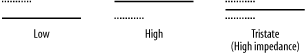
Digital signals may be in one of three states, high, low, or high impedance (tristate). On timing diagrams for digital devices, these states are represented as shown in Figure 6-11.
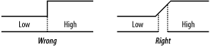
Transitions from one state to another are shown in Figure 6-12.
The last waveform (High-High/Low) indicates that a signal is high and, at a given point in time, may either remain high or change to low. Similarly, a signal line that is tristate may go low, high, or either high or low depending on the state of the system. An example of this is a data line, which will be tristate until an information transfer begins. At this point in time, it will either go high (data = 1) or low (data = 0) (Figure 6-13).

The waveforms in Figure 6-14 indicate a change from tristate to high/low and back again. These symbols indicate that the change may happen anywhere within a given range of time but will have happened by a given point in time.

The waveform in Figure 6-15 indicates that a signal may/will change at a given point in time. The signal may have been high and will either remain high or go low. Alternatively, the signal may have been low and will either remain low or go high.
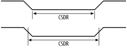
The impression given in many texts on digital circuits is that a change in signal state is instantaneous. This is not so. A transition is never instant; it can be several nanoseconds in duration, and there is considerable variation between different devices (Figure 6-16). The datasheet for each component will detail the transition times for that particular device.
Datasheets from component manufacturers specify timing information for devices. An example timing diagram for an imaginary device is shown in Figure 6-17.

The diagram shows the relationship between input signals to the device (such as CS) and outputs from the device (such as Data). The numbers on the diagram are references to timing information within tables. They do not represent timing directly. Table 6-2 shows how a datasheet might list the timing parameters.
Table 6-2. Example timing parameters
|
Ref |
Description |
Min |
Max |
Units |
|---|---|---|---|---|
|
1 |
CS hold time |
60 |
ns | |
|
2 |
CS to data valid |
30 |
ns | |
|
3 |
Data hold time |
5 |
10 |
ns |
Timing reference 1 (the first row of Table 6-2) shows how long CS must be held low. In this instance, it is a minimum of 60ns. This means that the device won’t guarantee that CS will be recognized unless it is held low for more than this time. There is no maximum specified. This means that it doesn’t matter if CS is held low for longer than 60ns. The only requirement is that it is low for a minimum of 60ns.
Timing reference 2 shows how long it takes the device to respond to CS going low. From when CS goes low until this device starts outputting data is a maximum of 30ns. What this means is that 30ns after CS goes low, the device will be driving valid data onto the data bus. It may start driving data earlier than 30ns. The only guarantee is that it will take no longer than 30ns for this device to respond.
Timing reference 3 specifies when the device will stop driving data once CS has been negated. This reference has a minimum of 5ns and a maximum of 10ns. This means that data will be held valid for at least 5ns, but no more than 10ns, after CS negates.
Some manufacturers use numbers to reference timing, others may use labels (Figure 6-18).

Some manufacturers will specify timing from when a signal becomes valid until it is no longer valid. Others specify timing from the middle of a transition to the middle of the next transition (Figure 6-19).
So, with all that in mind, let’s look at the timing for a real processor. Different processor architectures have different signals and different timing, but once you understand one, the basic principles can be applied to all. Since most small microcontrollers don’t have external buses, the choice is very limited. We’ll look at the one, and only, AVR with an external bus—the AT90S8515. In the PIC world, the PIC17C44 is capable of bus-based interfacing.
A
memory cycle (also
known as a machine cycle or processor
cycle) is
defined as the period of time it takes
for a processor to initiate an access to memory (or peripheral),
perform the transfer, and terminate the access. The memory cycle
generated by a processor is usually of a fixed period of time (or
multiples of a given period) and may take several (processor) clock
cycles to complete.
Memory cycles usually fall into two categories, the read
cycle and the write cycle. The memory
or device that is being accessed requires that the data is held valid
for a given period after it has been selected and after a read or
write cycle has been identified. This places constraints on the
system designer. There is a limited time in which any glue logic
(interface logic between the processor and other devices) must
perform its function, such as selecting which external device is
being accessed. The setup times must be met. If they are not, the
computer will not function. The glue logic that monitors the address
from the processor and uniquely selects a device is
known
as an address decoder. We’ll
take a closer look at address decoders shortly.
Timing is probably the most critical aspect of computer design. For example, if a given processor has a 150ns cycle time and a memory device requires 120ns from when it is selected until when it has completed the transfer, this leaves only 30ns at the start of the cycle in which the glue logic can manipulate the processor signals. A 74LS series TTL gate has a typical propagation delay of 10ns. So, in this example, an address decoder implemented using any more than two 74LS gates (in sequence) is cutting it very fine.
A synchronous
processor has memory cycles of a
fixed duration, and all processor timing is directly related to the
clock. It is assumed that all devices in the system are capable of
being accessed and responding within the set time of the memory
cycle. If a device in the system is slower than
that allowed by the memory cycle time, logic is required to pause the
processor’s access, thus giving the slow device time
to respond. Each clock cycle within this pause is known as a
wait state
. Once sufficient time has elapsed (and
the device is ready), the processor is released by the logic and
continues with the memory cycle. Pausing the processor for slower
devices is known as inserting wait states. The
circuitry that causes a processor to hold is known as a
wait-state generator. A wait state generator is
easily achieved using a series of flip-flops acting as a simple
counter. The generator is enabled by a processor output indicating
that a memory cycle is beginning and is normally reset at the end of
the memory cycle to return it to a known state. (Some processors come
with internal, programmable wait-state generators.)
An asynchronous processor does not terminate its memory cycle within a given number of clock cycles. Instead, it waits for a transfer acknowledge assertion from the device or support logic to indicate that the device being accessed has had sufficient time to complete its part in the memory cycle. In other words, the processor automatically inserts wait states in its memory cycle until the device being accessed is ready. If the processor does not receive an acknowledge, it will wait indefinitely. Many computer systems using asynchronous processors have additional logic to cause the processor to restart if it waits too long for a memory cycle to terminate. An asynchronous processor can be made into a synchronous processor by tying the acknowledge line to its active state. It then assumes that all devices are capable of keeping up with it. This is known as running with no wait states.
Most microcontrollers are synchronous, whereas most larger processors are asynchronous. The AT90S8515 is a synchronous processor, and it has an internal wait-state generator capable of inserting a single wait state.
Figure 6-20 shows an AT90S8515 processor with support components. The AT90S8515 has an address bus, a data bus, and a control bus that it brings to the outside world for interfacing. Since this processor has a limited number of pins, these buses share pins with the digital I/O ports (port A and port B) of the processor. A bit in a control register determines whether these pins are I/O or bus pins. Now, a 16-bit address bus and an 8-bit data bus add up to 24 bits, but ports A and B have only 16 bits between them. So how does the processor fit 24 bits into 16? It multiplexes the lower half of the address bus with the data bus. At the start of a memory access, port A outputs address bits A0..A7. The processor provides a control line, ALE (Address Latch Enable), which is used to control a latch, such as a 74HCT573 (shown on the right in Figure 6-20). As ALE falls, the latch grabs and holds the lower address bits. At the same time, port B outputs the upper address bits, A8..A15. These are valid for the entire duration of the memory access. Once the latch has acquired the lower address bits, port A then becomes the data bus for information transfer between the processor and an external device. Also shown in Figure 6-20 are the crystal circuit, the In-System Programming port, decoupling capacitors for the processor’s power supply, and net labels for other important signals.


The timing diagrams for an AT90S8515 are shown in Figure 6-21. The cycle T3 exists only when the processor’s wait state generator is enabled.

Now, let’s look at these signals in more detail. (We’ll see later how you actually work with this information. For the moment, we’re just going to “take a tour” of the timing diagrams.) The numbers for the timing information can be found in the datasheet, available from ATMEL’s web site. Figure 6-22 shows the timing information as presented in the ATMEL datasheet, complete with timing references.
The references are looked up in the appropriate table in the processor’s datasheet (Table 6-3).
Table 6-3. Timing parameters
|
Symbol |
Parameter |
8MHz oscillator |
Variable oscillator | ||||
|---|---|---|---|---|---|---|---|
|
Min |
Max |
Min |
Max |
Unit | |||
|
0 |
1/tCLCL |
Oscillator frequency |
0.0 |
8.0 |
MHz | ||
|
1 |
tLHLL |
ALE pulse width |
32.5 |
0.5tCLCL-30.0 |
ns | ||
|
2 |
tAVLL |
Address valid A to ALE low |
22.5 |
0.5tCLCL-40.0 |
ns | ||
|
3a |
tLLAX_ST |
Address hold after ALE low, ST/STD/STS instructions |
67.5 |
0.5tCLCL-50.0 |
ns | ||
|
3b |
tLLAX_LD |
Address hold after ALE low, LD/LDD/LDS instructions |
15.0 |
15.0 |
ns | ||
|
4 |
tAVLLC |
Address valid C to ALE low |
22.5 |
0.5tCLCL-40.0 |
ns | ||
|
5 |
tAVRL |
Address valid to RD low |
95.0 |
1.0tCLCL-30.0 |
ns | ||
|
6 |
tAVWL |
Address valid to WR low |
157.5 |
1.5tCLCL-30.0 |
ns | ||
|
7 |
tLLWL |
ALE low to WR low |
105.0 |
145.0 |
1.0tCLCL-20.0 |
1.0tCLCL+20.0 |
ns |
|
8 |
tLLRL |
ALE low to RD low |
42.5 |
82.5 |
0.5tCLCL-20.0 |
0.5tCLCL+20.0 |
ns |
|
9 |
tDVRH |
Data setup to RD high |
60.0 |
60.0 |
ns | ||
|
10 |
tRLDV |
Read low to data valid |
70.0 |
1.0tCLCL-55.0 |
ns | ||
|
11 |
tRHDX |
Data hold after RD high |
0.0 |
0.0 |
ns | ||
|
12 |
tRLRH |
PD pulse width |
105.0 |
1.0tCLCL-20.0 |
ns | ||
|
13 |
tDVWL |
Data setup to WR low |
27.5 |
0.5tCLCL-35.0 |
ns | ||
|
14 |
tWHDX |
Data hold after WR high |
0.0 |
0.0 |
ns | ||
|
15 |
tDVWH |
Data valid to WR high |
95.0 |
1.0tCLCL-30.0 |
ns | ||
|
16 |
tWLWH |
WR pulse width |
42.5 |
0.5tCLCL-20.0 |
ns | ||
The system clock, ϕ, is shown at the top of both diagrams for reference, since all processor activity relates to this clock. The period of the clock is designated in the ATMEL datasheet as tCLCL [3] and is equal to 1/frequency. For an 8MHz clock, this is 125ns. T1, T2, and T3 each has a width of tCLCL.
No processor cycle exists in isolation. There is always[4] a preceding cycle and following
cycle. We can see this in the timing diagrams. At the start of the
cycles, the address from the previous access is still present on the
address bus. On the falling edge of the clock, in cycle T1, the
address bus changes to become the valid address required for this
cycle. Port A presents address bits A0..A7, and port B presents
A8..A15. At the same time, ALE goes
high, releasing the external address latch in preparation for
acquiring the new address from port A. ALE stays high for 0.5 x tCLCL - 30ns. So, for example, with an AT90S8515 running at 8MHz,
ALE stays high for 32.5ns. ALE falls, causing the external latch to
acquire and hold the lower address bits. Prior to ALE falling, the address bits will have been
valid for 0.5 x tCLCL - 40ns or, in other words,
40ns before the system clock rises at the end of the T1 period. After
ALE falls, the lower address bits
will be held on port A for 0.5 x tCLCL + 5ns, for
a write cycle, before changing to data bits. For a read cycle, they
are held for a minimum of 15ns only. The reason this is so much
shorter for a read cycle is that the processor wishes to free those
signal pins as soon as possible. Since this is a read cycle, an
external device is about to respond, which means the processor needs
to get out of the way as soon as it can.
For a write cycle, tCLCL - 20ns after ALE goes low, the write strobe,
WR, goes low. This
indicates to external devices that the processor has output valid
data on the data bus.
WR will be low for
0.5 x tCLCL - 20ns. This time is to allow the
external device to prepare to read in (latch) the data. On the rising
edge of
WR, the
external device is expected to latch the data presented on the data
bus. At this point, the cycle completes, and the next cycle is about
to begin.
For a read cycle, the read strobe,
RD, goes low 0.5 x tCLCL - 20ns after ALE
is low.
RD will
be low for tCLCL - 20ns. During this time, the
external device is expected to drive valid data onto the data bus. It
can present data any time after
RD goes low, as long as
data is present and stable at least 60ns before
RD goes high again. At
this point, the processor latches the data from the external device,
and the read cycle terminates. Note that many processors may not have
a separate
read enable signal, so this
must be generated by external logic, based on the premise that if the
cycle is not a write cycle, it must be a read cycle.
So, that is how an AT90S8515 expects to access any external device attached to its buses, whether those devices are memory chips or peripherals. But how does it work in practice? Let’s look at designing[5] a computer based on an AT90S8515, with some external devices. For this example, we will interface the processor to a static RAM and some simple latches that we could use to drive banks of LEDs.
To the processor, its address space is one big linear region. Although there may be numerous devices within that space, both internal to the processor and external, it makes no distinction between devices. The processor simply performs memory accesses with the address space. It is up to the system designer (that’s you) to allocate regions of memory to each device and then to provide address decode logic. The address decoder takes the address provided by the processor during an external access and uniquely selects the appropriate device (Figure 6-23). For example, if we have a RAM occupying a region of memory, any address from the processor corresponding to within that region should select the RAM and not select any other device. Similarly, any address outside that region should leave the RAM unselected.

The allocation of devices within an address space is known as a
memory map or address map.
The address spaces for an AT90S8515 processor are shown in Figure 6-24. Any device we interface to the processor must
be within the data memory space. Thus, we can ignore the
processor’s internal program memory. As the
processor is a Harvard architecture, the program space is a
completely separate address space. Within the 64K data space lie the
processor’s internal resources—the working
registers, the I/O registers and the internal 512 bytes of SRAM.
These occupy the lowest addresses within the space. Any address above
0x0260 is ours to play with. (Not all processors have resources that
are memory mapped, and in those cases the entire memory space is
usable by external devices.)

Now, our first task is to allocate the remaining space to the
external devices. Since the RAM is 32K in size, it makes sense to
place it within the upper half of the address space (0x8000-0xFFFF).
Address decoding becomes much easier if devices are placed on neat
boundaries. Placing the RAM between addresses 0x8000 and 0xFFFF
leaves the lower half of the address space to be allocated to the
latches and the processor’s internal resources. Now
a latch need occupy only a single byte of memory within the address
space. So, if we have three latches, we need only 3 bytes of the
address space to be allocated. This is known as explicit
address decoding. However, there’s a good
reason not to be so efficient with our address allocation. Decoding
the address down to 3 bytes would require an address decoder to use
14 bits of the address. That’s a lot of
(unnecessary) logic to just select three devices. A better way is
simply to divide the remaining address space into four, allocating
three regions for the latches and leaving the fourth unused (for the
processor’s internal resources). This is known as
partial address decoding and is much more
efficient. The trick is to use the minimal amount of address
information to decode for your devices.
Our address map allocated to our static RAM and three latches is shown in Figure 6-25. Note that the lowest region leaves the addresses in the range 0x0260 to 0x1FFF unused.

Any address within the region 0x2000 to 0x3FFF will select Latch0,
even though that latch only needs 1 byte of space. Thus, the device
is said to be mirrored within that space. For
simplicity in programming, you normally just choose an address
(0x2000, say) and use that within your code. But you could just as
easily use address 0x290F, and that would work too.
We now have our memory map, and we need to design an address decoder. We start by tabling the devices, along with their addresses (Table 6-4). We need to look for which address bits are different between the devices and which address bits are common within a given device’s region.
Table 6-4. Address table
|
Device |
Address range |
A15 .. A0 |
|---|---|---|
|
Unused |
0x0000-0x1FFF |
0000 0000 0000 0000 0000 0001 1111 1111 1111 1111 |
|
Latch0 |
0x2000-0x3FFF |
0010 0000 0000 0000 0000 0011 1111 1111 1111 1111 |
|
Latch1 |
0x4000-0x5FFF |
0100 0000 0000 0000 0000 0101 1111 1111 1111 1111 |
|
Latch2 |
0x6000-0x7FFF |
0110 0000 0000 0000 0000 0111 1111 1111 1111 1111 |
|
RAM |
0x8000 - 0xFFFF |
1000 0000 0000 0000 0000 1111 1111 1111 1111 1111 |
So, what constitutes a unique address combination for each device?
Looking at the table, we can see that for the RAM, address bit (and
address signal) A15 is high, while
for every other device it is low. We can therefore use A15 as the trigger to select the RAM. For the
latches, address bits A15, A14, and A13
are critical. So we can redraw our table to make it clearer. (This is
the more common way of doing an address table—Table 6-5.) An x means a
“don’t-care” bit.
Table 6-5. Simplified address table
|
Device |
Address range |
A15 .. A0 |
|---|---|---|
|
Unused |
0x0000-0x1FFF |
000x xxxx xxxx xxxx xxxx |
|
Latch0 |
0x2000-0x3FFF |
001x xxxx xxxx xxxx xxxx |
|
Latch1 |
0x4000-0x5FFF |
010x xxxx xxxx xxxx xxxx |
|
Latch2 |
0x6000-0x7FFF |
011x xxxx xxxx xxxx xxxx |
|
RAM |
0x8000-0xFFFF |
1xxx xxxx xxxx xxxx xxxx |
Therefore, to decode the address for the RAM, we simply need to use A15. If A15 is high, the RAM is selected. If A15 is low, then one of the other devices is selected and the RAM is not. Now, the RAM has a chip select ( CS) that is low active. So when A15 is high, CS should go low. So, our address decoder for the RAM is simply to invert A15, using an inverter chip such as a 74HCT04 (Figure 6-26). The chip select signal is commonly labeled after the device it is selecting. Hence, our chip select to the RAM is labeled RAM.
Note that for the RAM to respond, it needs both a chip select and either a read or write strobe from the processor. All other address lines from the processor are connected directly to the corresponding address inputs of the RAM (Figure 6-27).

Now, for the other four regions, A15 must be low, and A14 and A13 are sufficient to distinguish between the devices. Our address decoder, using discrete logic, would need several gates and would be messy. There’s a simpler way. We can use a 74HCT139[6] decoder, which will take two address inputs (A and B) and gives us four unique, low-active chip select outputs (labeled Y0..Y3). So, our complete address decoder for the computer is shown in Figure 6-28.

The 74HCT139 uses A15 (low) as an enable (input G), and in this way, A15 is included as part of the address decode. If we needed to decode for eight regions instead of four, we could have used a 74HCT138 decoder, which takes three address inputs and gives us eight chip selects.
The interface between the processor and an output latch is simple. We can use the same type of latch (a 74HCT573) that we used to demultiplex the address. Such an output latch could be used in any situation in which we need some extra digital outputs. In the example circuit shown in Figure 6-29, I’m using the latch to control a bank of eight LEDs.

The output from our 74HCT139 address decoder is used to drive the LE (Latch Enable) input of the 74HCT573. Whenever the processor accesses the region of memory space allocated to this device, the address decoder triggers the latch to acquire whatever is on the data bus. And, so, the processor simply writes a byte to any address in this latch’s address region, and that byte is acquired and output to the LEDs. (Writing a 0 to a given bit location will turn a LED on; writing a 1 will turn it off.)
Note that the latch’s output enable ( OE) is permanently tied to ground. This means that the latch is always displaying the byte that was last written to it. This is important as we always want the LEDs to display and not just transitorily blink on while the processor is accessing them.
Using the 74HCT139 in preference to discrete logic gates makes our design much simpler, but there’s an even better way to implement system glue.
Support logic is rarely implemented using individual gates. More common is programmable logic (PALs, LCAs, or PLDs)[7] to implement the miscellaneous glue functions that a computer system requires. Such devices are fast, take up relatively little space, have low power consumption, and as they are reprogrammable, make system design much easier and more versatile.
A wide range of devices is available, from simple chips that can be used to implement glue logic (just as we are about to do) to massive devices with hundreds of thousands of gates.
Tip
Altera (http://www.altera.com),
Xilinx (http://www.xilinx.com),
Lattice Semiconductor (http://www.latticesemi.com), and Atmel are
some manufacturers to investigate for large-scale programmable logic.
These big chips are sophisticated enough to contain entire computer
systems. Soft cores
are processor designs implemented in
gates and suitable for incorporating into these logic devices. You
can also get serial interfaces, disk controllers, network interfaces,
and a range of other peripherals, all for integration into one of
these massive devices. Of course, it’s also fun to
experiment and design your own processor from the ground up.
Each chip family requires its own suite of development tools. These allow you to create your design (using either schematics or some programming language such as VHDL) to simulate the system and finally to download your creation into the chip. You can even get C compilers for these chips that will take an algorithm and convert it, not into machine code, but into gates. What was software now runs, not on hardware, but as hardware. Sounds cool, but the tools required to play with this stuff can be expensive. If you just want to throw together a small, embedded system, they are probably out of your price range. For what we need to do for our glue logic, such chips are overkill.
Since our required logic is simple, we will use a simple (and cheap) PAL that can be programmed using freely available, public-domain software.
PALs are configured using equations to represent the internal logic: + represents OR, * represents AND, and / represents NOT. (These symbols are the original operator symbols that were used in Boolean logic. If you come from a programming background, these symbols may seem strange to you. You will be used to seeing |, &, and !.) The equations are compiled using software such as PALASM, ABEL, or CUPL, to produce a JED file. This is used by a device known as a PAL burner to configure the PAL. In many cases, standard EPROM burners will also program PALs.
PALs have pins for input, pins for output, and pins that can be configured as either input or output. Most of the PAL’s pins are available for your use. In your PAL source code file (PDS file), you declare which pins you are using and label them. This is not unlike declaring variables in program source code, except that instead of allocating bytes of RAM, you’re allocating physical pins of a chip. You then use those pin labels within equations to specify the internal logic. Our address decoder, implemented in a PAL, would have the following equations to specify the decode logic:
RAM = /A15
LATCH0 = /(/A15 * /A14 * A13)
LATCH1 = /(/A15 * A14 * /A13)
LATCH2 = /(/A15 * A14 * A13)
I have (deliberately) written the equations in a form that makes it easier to compare with the address tables listed previously. You could simplify these equations, but there is no need. Just as an optimizing C compiler will simplify (and speed up) your program code, so too will PALASM rework your equations to optimize them for a PAL.
A PDS file to program a 22V10 PAL for the preceding address decode might look something like:
TITLE decoder.pds          ; name of this file
PATTERN
REVISION 1.0
AUTHOR John Catsoulis
COMPANY Embedded Pty Ltd
DATE June 2002

CHIP decoder PAL22V10      ; specify which PAL device you
                           ; are using and give it a name ("decoder")

PIN   2   A15              ; pin declarations and allocations
PIN   3   A14
PIN   12  LATCH0
PIN   13  LATCH1
PIN   14  LATCH2
PIN   15  RAM

EQUATIONS                  ; equations start here

RAM = /A15
LATCH0 = /(/A15 * /A14 * A13)
LATCH1 = /(/A15 * A14 * /A13)
LATCH2 = /(/A15 * A14 * A13)
The advantages of using a PAL for system logic are two-fold. The PAL equations may be changed to correct for bugs or design changes. The propagation delays through the PAL are of a fixed and small duration (no matter what the equations), which makes analyzing the overall system’s timing far simpler. For very simple designs, it probably doesn’t make a lot of difference whether you use PALs or individual chips. However, for more complicated designs, programmable logic is the only option. If you can use programmable logic devices in preference to discrete logic chips, please do so. They make life much easier.
Now that we have finished our logic design, the question is: will it actually work? It’s time (pardon the pun) to work through the numbers and analyze the timing. This is the least fun, and most important, part of designing a computer.
We start with the signals (and timing) of the processor, then add in the effects of our glue logic, and finally see if this falls within the requirements of the device to which we are interfacing. We’ll work through the example for the SRAM. For the other devices, the analysis follows the same method. The timing diagram for a read cycle for the SRAM is shown in Figure 6-30. The RAM I have chosen is a CY62256-70 (32K) SRAM made by Cypress Semiconductor. Most 32K SRAMs follow the JEDEC standard, which means that their pinouts and signals are all compatible. So, what works for one 32K SRAM should work for them all. But, the emphasis is on should, and, as always, check the datasheet for the individual device you are using.

The -70 in the part number means that this is a 70ns SRAM or, put simply, the access time for the chip is 70ns. Now, from the CY62256-70 datasheet (available from http://www.cypress.com), tRC is a minimum of 70ns. This means that the chip enable, CE, can be low for no less than 70ns. CE is just our chip select ( RAM) from our address decoder, and so we need to ensure that the address decoder will hold RAM low for at least this amount of time. For the SRAM to output data during a read cycle, it needs a valid address, an active chip enable, and an active output enable ( OE). The output enable is just the read strobe ( RD) from the processor. These three conditions must be met before the chip will respond with data. It will take 70ns from CE low (tACE) or 35ns from OE low (tDOE), whichever is the latter, until data is output. Now, CE is generated by our address decoder (which in turn uses address information from the processor), and OE ( RD) comes from the processor. During a read cycle, the processor will output a read strobe and an address, which in turn will trigger the address decoder. Some time later in the cycle, the processor will expect data from the RAM to be present on the data bus. It is critical that the signals that cause the RAM to output data will do so in such a way that there will be valid data when the processor expects it. Meet this requirement and you have a processor that can read from external memory. Fail this requirement, and you’ll have an intriguing paperweight and a talking piece at parties.
We start with the processor. I’m assuming that the processor’s wait-state generator is disabled. For an AT90S8515 processor, everything is referenced to the falling edge of ALE. The high-order address bits, which feed our address decoder, become valid 22.5ns prior to ALE going low on an 8MHz AT90S8515. If we’re using an address decoder, that takes 40ns[8] to respond to a change in inputs, our chip select for the RAM will become valid 17.5ns after ALE has fallen (Figure 6-31).

Now, RD will go low between 42.5ns and 82.5ns after ALE falls. Since the RAM will not output data until RD ( OE) is low, we take the worst case of 82.5ns (Figure 6-32).

The RAM will respond 70ns after RAM and 35ns after RD, whichever is the last. So, 70ns from RAM low is 87.5ns after ALE, and 35ns after RD is 117.5ns after ALE. Therefore, RD is the determining control signal in this case. This means that the SRAM will output valid data 117.5ns after ALE falls (Figure 6-33).
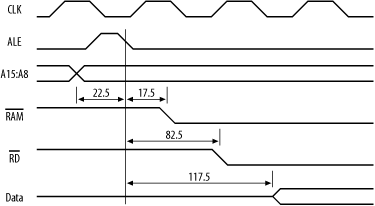
Now, an 8MHz processor expects to latch valid data during a read cycle at 147.5ns after ALE. So our SRAM will have valid data ready with 30ns to spare. So far, so good. But what about at the end of the cycle? Now, the processor expects the data bus to be released and available for the next access at 200ns after ALE falls. The RAM takes 25ns from when it is released by RD until it stops driving data onto the bus. This means that the data bus will be released by the RAM at 142.5ns. So that will work too.
The analysis for a write cycle is done in a similar manner. It is important to do this type of analysis for every device interfaced to your processor, for every type of memory cycle. It can be difficult, for datasheets are notorious for leaving information out, or presenting necessary data in a roundabout way. Working through it all can be time-consuming and frustrating, and it’s far too easy to make a mistake. However, it is very necessary. Without it, you’re relying on blind luck to make your computers go, and that’s not good engineering.
In most small-scale embedded applications, the connections between a processor and an external memory chip are straightforward. Sometimes, though, playing with the natural order of things is advantageous. This is the realm of memory management.
Memory management deals with the translation of logical addresses to
physical addresses and vice versa. A logical
address
is the address output by the processor. A physical
address
is the actual address being accessed in memory. In small computer
systems, these are often the same. In other words, no
address translation takes place, as
illustrated in Figure 6-34.

For small computer systems, this absence of memory management is satisfactory. However, in systems that are more complex, some form of memory management may become necessary. There are four cases in which this might be so:
- Physical Memory > Logical Memory
When the logical address space of the processor (determined by the number of address lines) is smaller than the actual physical memory attached to the system, the logical space of the processor must be mapped into the physical memory space of the system. This is sometimes known as
banked
memory
. This is not as strange or uncommon as it may sound. Often, it is necessary to choose a particular processor for a given attribute, yet that processor may have a limited address space: too small for the application. By implementing banked memory, the address space of the processor is expanded beyond the limitation of the logical address range.- Logical Memory > Physical Memory
When the logical address space of the processor is very large, filling this address space with physical memory is not always practical. Some space on disk may be used as virtual memory, thus making the processor appear to have more physical memory than exists within the chips. Memory management is used to identify whether a memory access is to physical memory or virtual memory and must be capable of swapping the virtual memory on disk with real memory and performing the appropriate address translation.
- Memory Protection
You may want to prevent some programs from accessing certain sections of memory. Protection can prevent a crashing program from corrupting the operating system and bringing down the computer. It is also a way of channeling all I/O access via the operating system, since protection can be used to prevent all software (save the OS) from accessing the I/O space.
- Task Isolation
In a multitasking system, tasks should not be able to corrupt each other (by stomping on each other’s memory space, for example). In addition, two separate tasks should be able to use the same logical address in memory with memory management performing the translation to separate, physical addresses.
The basic idea behind memory management is quite simple, but the implementation can be complicated, and there are nearly as many memory management techniques as there are computer systems that employ memory management.
Memory management is performed by a Memory Management Unit (MMU). The basic form of this is shown in Figure 6-35. An MMU may be a commercial chip, a custom-designed chip (or logic), or an integrated module within the processor. Most modern, fast processors incorporate MMUs on the same chip as the CPU.

In all practical memory management systems, words of memory are grouped together to form pages, and an address can be considered to consist of a page number and the number of a word within that page. The MMU translates the logical page to a physical page while the word number is left unchanged (Figure 6-36). In practice, the overall address is just a concatenation of the page number and the word number.

The logical address from the processor is divided into a page number and a word number. The page number is translated by the MMU and recombined with the word number to form the physical address presented to memory (Figure 6-37).

The simplest form of memory management is when the logical address space is smaller than the physical address space. If the system is designed so that the size of each page is equal to the logical address space, then the MMU provides the page number, thus mapping the logical address into the physical address (Figure 6-38).

The effective address space from this implementation is shown in Figure 6-39. The logical address space can be mapped (and remapped) to anywhere in the physical address space.

The system configuration for this is shown in Figure 6-40. This technique is often used in processors with 16-bit addresses (64K logical space) to give them access to larger memory spaces.

For many small systems, banked memory may be implemented simply by latching (acquiring and holding) the data bus and using this as the additional address bits for the physical memory (Figure 6-41). The latch appears in the processor’s logical space as just another I/O device. To select the appropriate bank of memory, the processor stores the bank bits to the latch, where they are held. All subsequent memory accesses in the logical address space take place within the selected bank. In this example, the processor’s address space acts as a 64K window into the larger RAM chip. As you can see, while memory management may seem complex, its actual implementation can be quite simple.

Tip
This technique has also been used in desktop systems. The old Apple /// computer came with up to 256K of memory, yet the address space of its 6502 processor was only 64K.
Figure 6-42 shows the actual wiring required for a banked memory implementation for our AT90S8515 AVR system, replacing the 32K RAM with a 512K RAM.
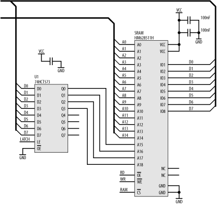
The RAM used is an HM628511H made by Hitachi. In this implementation, we still have the RAM allocated into the upper 32K of the processor’s address space as before. In other words, the upper 32K of the processor’s address space is a window into the 512K RAM. The lower 32K of the processor’s address space is used for I/O devices, as before. Address bits A0 to A14 connect to the RAM as before, and the data bus (D0 to D7) connects to the data pins (IO1 to IO8 [9]) of the SRAM.
Now, we also have a 74HCT573 latch, which is mapped into the processor’s address space, just as we did with the LED’s latch. The processor can write to this latch, and it will hold the written data on its outputs. The lower nybble of this latch is used to provide the high-order address bits for the RAM.
Let’s say the processor wants to access address 0x1C000. In binary, this is %001 1100 0000 0000 0000. The lower 15 address bits (A0 to A14) are provided directly by the processor. The remaining address bits must be latched. So, the processor first stores the byte 0x03 to the latch, and the RAM’s address pins A18, A17, A16, and A15 see %0011 (0x03), respectively. That region of the RAM is now banked to the processor’s 32K window. When the processor accesses address 0xC000, the high-order address bit (A15) from the processor is used by the address decoder to select the RAM by sending its CS input low. The remaining 15 address bits (A0 to A14) combine with the outputs of the latch to select address 0x1C000.
The NC pins are No Connection and are left unwired.
For processors with larger address spaces, the MMU can provide translation of the upper part of the address bus (Figure 6-43).

The MMU contains a translation table, which remaps the input addresses to different output addresses. To change the translation table, the processor must be able to access the MMU. (There is little point in having an MMU if the translation table is unalterable.) Some processors are specifically designed to work with an external MMU, while other processors have MMUs incorporated. However, if the processor being used was not designed for use with an MMU, it will have no special support. The processor must therefore communicate with the MMU as though it were any other peripheral device using standard read/write cycles. This means that the MMU must appear in the processor’s address space. It may seem that the simplest solution is to map the MMU into the physical address space of the system. In real terms, this is not practical. If the MMU is ever (intentionally or accidentally) mapped out of the current logical address space (i.e., the physical page on which the MMU is located is not part of the current logical address space), the MMU cannot ever be accessed again. This may also happen when the system powers up, for the contents of the MMU’s translation table may be unknown.
The solution is to decode the chip select for the MMU directly from the logical address bus of the processor. Hence, the MMU will lie at a constant address in the logical space. This removes the possibility of “losing” the MMU but introduces another problem. Since the MMU now lies directly in the logical address space, it is no longer protected from accidental tampering (by a crashing program) or illegal and deliberate tampering in a multitasking system. To solve this problem, many larger processors have two states of operation, a supervisor state and a user state with separate stack pointers for each mode. This provides a barrier between the operating system (and its privileges) and the other tasks running on the system. The state in which the processor is in is made available to the MMU through special status pins on the processor. The MMU may be modified only when the processor is in supervisor state, thereby preventing modification by user programs. The MMU uses a different logical-to-physical translation table for each state. The supervisor translation table is usually configured on system initialization, then remains unchanged. User tasks (user programs) normally run in user mode, whereas the operating system (which performs task swapping and handles I/O) runs in supervisor mode. Interrupts also place the processor in supervisor mode, so that the vector table and service routines do not have to be part of the user’s logical address space. While in user state, tasks may be denied access by the operating system to particular pages of physical memory.
[3] Datasheet nomenclature can often be very cryptic. The CL comes from clock. Since Atmel uses four character subscripts for timing references, they pad by putting CL twice. You don’t really need to know what the subscripts actually mean, you just need to know the signals they refer to and the actual numbers involved.
[4] I’m ignoring coming out of reset or just before power-off!
[5] Since we’ve covered oscillators and in-circuit programming previously, I’ll ignore those in this discussion. That doesn’t mean that you should leave them out of your design!
[6] There are actually two separate decoders in each 74HCT139 chip. We’ll only need one.
[7] Programmable Array Logic, Logic Cell Arrays, and Programmable Logic Devices, respectively.
[8] PALs may respond in 15ns or less. This is another reason why PALs are a better choice than discrete logic.
[9] Memory chip manufacturers often label data pins as IO pins, since they perform data input and output for the device.