
Architecting the last-level cache for GPUs using STT-MRAM nonvolatile memory
M.H. Samavatian1; M. Arjomand1; R. Bashizade1; H. Sarbazi-Azad1,2 1 Sharif University of Technology, Tehran, Iran
2 Institute for Research in Fundamental Sciences (IPM), Tehran, Iran
Abstract
The key to high performance on graphics processor units (GPUs) is the massive threading that helps GPUs hide memory access latency with maximum thread-level parallelism (TLP). Although, increasing the TLP and the number of cores does not result in enhanced performance because of thread contention for memory resources such as last-level cache. The future GPUs will have larger last-level cache (L2 in GPU), based on the current trends in VLSI technology and GPU architectures toward increasing the number of processing cores. Larger L2 caches inevitably have larger power consumption. In this chapter, having investigated the behavior of general-purpose GPU (GPGPU) applications, we present an efficient L2 cache architecture for GPUs based on solid transfer-torque RAM (STT-RAM) technology. Because of its high density and low power characteristics, STT-RAM technology can be utilized in GPUs where numerous cores leave a limited area for on-chip memory banks. They have, however, two important issues, high energy and latency of write operations, that have to be addressed. Low-retention time STT-RAMs can reduce the energy and delay of write operations. Nevertheless, employing STT-RAMs with low-retention time in GPUs requires a thorough study on the behavior of GPGPU applications. The STT-RAM L2 cache architecture proposed in this chapter can improve IPC by up to 171% (20%, on average), and reduce the average consumed power by 28.9% compared to a conventional L2 cache architecture with an equal on-chip area.
Keywords
GPGPU; L2 cache; Nonvolatile memory; STT-RAM; Retention time; Performance; Energy; Warp
1 Introduction
During the past decade, graphics processor units (GPUs) became one of the mainstream technologies in many-core high-performance systems. GPU architecture is a type of single-instruction multiple-thread (SIMT) architecture, which tries to achieve massive thread-level parallelism (TLP) and improve the throughput. These characteristics led to the growing interest in general-purpose GPUs (GPGPUs). The main factor in this SIMT architecture is to keep the entire processor active and decrease the idle cycles by minimizing or covering stall cycles of threads. GPUs form logical groups of parallel threads belonging to the same instruction pack, named warps (or wavefront in AMD terminology) and schedule a number of them for interleaved execution on an SIMT core. This can lead to higher memory performance and reduce the problem of branch divergence. A large body of recent works [1–6] focused on this issue. Although these works diminish idle cycles by switching threads on stall times based on their proposed scheduling algorithms, high latency of main memory in GPUs causes significant idle times when all threads are stalled and no other threads exist for execution. On-chip memories play a substantial role in decreasing stall cycles of threads on memory accesses. Therefore, cache memories in GPU architectures become a critical issue due to the limited on-chip area available for them in GPUs.
In the same way, recent trends in GPU architecture show designers’ interest in assigning most of the chip area to more compute cores rather than on-chip memories. Consequently, for supporting more thread executions in GPUs, besides compute cores, register file have priority to be placed on chip. While warp size is rather fixed through successive GPU generations (due to the overhead of branch divergence for larger warps [1]), the number of warps assigned to one SIMT core have been steadily increasing in recent products (e.g., 64 warps per SIMT core in Kepler [7] compared to 24 in G80 [8]).
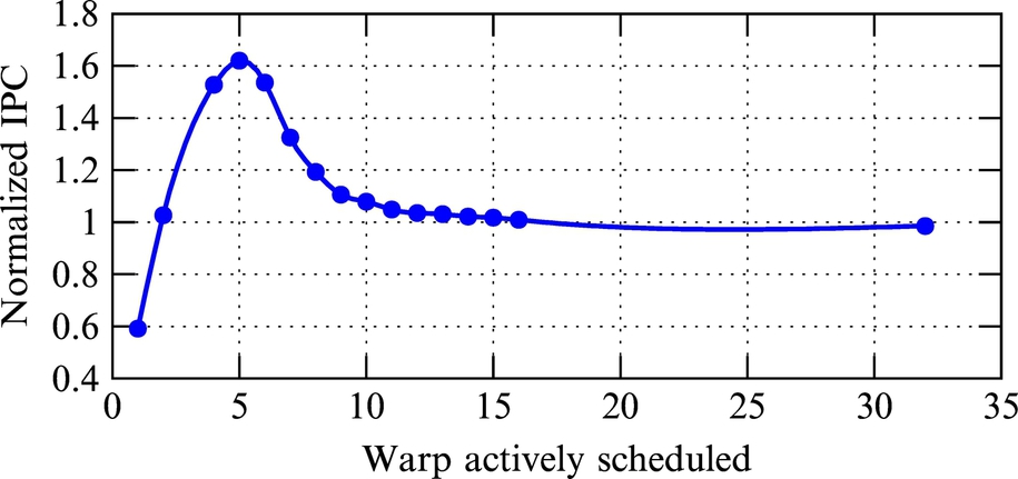
Scheduling more warps improves utilization and throughput of the GPU and can better cover access latency of the main memory. On the other hand, increasing the number of scheduled warps will increase the accesses to the L1 data cache. The emerging problem is that when a new warp is issued for execution, it may cause new accesses to the L1 data cache that cause prior scheduled warps data to be sent out, which is known as cache Thrashing. This phenomenon is made more tangible when studies on GPU cache hierarchy reveal that most L1 data cache hits result from intrawarp locality [2] rather than interwarp locality. The probability of cache Thrashing increases when the number of actively scheduled warps increases. Although increasing the number of active threads will improve throughput and core utilization, cache Thrashing is an aftereffect that degrades the performance of GPU. Hence, as Fig. 1 highlights, for a fixed L1 cache size of 32 KB, the gained performance is maximized when a specific number of warps are assigned to each SIMT core, that is, less or more warps than such a specific number will result in lower performance. Additionally, increasing the number of warps necessitates a larger L1 cache to sustain performance. Designers are also constrained from increasing L1 cache size for two reasons: first, the SIMT core is more dedicated to compute cores and register files than to memories (as previously mentioned); second, increasing intra-SIMT core memory size increases the access latency of the cache due to the larger data array and the cache controller. Higher access latency penalizes performance as a consequence.
With the constant L1 cache size and the growing number of warps scheduled per SIMT core, there are more access misses in the L1 cache, which results in more access traffic pressure being put on the L2 cache as the next level cache. If the L2 cache cannot handle the amount of accesses, the next memory in the memory hierarchy is accessed. In GPUs, the next memory hierarchy is the main memory with large gap in access latency toward L2 and L1 caches. Accesses to the lowest level cause a long stall time. Thus the L2 cache size has to be increased in order to prevent long latency access to the main memory. Also, despite L1 caches, the L2 cache access latency is not so critical; however, the on-chip memory area remains a concern. The trend in recent GPU architectures also confirms the approach of increasing L2 cache size (e.g., L2 cache size increased from 786 KB in Fermi to 1536 KB in Kepler, both having a maximum of 48 KB L1 D-cache). In recent GPUs, the SRAM L2 cache size kept pace with this capacity demand. With current chips, maximum power budget being used, a further increase in the number of warps (requiring further growth of L2 cache size) will be very difficult. This is also true for increasing the number of cores in future GPUs.
Entering a deep nanometer technology era where leakage currently increases by 10 times per technology node, SRAM arrays confront serious scalability and power limitations [9]. Promising types of nonvolatile memories are now being introduced. Phase change memory (PCM), magnetic-RAM (MRAM), solid transfer-torque RAM (STT-RAM), racetrack memory, and resistive RAM (ReRAM) [10–14, 67] are among the most popular nonvolatile memories. These memories have different specifications and characteristics, and based on that, each of these memories fit better than any of volatile memories. Density, low leakage power, and scalability are the most important advantages of nonvolatile memories over typical volatile memories such as SRAM and DRAM. Among the known technologies to replace SRAM is spin torque transfer RAM (STT-RAM) [15]. The STT-RAM cell has near-zero leakage power and is about 4× denser than the SRAM cell. The promising characteristics of STT-RAM (especially its higher density and lower power consumption) make it a good candidate for building L2 caches of future GPUs. Nevertheless, writing to an STT-RAM cell requires the use of a large amount current for a long period of time. So, the realization of such a promising nonvolatile memory structure will face problems regarding latency and energy of memory accesses.
Several proposals, at both a circuit and an architectural levels [16–19], have been made to address the energy and latency challenges of STT-RAM writes. Another approach for mitigating the write problem of STT-RAM cells is device-level optimizations. Reducing the retention time of STT-RAM cells is one of the most effective optimizations; it was introduced in different works such as [20, 21]. Reducing the retention time can further reduce write accesses latency and energy in STT-RAM drastically. On the other hand, reduction of STT-RAM cells requires accurate optimization based on observing applications on the targeted hardware platform.
Analyses for a wide range of GPGPU applications show a large variation in the intensity of writes to different blocks of the L2 cache. Some cache blocks get write access more than other cache blocks, and the distribution of write accesses are uneven between different blocks. For simplicity, we define write working set (WWS) as a data set that gets write access during an application’s runtime. Based on observations in this chapter, WWS of the L2 cache has two specific features: the WWS of typical applications within a short period is small, and the rewrite interval (RI) time of the blocks in WWS is usually short (lower than 100 μs). Thus we refer to this portion of WWS as temporary WWS (TWWS). Consequently, a 10-year data retention in STT-RAM is not required for most of the blocks in WWS. These features give us the opportunity for device-level optimization for GPU cache as it has also been shown that physical and magnetization properties of an STT-RAM cell are a trade-off between device nonvolatility and latency/energy of write operations [20].
In this chapter, we propose an STT-RAM L2 cache architecture with two parts: a small-sized low-retention array (LR) optimized for write operations and a large-sized high-retention array (HR). LR cache is responsible for holding TWWS of the applications. HR cache, on the other hand, provides a high-capacity array, holding a large portion of L1 thrashed data that are mostly intended to be read-only or in frequently written. To increase the STT-RAM cache efficiency, the proposed architecture has three key differences from the traditional on-chip GPU caches: (1) A monitoring logic determines write-intensive data blocks forming TWWS of the running applications. The main features of this module are its low overhead and fast reaction to the changes in WWS. Furthermore, the monitoring logic adaptively monitors workload behavior in the runtime. Based on the monitored behavior, a decision is made in order to minimize the number of writes on HR, alongside minimizing the overhead of writes in proportion to the baseline; (2) the cache search mechanism is modified for better energy efficiency based on access types and data types that are more likely to be present in LR and HR; and (3) the cache eviction policy is changed slightly in order to keep more rewritten data blocks in LR and gain better energy efficiency. We use a simple buffer to take care of data expiration in LR based on the elapsed time of the data rewrites and postpone the refreshing of cache blocks until the last cycles of the retention period.
In the following section, we present a brief background on the baseline GPU architecture and its memory hierarchy. In addition to GPU architecture, STT-RAM concepts are briefly explained. Section 3 identifies previous related work on GPU memory hierarchy, STT-RAMs, and more details on employing STT-RAM in GPU architectures. The proposed architecture, from motivation to design, is presented in Sections 4 and 5. In Section 6, details of our implementation and its overhead are discussed. Section 7 presents evaluation results, and finally, Section 8 concludes the chapter.
2 Background
2.1 GPU and Its Memory Hierarchy
A GPU comprises multiple stream multiprocessors (SMs), called compute units in AMD architectures, each consisting of a rich memory hierarchy including register files, shared memory, cache arrays, and a number of simple cores called stream processor (SP). Generally, SMs are known as SIMT cores. GPUs use SMs as vector processors to achieve TLP by executing single instruction over multiple threads. A GPU application comprises one or more kernels. Each kernel launches a hierarchy of threads on GPU. Hundreds of threads create a grid composed of cooperative thread arrays (CTAs) or thread-blocks (TBs). The CTAs are allocated to SMs as single units of work. TBs decompose to groups of 32 threads for execution on an SM. These groups of threads are called warp in NVIDIA and wavefront in AMD terminologies, respectively. In other words, warps are the smallest fetched units within this hierarchy.
Each thread can access different data types that are annotated in GPGPU programming with separated address ranges in the main memory. These data types comprise global, local, texture, and constant data. A thread commonly accesses these data types through a rich memory hierarchy, as shown in Fig. 2B. The local data is usually placed in a dense register file array that is private to each SM. Global data refer to the data shared among all threads within a grid.
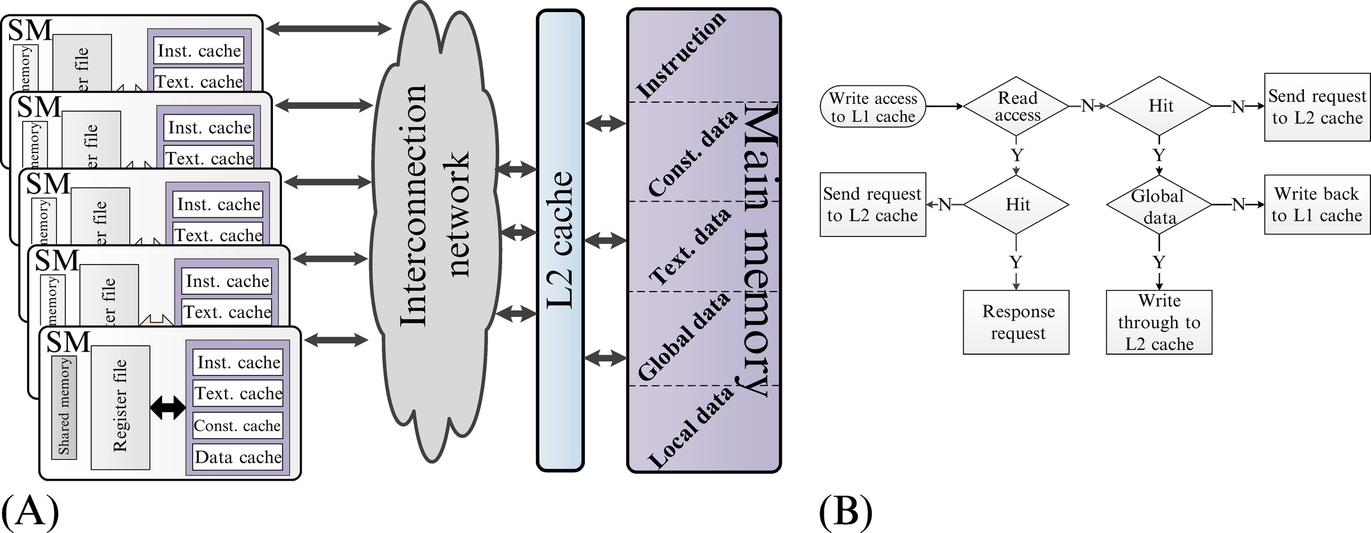
When a thread requests data from the off-chip main memory, the accesses pass through a two-level cache hierarchy. Each data type is placed in its specific cache memory in the first level of memory hierarchy. Local and global data are placed in D-caches while texture and constant data are placed in texture and constant caches, respectively. Instructions are placed in instruction caches. Additionally, unlike D-cache, which is a read-write cache memory, instruction, texture and constant caches are read-only caches. Each SM is also associated with a software-managed local memory for shared data accesses by threads within a TB. Note that shared data are not in this memory hierarchy and are directly placed in the shared memory. Shared memory is not the concern in this study; however, interested readers can refer to [22–25] for more details.
The existence of different data types and caches in GPU brings up different policies for read and write accesses. The L1 caches are private to SMs with no coherency among them because there is no data communication between SMs. Because L1 caches are not coherent, all write operations of global data are handled as write-evicts (on hit) or write-no-allocates (on miss). Local data are written into the associated L1 cache with a write-back mechanism (Fig. 2A). The L2 cache is a banked cache array shared by all SMs and backs all types of data. Each L2 bank communicates with L1 caches of different cores through an interconnection network. L2 cache uses write-back policy with respect to the main memory. At the highest level of hierarchy, each L2 bank has a point-to-point connection with a dedicated off-chip memory controller. A more complete description of GPU memory system is available in Ref. [26].
The L1 data cache and shared memory in NVIDIA Fermi GPUs are uniform memory in each SM with the ability of reconfiguration and have a fixed total (L1 + shared memory) capacity of 64 KB per SM. L1 data cache and shared memory can be configured as (16 KB + 48 KB) and (48 KB + 16 KB). This gives flexibility to programmers to set cache and shared memory sizes based on the requirements of nonshared and shared data, respectively. In the new Kepler GK100 (32 KB + 32 KB), configuration is implemented, too. Moreover, texture and constant caches are unified as read-only data cache in the Kepler architecture. In the new NVIDIA Maxwell GM204 architecture, a fixed 64 KB dedicated shared memory is made possible by combining the functionality of the L1 and texture caches into a single unit [27].
2.2 Nonvolatile Memories
In this section, we briefly overview ReRAM, STT-RAM, and racetrack memory technologies because, among nonvolatile memories, they have features closer to SRAM. More detailed description can be found in Refs. [13, 14, 28]. Then we will focus on STT-RAM based on its capability of reducing retention in order to overcome one of its main challenges and and make its read latency comparable to SRAM’s.
The ReRAM memory element consists of one inert electrode at the top (e.g., platinum), an electrochemically active electrode at the bottom (e.g., copper), and the oxide layer between inert and active electrodes. When a positive bias is applied to the active electrode, the metal ions are forced to migrate through the oxide and eventually reach the electrode on the other side (inert electrode). The ion path is highly conductive, and the cells, equivalent resistance value is low (1). The low-resistance state can be changed again to a high-resistance state by positively biasing the inert electrode (0). The biggest advantage of the ReRAM technology is the high compatibility with CMOS processes, which means that it can be fabricated at the same die that processor and SRAM caches are fabricated. Furthermore, the voltage required for ion path-forming process proportionally relates to the oxide layer thickness. These advantages gives ReRAM a strong cost-competitive advantage over SRAM. However, its low cell endurance (up to ∼1011 writes [29]) and high access latency limits its use at near-processor cache levels.
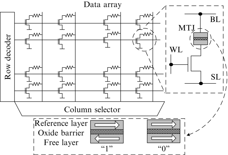
STT-RAM technology is a type of scalable MRAM. The basic structure of an STT-RAM cell is composed of a standard NMOS access transistor and a magnetic tunnel junction (MTJ) as the information carrier (Fig. 3). MTJ consists of two ferromagnetic layers and one oxide barrier layer in between (Fig. 3). One of the ferromagnetic layers (i.e., the reference layer) has a fixed magnetic direction while the magnetic direction of the other layer (i.e., the free layer) can be changed by directly passing a spin-polarized current. If these two layers are magnetized in antiparallel (parallel) directions, the MTJ resistance is high (low), indicating bit “1” (“0”). STT-RAM has a limited write endurance per cell (up to ∼ 1012 writes [30]), and when the number of writes to a cell reach its maximum limit, the cell may lose its ability to change the magnetization status of the free layer, thus creating data errors.
Racetrack memory, also known as domain wall memory (DWM), is a spin-based memory technology, which represents information using the spin orientation of the magnetic domains in a ferromagnetic wire, as shown in Fig. 4A. Each of these domains can independently take any magnetic orientation (up-spin or down-spin). Therefore multiple bits of data can be packed into a single DWM device, resulting in very high density. Three basic operations can be performed on a DWM device: read, shift, and write. The MTJ structure, shown in Fig. 4A, is used to read data from the DWM device similar to STT-RAM. In a DWM device, all the magnetic domains in the ferromagnetic wire share a single MTJ. The bit to be read/written needs to be aligned with the MTJ before it can be accessed. This is accomplished using a property that is unique to DWM, called domain wall motion, which refers to the shifting of magnetic orientations of domains in the ferromagnetic wire. When a current pulse of a suitable magnitude is applied through the ferromagnetic wire, the magnetic orientation of each domain is shifted in a direction opposite the direction of current. Additional domains are provided in the device to prevent loss of data at the extrema while shifting.
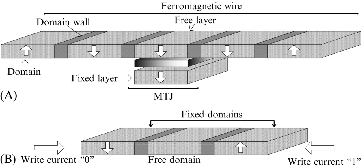
Formerly, the write operation was also performed with the MTJ similar to STT-RAM. This write operation is highly energy-consuming. However, a recent development in DWM has eliminated this inefficiency. It has been experimentally shown that domain wall motion (originally intended to realize shifts) can also be used to perform fast, energy-efficient writes in DWMs. This operation, often referred to as shift-based writes, is demonstrated in Fig. 4B. The structure of the write operation consists of a ferromagnetic wire with three domains: two fixed domains and a free domain. The magnetization of the two fixed domains are hard-wired to up-spin and down-spin during fabrication. However, the magnetization of the free domain, which is sandwiched between the fixed domains, can be varied by shifting the magnetization of one of the fixed domains by applying a current pulse in the appropriate direction.
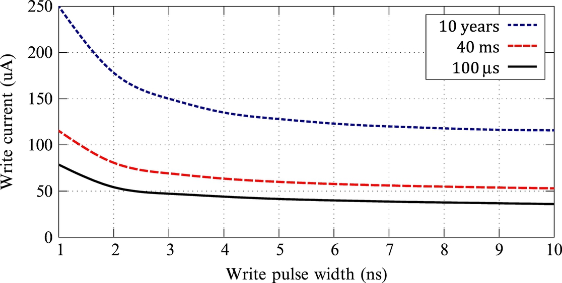
The main challenge of racetrack memory is the access latency to data stored in a DWM tape that is variable depending on the number of shifts required. Varying the number of bits stored in each DWM tape brings a unique trade-off between density (which increases with more bits-per-tape) and average access latency. On the other hand, there is another mechanism to decrease the write operation problems in MTJ cells. Reducing the MTJ cell retention time results in decreasing write operation energy, in addition to reducing cell reliability. In other words, there is a trade-off between data retention and write energy in MTJ cells. Reduction of the write time period results in more current; therefore, for faster write operations, a higher amount of current and more power is needed. Due to the constraint on maximum current in chips, the write pulse period must be increased in order for the write current to be decreased. By reducing the retention time, the level of write current decreases for different write pulses, so shorter write time becomes possible. Fig. 5 shows different write currents as a function of the width of write pulses for 10 years, 40 ms, and 100 μs retention times. More details on STT-RAM and the model used in this chapter can be found in Ref. [21].
3 Related Work
In this section, we briefly review the recent research in GPU memory hierarchy and architectures exploiting STT-RAM, and we focus on the most important studies alleviating cache hierarchy shortcomings in GPU by using STT-RAM.
GPU memory hierarchy
Many researchers have considered the memory hierarchy of GPUs to reduce access latency of the memory [31], improve memory access coalescing [23], and increase the parallelism among memory controllers [32]. DRAM scheduling [33] and prefetching [34] techniques have also been introduced for GPUs. In addition, a number of recent works concentrate on the GPU cache from various perspectives.
Jia et al. [35] specified the memory access patterns in GPUs. Based on such information, the suggested algorithm estimates how much of the bandwidth is required when cache memory is on/off and then decides which instruction data is placed in the cache. In Ref. [36], Tarjan et al. tried to quickly cross the interconnection network to access L2 by handling L1 misses using the copies kept at other L1 caches in other SMs. To do so, they used a sharing tracker to identify whether a missed data block in L1 cache is present in other L1 caches. Rogers et al. [2] presented a method called Cache-Conscious Wavefront that employs a hardware unit to examine intrawarp locality loss when a warp is selected for fetching. Hence, their mechanism prevents the issuing of new warps that might result in thrashing previously scheduled warps, data in the cache. Similarly, in Refs. [37–39], the same problem is tackled by modifying the cache indexing function, warp throttling, and detecting critical warps in order to maintain useful data in the cache. Gebhart et al. [40] designed a uniform memory that can be configured to be register file, cache, or shared memory regarding the requirements of the running application. Moreover some other works, such as [41, 42], tried to reduce the power consumption of GPU by observing and considering GPU memory hierarchy from the main memory to the register file.
STT-RAM
Dong et al. [15] investigated the possibility of replacing SRAM with MRAM by introducing a model for power, area, and performance of MRAMs, which is used in our power and performance calculations, too. As the main STT-RAM challenges are the write operation’s latency and energy, most of the research focused on these aspects of STT-RAM. Rasquinha et al. [19] proposed an energy-efficient cache design in order to decrease STT-RAM dynamic energy by managing operations on cache. Zhou et al. [18] introduced the early write termination (EWT) technique to prevent writing unchanged data bits. Some other researches such as Refs. [16, 17] used a combination of MRAM and SRAM to overcome disadvantages of both technologies and use their advantages. On the other hand, Smullen et al. [20] considered, the relaxing nonvolatility of speed and energy-efficient STT-RAMs. Sun et al. [21] used STT-RAM cells with different retention times; they used a single low-retention STT-RAM L1 cache. For higher level caches, a two-retention STT-RAM structure was used, where data blocks with frequent writes are migrated to the cache blocks with low-retention time. In Refs. [43, 44], different refreshing mechanisms are proposed to efficiently employ low-retention STT-RAM.
In Ref. [45], a two-part main memory consisting of a small DRAM part and a large PCM part is presented. In contrast to our proposal, DRAM and PCM parts are managed in a hierarchical manner, that is, DRAM works as a cache for the large PCM memory. Additionally, the differences between the features of the cache and main memory make this approach inapplicable for designing a cache. For instance, in Ref. [45], the writes are forwarded to the PCM part instead of DRAM, because it is assumed that the locality of the data evicted from the cache was already exploited. However, in the cache, due to the existence of data locality, there could be multiple writes on a block, so it is better to forward those to the write-friendly part.
GPU memory and STT-RAM
Recent work [46, 47] used the nonvolatile DWM in both register files and the cache memory of GPUs. Also, Refs. [48–50] used STT-RAM in GPU register file with different approaches such as hybrid memory, write awareness, and multilevel cell design, respectively. Al-Maashri et al. [51] focused on using STT-RAM technology for 3D stacking of texture memory. They did not really address the use of GPUs for general-purpose high-performance computing but considered graphics applications. In research by Goswami et al. [52], a single and uniform low-retention time STT-RAM was used for the register file and constant and texture caches, and a hybrid memory (STT-RAM and SRAM) was employed for the shared memory of GPGPUs. To remedy the high-energy consumption of write operations, the EWT mechanism [18] with a higher granularity was used. Also, an SRAM write-back buffer was used to coalesce write operations of different threads to the STT-RAM register file.
Because L1 cache latency is critical to the overall application performance, in this chapter, we concentrate on studying trade-offs between STT-RAM retention time and write latency/energy and propose an architecture to surpass the cache shortcomings using this promising technology in GPU’s last-level cache (LLC). The L2 cache is typically a unified large cache (e.g., 1.5 MB in Nvidia’s GK110 and 2 MB in Nvidia’s GM107), which is greater than the total L1 caches in terms of size. Additionally, L2 cache is responsible for improving the effective memory access bandwidth of the SMs by reducing the number of off-chip memory accesses. Typically, the latency of L2 cache accesses is hidden by switching between multiple warps that are active in the SMs. Therefore implementing L2 cache using STT-RAM technology seems more reasonable and effective in GPUs.
4 Two-Part L2 Cache Architecture
4.1 Motivation
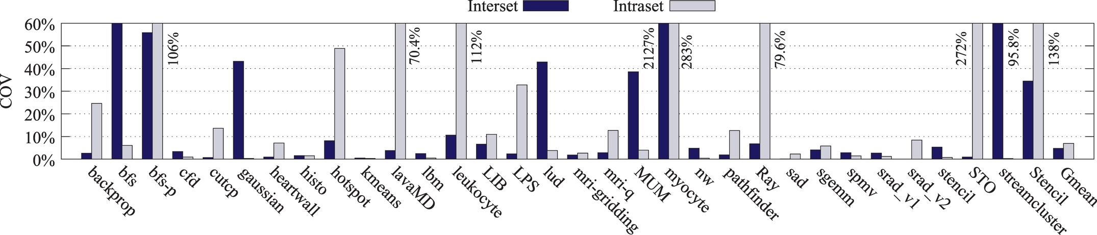
GPGPU applications perform different write patterns on cache blocks. In Ref. [53], the coefficient of variation (COV) parameter was used to indicate inter and intracache set write variations in chip multiprocessor (CMP) applications. Fig. 6 shows inter and intracache set writes COV for GPGPU workloads. Applications such as bfs, bfs-p, lavaMD, leukocyte, RAY, STO, streamcluster, and stencil have more writes on fewer cache blocks, whereas other applications have more balanced writes over L2 blocks. This justifies using an STT-RAM region having a reduced retention time that favors write operations. Ideally, we expect this region to hold data blocks with high rewrite frequency in order to minimize write energy and improve the cache performance.
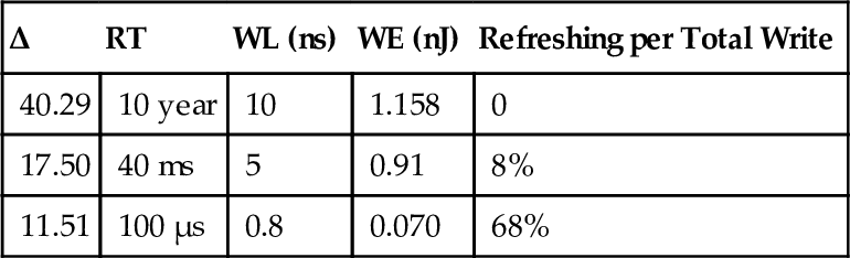
Reducing the retention time of STT-RAM cells increases the error rate because of early data bit collapse (with respect to high-retention cells). Table 1 shows different magnetization stability heights (△) and their corresponding retention times (RT), write operation energies (WE), and latencies (WL). The 10-year retention time STT-RAM cell has the most write energy and latency with no error rate because of its high data stability. Any reduction in the retention time of STT-RAM cells from this baseline reduces write operation energy and latency due to the reduction in the current needed for writing, but more refreshes are required to prevent data loss. This leads us to using a nonuniform STT-RAM cache structure with different retention times.
Table 1
STT-RAM Parameters for Different Data Retention Times
| Δ | RT | WL (ns) | WE (nJ) | Refreshing per Total Write |
| 40.29 | 10 year | 10 | 1.158 | 0 |
| 17.50 | 40 ms | 5 | 0.91 | 8% |
| 11.51 | 100 μs | 0.8 | 0.070 | 68% |
Utilizing low-retention STT-RAM is meaningful when it can hold WWS of an application to minimize the write energy. Also, refreshing overhead of cache blocks in low-retention part of the cache must be reasonable.
As mentioned before, the WWS of most GPGPU applications is small and within short periods of time. Fig. 7 schematically shows spatial and temporal distribution of write accesses to the LLC. At each TWWS (t1 and t2 in Fig. 7![]() ), a number of data blocks are accessed for write, and then there are no significant write accesses to the LLC for a while (t1′ and t2′ in Fig. 7
), a number of data blocks are accessed for write, and then there are no significant write accesses to the LLC for a while (t1′ and t2′ in Fig. 7![]() ). In a TWWS, each data block may be accessed one or more times. We define write-to-write time (W2W) as the time difference of two successive accesses to a block and use it indirectly to estimate the average TWWS duration for each workload. For this purpose, in the first phase, we count data blocks with W2W greater than a specific time range (time range 1 in Fig. 7
). In a TWWS, each data block may be accessed one or more times. We define write-to-write time (W2W) as the time difference of two successive accesses to a block and use it indirectly to estimate the average TWWS duration for each workload. For this purpose, in the first phase, we count data blocks with W2W greater than a specific time range (time range 1 in Fig. 7![]() ). Then we increase the time range (time ranges 2, 3, …, n in Fig. 7
). Then we increase the time range (time ranges 2, 3, …, n in Fig. 7![]() ) and again count data blocks with W2W greater than each of the time ranges. This is repeated until a time range is found such that the number of data blocks with W2W greater than that remains almost unchanged (Time ranges 3, 4, …, n in Fig. 7
) and again count data blocks with W2W greater than each of the time ranges. This is repeated until a time range is found such that the number of data blocks with W2W greater than that remains almost unchanged (Time ranges 3, 4, …, n in Fig. 7![]() ). This range marks the end point for each workload and is an approximation for the time difference between the beginning of two consecutive TWWSs (t1 + t1′ in Fig. 7
). This range marks the end point for each workload and is an approximation for the time difference between the beginning of two consecutive TWWSs (t1 + t1′ in Fig. 7![]() ).
).
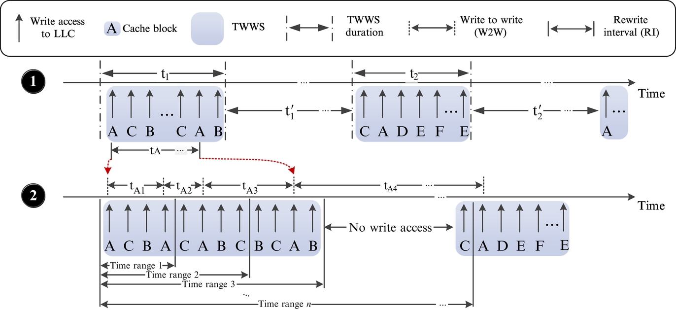
Afterward, to determine the length of TWWS, we observe the distribution of RI, the time difference between first and last accesses to a block in TWWS, for example, tA in Fig. 7![]() . Wehave chosen RI as a representative for TWWS duration, since a decline in accesses to most of the blocks constituting TWWS is observed in a short period of time. Therefore the time range that has the most RI distribution in it is probably the TWWS duration. For each workload, the TWWS duration is calculated based on this method. Table 2 shows the estimated TWWS durations in cycles.
. Wehave chosen RI as a representative for TWWS duration, since a decline in accesses to most of the blocks constituting TWWS is observed in a short period of time. Therefore the time range that has the most RI distribution in it is probably the TWWS duration. For each workload, the TWWS duration is calculated based on this method. Table 2 shows the estimated TWWS durations in cycles.
Table 2
TWWS Features for Different Workloads
| Workloads | Est. TWWS Dur.a (Cycle) | WWS Size (No. of Blocks) | Avg. No. of Acc. per Blockb | Workloads | Est. TWWS Dur. (Cycle) | WWS Size (No. of Blocks) | Avg. No. of Acc. per Block |
| backprop* | 400 | 341 | 232 | bfs-p* | 1100 | 202 | 64 |
| bfs | 1000 | 284 | 356 | cfd* | 2500 | 206 | 117 |
| cutcp | 100 | 16 | 32 | gaussian | 400 | 267 | 70 |
| heartwall* | 4200 | 776 | 70 | histo* | 500 | 338 | 209 |
| hotspot* | 900 | 79 | 128 | kmeaans | 2200 | 46 | 26 |
| lavaMD | 200 | 297 | 313 | lbm* | 600 | 235 | 201 |
| leukocyte* | 1900 | 314 | 14 | LIB | 100 | 251 | 2 |
| LPS | 500 | 144 | 200 | lud | 400 | 237 | 79 |
| mri-gridding* | 1200 | 415 | 327 | mri-q | 2300 | 81 | 7 |
| MUM* | 100 | 222 | 2 | myocyte | 300 | 1 | 2 |
| nw | 600 | 201 | 142 | pathfinder | 500 | 52 | 74 |
| RAY* | 100 | 467 | 2 | sad | 4400 | 408 | 354 |
| sgemm | 2300 | 107 | 40 | spmv | 200 | 65 | 45 |
| srad-v1 | 2800 | 295 | 59 | srad-v2 | 700 | 451 | 416 |
| stencil | 300 | 297 | 215 | STO | 300 | 89 | 16 |
| streamcluster | 2600 | 26 | 9 | Avg. | 1177 | 232 | 100 |
a Estimated TWWS duration.
b Average number of accesses per block.
* Register file limitation is bottleneck for TLP.
Finally, Fig. 8 shows the distribution of data blocks whose RIs are in the estimated TWWS duration. More than 80% of rewrite accesses to the data blocks are under each workload’s estimated TWWS duration, which proves our estimation accuracy. Moreover, this justifies the assumption that we have short-time periods in GPGPU applications with burst write accesses to a specific number of blocks in L2 cache. Additionally, Table 2 shows the maximum number of distinct cache blocks accessed in the TWWS duration for each workload. With respect to the average of maximum TWWS sizes, a small write-optimized part of the cache is needed for containing the TWWS of workloads. Moreover, a large high-retention part of the cache is used to hold read-only and less frequently written data blocks.
4.2 The Proposed Two-Part Cache Architecture
In this section, we describe our proposed STT-RAM L2 architecture for replacing SRAM L2 in GPUs. Because it was justified in the previous section, we need to have two parallel low-retention and high-retention parts (LR and HR) to keep more frequently and less frequently written blocks, respectively. Therefore, we propose a two-part L2 cache with different data retention times to manage write operation energy and data refreshing problems by migrating more frequently written data blocks from HR to LR, and vice versa. Fig. 9 depicts the block diagram of the proposed STT-RAM L2 cache architecture. Two parallel structures with different data retention times, swap buffers between themselves, and counters and some hardware logic for managing search in and migration between two cache parts are employed. Our L2 cache architecture has three main characteristics that make it distinct from typical GPU L2 caches, which are explained next.
Monitoring mechanism
The first characteristic is a monitoring logic for determining whether a data block is frequently written. Write counter (WC), a simple monitoring logic, is the counter responsible for this job. The WC of each cache line is incremented whenever a rewrite access is performed on that cache line. When the WC exceeds the threshold, its corresponding data block is detected as part of the TWWS, and then it will be migrated to LR. As HR is banked, a HR-to-LR buffer is necessary for data migration. Moreover, the write latency gap between HR and LR may cause problems when a block leaves LR part. So a small buffer is needed to support data block migration from LR to HR, too. Regulating write threshold (WT) value (i.e., a threshold based on which a decision is made regarding the migration of a block) is done by a dynamic mechanism during runtime by the dynamic threshold regulator (DTR), which is explained in the next section.
Search mechanism
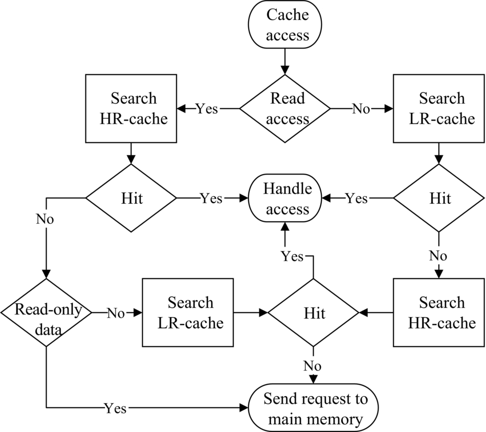
The second difference is the search mechanism among two cache parts. Because we have two parallel cache arrays, different approaches can be considered in order to handle cache accesses. Two possible approaches include parallel and sequential searches in LR and HR. Searching in LR and HR in parallel results in better performance, but is more power-consuming. In contrast, sequential search may cause more latency, but saves power.
Fig. 10 shows the timing for both search mechanisms on different scenarios. Sequential search mechanism adds an extra cycle when the first cache selected for searching does not hold the requested data block (Fig. 10A and C). However, the overhead of searching both LR and HR tag arrays can be avoided if the requested block is found in the first part (Fig. 10B and D). In order to address the shortcomings of each of the parallel and sequential search mechanisms, the data and access type aware cache search mechanism (DAACS), shown in Fig. 9, is employed.
The DAACS determines which part of the L2 cache must be searched first, regarding the access types (read or write) and data types (instruction, texture, constant, global or local data). If the requested data is not found in the first cache part, the second cache part will be searched. Obviously, as frequently written data are kept in LR, it is searched first for a write request. For read accesses, on the contrary, the HR part is searched first. Moreover, read-only data (i.e., texture and constant data and instructions) are never migrated to the LR part. Thus only the HR will be searched upon receiving access to these data types, regardless of whether the data exists in HR or not. Fig. 11 shows a flow diagram of the DAACS.
Eviction policy
The third difference is the eviction policy in our two-part cache. Inevitably, a short time after the migration of data blocks to LR, the small LR array will be fully utilized. Then, after each migration from HR to LR, a data block eviction is probable in both HR and LR. Clearly, a data block should be evicted from the LR cache when a new data block is migrated from HR to LR. If the evicted data block from LR returns to HR, it may cause an eviction from HR, too.
First, LR replacement policy is chosen to be write-LRU. Write-LRU is only sensitive to write accesses and read accesses does not change the LRU state. Because LR is the memory in which TWWS is placed, write-LRU helps to maintain data blocks on which more write operations are performed, rather than read operations. Second, when a data block is evicted from LR, two approaches are taken: the evicted data block is forced to be written back to the main memory (blocks in LR part are always dirty), or the evicted data block from LR is migrated to HR. The first approach causes traffic overhead in the main memory, but the second one, depending on the reserved place for the evicted LR data block in HR, may not impose a write-back to the main memory. The worst case occurs when the evicted data block from HR is also dirty, thus it additionally costs one read from HR and one write to the main memory. To minimize the overhead, we can take one of the two approaches dynamically based on LRU status of HR. This means that, if the LRU block in HR is dirty, then the LR’s evicted block is written back to the main memory; otherwise, the evicted block is migrated to HR.
Refreshing mechanism
Because the retention time of the cache parts are reduced to favor write operations on STT-RAM cells, data refreshing is a new issue that needs to be addressed. Error prevention [54–56] or data recovery [57] are the common solutions, but they are not applicable here because of numerous bit collapses when a cache line with low-retention time expires. A simple mechanism based on Ref. [43] can be used to handle retention time expiration. In Ref. [43], a counter is used per cache line to keep track of the lifetime of the cache block. Similar to Ref. [43], in this work, we employ such a counter, retention counter (RC), with different policies. With respect to the value of RC, we can opt to refresh or invalidate the cache block, or perform a write-back to the data block. Our architecture uses all three approaches appropriately. If an RC saturates, this means that its corresponding cache block retention time has expired. Therefore the cache block will be invalidated. Note that before RC saturates (i.e., one cycle before counter saturation), the proper decision must be taken.
Fig. 12A shows that the RI distribution in LR. The 100 μs is a reasonable retention time due to its low write latency/energy and low overhead of refreshing. Most of the workloads have RIs lower than 100 μs. In order to refresh a cache block, it is read and pushed into a buffer and then rewritten in the cache to prevent data loss. The LR-to-HR buffer is used for refreshing cache blocks in LR. Because the LR-to-HR buffer is also used for data block migration between LR and HR, by using a tag in this buffer, the blocks migrating to HR and those needing to be refreshed are differentiated. When the LR-to-HR buffer is full, the cache block that needs refreshing is forced to be written back to the main memory before its retention time expires. Fig. 12B shows RIs for cache blocks in HR. We can draw two deductions from Fig. 12B. First, a 10-year retention time for HR is not needed, and 40-ms retention time covers the lifetime of more than 97% of cache blocks in HR. We can invalidate the few remaining cache blocks (i.e., less than 3%) with higher lifetimes and force them to be written back if they are dirty.
5 Dynamic Write Threshold Detection Mechanism
5.1 Motivation
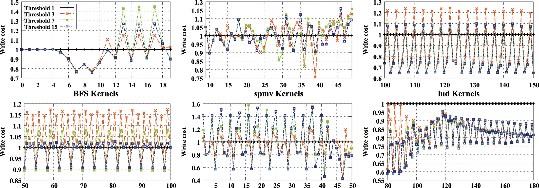
It is important to minimize the number of block transfers between HR and LR to reduce the overall write overhead with respect to the baseline architecture. Low WTs cause a high number of swaps between HR and LR and, consequently, increase the dynamic power. As dynamic power of STT-RAM memory is intrinsically more than that of SRAM, it is a critical factor for utilizing STT-RAM in our design. On the other hand, if WT is high, a lower number of blocks are migrated from HR to LR. As a result, more writes are performed on HR, and more dynamic power is consumed because of higher dynamic power of write operations in HR, whereas LR is left underutilized. This means that the effective size of cache decreases, which may cause performance degradation. Because of the different types of workloads on GPGPU regarding memory intensity and variation in the number of write operations, having a fixed threshold is not efficient. Fig. 13 shows the write cost in our two-part cache for different WTs. During various phases of runtime of an application, minimum write cost may be caused by different WTs. On the other hand, appropriate WTs may differ from one application to another. We design a dynamic architecture to regulate WT in the runtime based on the write costs of LR and HR, along with the number of block swaps between them.
5.2 Threshold Analysis
For designing an adaptive monitoring logic, we need to determine the parameters affecting cache write cost, and the affect of WT on these parameters. Eq. (1) indicates that the total cache write cost (TWCost) is composed of write costs of HR (WCostHR) and LR (WCostLR), each calculated by the multiplication of its write cost per block (WCB) and write rate (Eqs. 2, 3).
WHR is the summation of write hits (WHitHR), misses, and swaps (Eq. 4). The same parameters, excluding misses, form WLR (Eq. 5). Misses are excluded from WLR, because the missed data blocks are written in HR first.
On the other hand, WCBHR can be calculated as the product of WCBLR and a constant factor (Eq. 6).
Therefore TWCost can be calculated as:
Thus Miss, Swap, WHitHR, and WHitLR are the factors that must be considered in regulating WT. Our observations show that the effect of WT changes on miss rate is less than 0.13%. Thus they can be ignored as an affecting parameter for the sake of simplicity. Table 3 explains the effects of the other three parameters on WT.
Table 3
Effects of Write Cost Parameters on WT
| Factor | Desirable Effect on WT | Description |
| WHitHR | Decrease | WT must be decreased in order for highly written blocks to migrate to LR |
| WHitLR | Increase | WT must be increased to prevent the migration of non-TWWS blocks to LR and LR thrashing |
| Swap | Increase | WT must be increased to avoid malignant swaps and entering of a large amount non-TWWS blocks to LR |
5.3 Proposed Mechanism
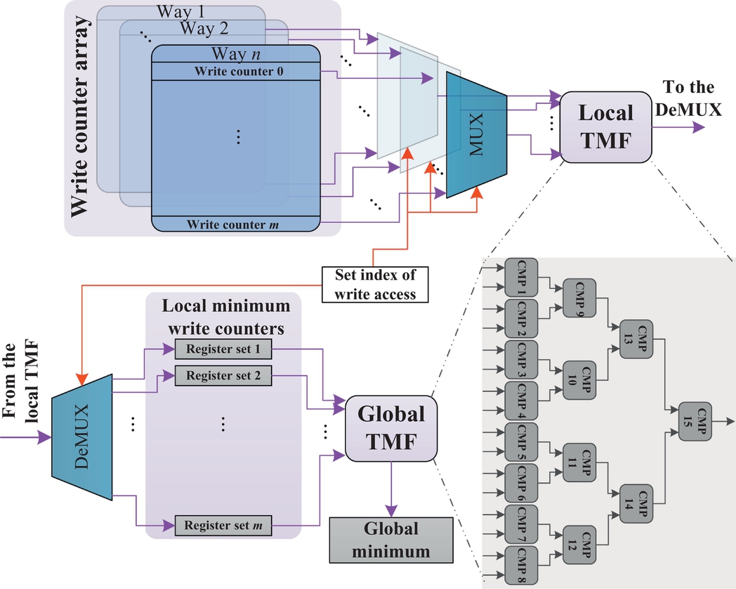
Each of the parameters mentioned in Table 3 is a function of WT, which is dependent on the behavior of the applications themselves. The feedback from changes in these parameters during the runtime of an application can be used to regulate WT. However, such an approach is sensitive to the details of the implementation. In other words, the question, is how much should the variation in the aforementioned parameters change the WT? Additionally, the appropriate relation between these parameters and WT may differ in various applications. These complexities motivate us to employ a mechanism that has the least possible dependency to the behavior of running applications. To this end, we propose a new structure, DTR, in order to effectively take these parameters into account for regulating WT, without having to deal with the complexities mentioned before. Fig. 14 depicts DTR. It simply sets WT to the minimum value of WCs in LR.
Using the minimum value of WCs in LR mimics the desired behavior mentioned in Table 3. First, WHitLR is roughly related to the minimum value of WCs in LR. In other words, growth in WHitLR results in increase in the min(WCs) most of the time, hence the WT goes up. Second, min(WCs) creates meritorious data blocks into LR. This results in two desired consequences: first, unnecessary Swaps are avoided; second, min(WCs) will probably increase per swap.
WHitHR is another factor that must affect WT. However, WHitHR cannot be considered directly by our proposal. To overcome this issue, we look at the number of writes per block in TWWS of different applications. By setting the maximum possible value of the WC to the average of writes per block in TWWS, the WCs will probably be reset at the end of the lifetime of the blocks in TWWS. This naturally prevents the WCs from keeping large values and hence averts directing the majority of write operations to HR.
We use two tree-structured minimum-finder (TMF) units, each comprising 15 comparators to find min(WCs). One of the TMFs, the local TMF, is responsible for determining the minimum WC value per set. On each write access, the WCs’ value of the corresponding set are directed to the local TMF by MUXes, and the minimum WCs of that set are updated via a DEMUX. The other TMF, the global TMF, updates the global minimum of the WCs in LR, using the local minima of sets.
The proposed mechanism can easily adapt itself to the behavior of applications, without having to deal with the complexities of determining the proper coefficients for WHitLR, WHitHR, and Swap values in making decisions about the value of WT. The only dependency of our design to the behavior of the application is the maximum possible value of WCs that we set to the average of writes per block in the TWWS of applications (see Table 2) in our experiments.
6 Implementation
In this section, we elaborate on the details of the implementation of our proposed architecture. The structure of LR, LR and HR retention times, bit-width of counters, and detailed parameters of cache latencies and power, in addition to the overhead of our design are discussed.
LR cache size and structure
Regarding the average size of TWWS in Table 2, we opt to set the size of LR to 256 blocks. Ideally, we want LR to keep the TWWS of the workload and HR to keep the read-only blocks. It is obvious that structures with higher associativities provide higher LR utilizations, but due to their higher complexity, they are not appropriate for large caches. On the other hand, direct-mapped structure has the least complexity, but the least utilization, too. Because the size of LR in our design is small, we adopt a high associativity. Fig. 15 shows different latency and energy values of LR with different associativities. By enhancing associativity, latency and dynamic power increase insignificantly, but LR utilization increases dramatically. Thus we set the associativity of LR to 16, because it yields proper utilization and reasonable energy/latency. In addition, with such an associativity level, our two comparator trees in DTR incur the least overhead of area and latency (i.e., two 15-comparator trees for our 16 × 16 LR structure).
LR and HR cache retention times
With respect to Fig. 12A and B, LR and HR retention times are selected to be 100 μs [52] and 40 ms [43], respectively. For each cache line, there are 4-bit counters working at 160 kHz in LR to track data retention, and 2-bit counters are used in HR working at 100 Hz. The use of larger RCs in LR is due to the lower retention time of blocks in this part of the cache, which requires a more accurate refreshing mechanism. Therefore a higher bit width enables tracking smaller slots of time, which leads to more accuracy [43].
As stated previously, the maximum possible value of WCs (i.e., 64) is selected based on the average write accesses per block in TWWS in Table 2.
The main overhead of the proposed architecture includes RCs, WCs, LR-to-HR and HR-to-LR buffers, and DAACS and DTR logics. The total capacity of RCs, WCs, and buffers is 6 KB, which is less than 1% of the cache capacity. Table 4 demonstrates the details of latencies and energies of LR, HR, and buffers extracted from CACTI 6.5 and its modified version [58, 59]. DAACS and DTR logics, on the other hand, incur an area overhead of less than 3% in our design.
Table 4
Detailed Structural Parameters of L2 Cache
| Data Array | Tag Array | |||||||||
| Technology | Cache Size (KB) | RL (ns) | WL (ns) | RE (nJ) | WE (nJ) | RL (ns) | WL (ns) | RE (pJ) | WE (pJ) | Leakage Power (mW) |
| SRAM | 384 | 0.596 | 0.538 | 0.048 | 0.021 | 0.242 | 0.157 | 1.03 | 0.520 | 48.79 |
| STT-RAM (HR-LR) | 1472–64 | 0.556–0.489 | 3.17–1.10 | 0.024–0.029 | 0.166–0.072 | 0.296–0.225 | 0.211–0.140 | 1.88–1.64 | 1.32–0.653 | 2.632 |
| Buffer LR-to-HR | 2 | 0.323 | 0.280 | 0.0105 | 0.0017 | – | – | – | – | 3.875 |
| Buffer HR-to-LR | 2 | 0.323 | 0.280 | 0.0105 | 0.0017 | – | – | – | – | 4.059 |
Notes: RE, read energy; RL, read latency; WE, write energy; WL, write latency.
7 Evaluation Result
To evaluate the proposed architecture, a GPGPU-Sim3.2.1 simulator [26] was used to simulate PTX commands at cycle level. The simulator mimics the behavior of SMs, L2 cache, interconnection network, and off-chip main memory, and three groups of benchmarks were considered: (1) benchmarks provided with the simulator [26], (2) Rodinia [60], and (3) Parboil [61]. We used the CUDA version of the benchmarks in our experiments.
According to the investigations carried out in Ref. [62], GPGPU applications are divided into two general categories based on their behavior: cache-insensitive and cache-sensitive, where the first is called a cache-unfriendly application and the latter is called a cache-friendly application. Note that increasing the cache size can increase the performance of some applications, while some other applications do not benefit from larger cache sizes. Of course, the area saved as a result of replacing the SRAM L2 by the STT-RAM L2 can be used to add new components that cause an application to run faster. We chose register files as a case study for two reasons: first, register files are one of the bottlenecks in assigning TBs to SMs in GPUs [63]; second, devoting the area saved by replacing the cache to the register files is a fair assumption, as register files in GPUs are large, highly banked SRAM arrays with a structure similar to that of cache [40]. Therefore enhancing the GPU with extra register files is beneficiary. The applications with larger register files are indicated by “*” in Table 2.
In order to have a fair comparison, we used the saved area for additional resources in two ways: the saved area is used to accommodate a larger L2 cache, or the saved area is used for enlarging the register files. Because the STT-RAM cell is 4× denser than the SRAM cell, the simulations were done for two configurations: extra cache (EC), replacing L2 with an STT-RAM cache of the same area (i.e., a 4× larger L2 cache); and an extra register file (ER), replacing L2 with a same-sized STT-RAM cache where the saved area is used for implementing 15% larger register files in SMs.
Note that because in our configuration, area of data array is at least 80× that of tag array, we keep the tag array SRAM because it is fast and its area overhead remains insignificant. Table 5 shows these configurations based on the GTX480 structure. Simulation results are compared to the baseline GPU with SRAM L2 and EC and ER scenarios. We simulated baseline uniform caches with STT-RAM cells of 10-year and 40-ms retention times to show the effectiveness of our mechanism.
Table 5
GPGPU-Sim Configurations
| Baseline GPU | 15 cluster, 1 SM/cluster, L1 D cache: 4-way 16 KB 128B line, Const. cache: 8 KB 128B line, |
| Text. cache: 12 KB 64B line, Instr. cache: 2 KB 128 line, Shared memory: 48 KB, No. memory | |
| controller: 6, Interconnect topology: Butterfly, Technology node: 40 nm, 32,768 register | |
| 32-bit width, 384 KB 8-way 256B line L2 cache | |
| Baseline | 32,768 register, 1536 KB 8-way L2 cache |
| STT-RAM | |
| EC | 32,768 register, 1472 KB 8-way HR 64 KB 16-way LR L2 cache |
| ER | 37,684 register, 320 KB 8-way HR 64 KB 16-way LR L2 cache |
Fig. 16A and B shows the execution time and IPC values with respect to the SRAM baseline system. The applications are sorted in ascending order by the achieved IPC improvement in our proposal. As can be seen in Fig. 16A, the execution time of fixed and dynamic threshold mechanisms are, respectively, reduced by 16% and 17%.
About half of the applications (from backprop to histo in Fig. 16B) are not cache-sensitive; hence they do not benefit from the proposed architecture in terms of IPC. The other half (from bfs-p to kmeans in Fig. 16B), on the other hand, enjoy up to 2.7× IPC gains. Overall, the proposed L2 architecture results in an average of 20.7% improvement in terms of IPC. It must be noted that these improvements are only 3% and 13.4% for baselines with STT-RAM cells of 10-year and 40-ms retention times, respectively. However, we could increase the IPC improvement to 18.8% and 20.7% by applying fixed and dynamic threshold techniques. A remarkable point is that applications like MUM, lavaMD, and Gaussian are cache-sensitive and suffer from high latency of the baseline STT-RAM L2 cache, and our proposal effectively overcomes this issue by employing the LR part for storing frequently written data blocks. For some of the applications marked with “*” in Table 2, no speedup is gained because the enhanced register file could not help the GPU assign more thread blocks to an SM.
Note that in most cases, IPC and execution time results have correlations, although in some cases, such as streamcluster, there is more improvement in the execution time.
Fig. 16C shows the dynamic energy consumed by different architectures (normalized to that of the SRAM baseline system). Dynamic energy consumption in STT-RAM architectures is high due to the write energy of MTJ cells. The write energy in STT-RAM cells is more than SRAM cells even after reducing their retention time. Because of large values of the dynamic energy for baseline STT-RAM with cells of 10-year retention time, we omitted its results from the figures. On average, it consumed 6.7× more dynamic energy in comparison to the SRAM baseline. Designs with fixed and dynamic thresholds impose an overhead of 74.9% and 52.6% to dynamic energy, respectively. As can be seen, the dynamic threshold technique reduces the overhead by 22.3%. The STT-RAM baseline with retention time of 40 ms has a dynamic energy of 2.5× of the SRAM baseline. Note that for lbm, srad-v1, heartwall, nw, and RAY, the dynamic energy consumption of the baseline STT-RAM with cells of 40 ms retention time is less than that of the design with a fixed threshold. However, our proposed dynamic threshold scheme overcomes this problem. This is mainly due to the efficient migration of blocks between the LR and HR parts in the proposed architecture.
As the leakage power of magnetic memory cells is negligible, the average total power consumption of the whole L2 cache has reduced by 20.3% and 28.9% when using fixed and dynamic threshold schemes, respectively, compared to the SRAM baseline system. It is noteworthy that the STT-RAM baseline system with cells of 40 ms retention time has consumed 9.9% more energy with respect to the SRAM baseline system, despite its lower leakage power.
As discussed previously, to have most of the rewrites as block refreshers, a relatively high-retention time is needed to be set. For example, for a retention time of 5 ms, around 89% of rewrites are used as block refreshers. However, a significant portion of rewrites can be used as refreshes in lower retention times (with 100 μs retention time, this fraction is around 36%). This behavior was observed in most of the applications. Thus it is efficient to have a split design in order to exploit this opportunity, and at the same time, to avoid paying the excessive cost of refresh overhead in a nonsplit low-retention cache. In order to demonstrate that the split cache design is an optimal choice rather than uniform but low-retention time cache, we also conducted simulations with 100 μs, 300 μs, 500 μs, 5 ms, and 40 ms retention times. In these designs, around 36%, 46%, 50%, 89%, and 100% of the rewrites act as refreshes, respectively. Fig. 17 shows that performance degrades by an increase in the retention time. However, this degradation is not linear. This is because, with a low-retention time, a large number of refreshes are required, which block the accesses to cache. This issue is better observed by analyzing the power consumption. Increasing the retention time to more than 500 μs results in significant write energy. In addition to that, for retention times lower than 500 μs, the refreshing overhead increases the power consumption. Our split cache design, however, outperforms all nonsplit cache designs in terms of performance and power consumption.
7.1 Lifetime Evaluation
Although endurance of the STT-RAM cache is not a concern in this work, we have investigated the effects of our proposed architecture on the lifetime of the cache. To do so, we used the equation presented in Ref. [53]. Fig. 18 demonstrates intra and interset variations for both HR and LR in the proposed architecture with respect to the baseline nonsplit STT-RAM cache. Using our dynamic threshold mechanism, intra and interset variations had improvements of 4.79% and 21.8%, respectively. This is due to the fact that we moved frequently written blocks to LR, and consequently the migration of data blocks from LR to HR results in a more even distribution of writes on cache blocks in HR, which is critical for lifetime. Intra and interset variation improvements for LR are 79% and 68%, respectively. The reason for these large improvements is that a significant portion of the writes are conducted in LR, with a relatively small size. This large number of writes in a small cache results in a more uniform write distribution. Because there are different retention times, write variation and count are not the only factors affecting the lifetime. It was shown that lifetime and write energy are directly related to each other [64–66]. This fact can be used to calculate the lifetime of the LR and HR part. Table 6 demonstrates the lifetime improvement (LI) values for LR and HR. The third column shows the LI for the whole cache structure, which is the minimum of the LI values of LR and HR parts. Our results show that the lifetime is improved by up to 336% (111%, on average) with respect to the baseline.
Table 6
LI of HR and LR Parts
| Workloads | HR Part LI (%) | LR Part LI (%) | Cache LI (%) | Workloads | HR Part LI (%) | LR Part LI (%) | Cache LI (%) |
| backprop | 186 | 426 | 186 | bfs-p | 212 | 548 | 212 |
| bfs | 233 | 280 | 233 | cfd | 77 | −4 | −4 |
| cutcp | 30 | 32 | 30 | gaussian | 329 | 190 | 190 |
| heartwall | 83 | 409 | 83 | histo | 20 | −30 | −30 |
| hotspot | 76 | 1400 | 76 | kmeans | 17 | −37 | −37 |
| lavaMD | 53 | 239 | 53 | lbm | 158 | 37 | 37 |
| leukocyte | 51 | 198 | 51 | LIB | 91 | 1735 | 91 |
| LPS | 101 | 6861 | 101 | lud | 199 | 1993 | 199 |
| mri-gridding | 108 | 222 | 108 | mri-q | 102 | 7558 | 102 |
| MUM | 232 | 2194 | 232 | myocyte | 1039 | 336 | 336 |
| nw | 171 | 4531 | 171 | pathfinder | 56 | 13,142 | 56 |
| RAY | 127 | 560 | 127 | sad | 160 | 9652 | 160 |
| sgemm | −27 | 90,768 | −27 | spmv | 159 | 21,242 | 159 |
| srad-v1 | 125 | 18,432 | 125 | srad-v2 | 150 | 53,818 | 150 |
| stencil | 118 | 14 | 14 | STO | 184 | 510 | 184 |
| tpacf | 82 | 3260 | 9 | Avg. | 152 | 7760 | 111 |
7.2 Parallel vs Sequential Search Mechanism
Fig. 19 shows the dynamic power consumption reduction and performance overhead of the DAACS, in comparison to the parallel search mechanism. The figure shows an average reduction of 38.9% in the power consumption of the cache controller. Note that the performance overhead of using the power-efficient DAACS with respect to the parallel search mechanism is negligible (about 1%). This is mainly due to the efficient LR and HR block mapping and migration mechanisms we adopted.
8 Conclusion
Current trends in VLSI technology and GPU architectures show that future GPUs should have larger L2 caches with a proportionally larger power consumption. Due to the desirable properties of STT-RAM devices (low leakage power and high density), STT-RAM can replace SRAM L2 caches in the future GPU architectures. However, the high write latency and energy of STT-RAM are two main drawbacks that have to be dealt with before it can replace SRAM. STT-RAM cells with lower retention times can be employed to remedy the latency and energy problems of write operations, but they require refreshing. This chapter proposed a two-part STT-RAM L2 cache architecture for GPUs based on a detailed workload investigation of GPGPU applications. We proposed to keep frequently written blocks in a small low-retention part of the cache, while less frequently written, high frequently read blocks are mapped to the high-retention part of the cache. The decision regarding the mapping of data blocks to the low-retention or high-retention part was made based on a dynamic threshold for the number of write operations carried out on the data blocks in the high-retention part. Our evaluations showed that our architecture could effectively improve IPC by up to 170% (20.7%, on average), while average L2 cache energy consumption is improved by 28.9%, as compared to the conventional SRAM-based L2 architecture in current GPUs.