Common-emitter power amplifiers: a different perception?
Now and again articles appear in Electronics World that provoke thought. The sum-of-squares principle of Mr Williams sounded most intriguing, so I ran a few simulations to see if the linearity it could provide was an improvement over conventionality. This proved not to be the case, but it did lead to an interesting intellectual journey. As usually happens when I am evaluating an idea, enough work had been done for an chapter on the topic, and here it is.
When I read Michael William’s intriguing article Making a Linear Difference to Square-Law fets,1 I was attracted by the prospect of applying it to an audio power output stage. I found the phrase ‘curvilinear class A’ particularly appealing.
The basic concept of the difference-of-squares is not new, as several correspondents to EW + WW have pointed out.2,3 Another early reference (1949) to the quarter-squares principle can be found in the monumental MIT Radiation Lab series on radar techniques.
Mr William’s basic circuit is shown in Figure 1, and the first problem to overcome in applying it for audio power is that the wanted output is the difference of two currents whereas hard-bitten amplifier designers are more used to a low impedance voltage output. Note that with the usual enhancement-mode power fets, if V1, V2 are a.c. sources only, and carry no d.c. bias, then Vb will have to establish point M some volts below ground. No doubt something could be done with industrial-sized current-mirrors, but it struck me that the circuit could be rearranged as Figure 2, by making use of complementary devices. We now need two bias voltages Vb1, Vb2, and the positioning of the two signal sources V1, V2 on opposite rails looks a little awkward, but at least the current-difference will be mathematically perfect, if Kirchhoff has anything to say on the matter.

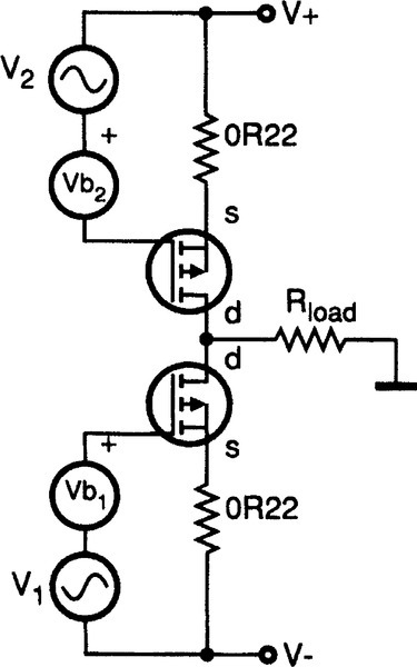
So far so good. We now have a single current output iout. But is this any use for driving loudspeakers? I am assuming that current-drive of speakers is not the final goal; I appreciate that this can be made to work, and promises some tempting advantages in terms of reducing bass-unit distortion.4 My immediate reaction to Figure 2 was no, it can’t work, because with a high impedance output, the output stage gain will vary wildly with load impedance making the amount of NFB applied a highly variable quantity. It would also appear that any capacitive loading of this high-impedance node would generate an immediate output pole that would make stable compensation a waking nightmare.
However, just as I was discarding the notion, it occurred to me that the structure in Figure 2 looks very much like the bipolar common emitter (CE) stage in Figure 3. This is widely used in low voltage opamps because the low saturation voltage allows a close approach to the rails.5 The more usual emitter follower type of opamp output is usually called a CC or common-collector stage. It is highly probable that the widest application of these voltage-efficient CE configurations is in the headphone amplifiers of personal stereos.

At about the same time I encountered a paper by Cherry6 which pointed out that, so long as NFB is applied, the output impedance of such a stage can be as low as for the usual voltage follower type output. Cherry’s paper is dauntingly mathematical, so I will summarise it thus. The vital point about using NFB to reduce the output impedance of an amplifier is that the amount of NFB applied must be calculated assuming that the open-loop case is unloaded. This condition looks unfamiliar, because the average amplifier usually has a fairly low output resistance even when open-loop, due to its output follower configuration, and so the loaded/unloaded distinction makes only a negligible difference when calculating the reduction of output resistance by NFB.
Using this condition, Cherry shows that output impedance of a CE stage should be exactly equivalent to the usual CC stage, when the global NFB is applied. I appreciate that this result is counter-intuitive; it looks as though the current output version must have a higher output impedance, even with NFB, but it appears not to be so. Doubters who are unafraid of matrix algebra should consult Cherry’s paper.
Topology to the test
Nonetheless, before reaching for the power fets, I felt the need for further reassurance that a CE output stage was workable. There are several low voltage opamps that use the CE output topology, so it seemed instructive to provoke one of these with some output capacitance and see what happens. A suitable candidate is the Analog Devices AD820, which has a BJT output stage looking like Figure 3 and provides all you need for CE experimentation in one 8-pin package.7
My practical findings were that the opamp works well, and while THD may not be up to the very best standards, it was happy with varying load resistances, proved stable with capacitors hung directly on the output, and was relaxed about rail decoupling. Once again, so far, so good.
By this stage, the quarter-squares principle was slipping somewhat into the background. My attention was focusing on the possibilities of a BJT power output stage something like Figure 4, which shows the addition of drivers and emitter resistors to make the circuit more practical. A good output swing is facilitated by the inward-facing driver arrangement. In a conventional emitter follower output the need to leave the drivers room to work in further reduces output swing.

Figure 4 could be configured into something like a normal Class-B amp, except that the novel use of a CE output stage would allow greater efficiency than usual because there would be the low Vce(sat) drops mentioned above. Also the crossover behaviour would presumably be different from a normal CC output, and quite possibly better, or at least more easily manipulated.
In a previous article8 I tried to demonstrate that for an amplifier in which all the easily manipulated distortion mechanisms had been suitably dealt with, the low frequency THD was below the noise when driving an 8 Ω load. This without large global feedback factors: 30 dB at 20 kHz is quite adequate.
At high frequencies (say above 2 kHz) the distortion is easily measurable, and almost all of its results from crossover effects in the output stage. Since NFB typically falls with frequency, these high-order harmonics receive much less linearisation. This is why any technique that promises a reduction in basic crossover nonlinearity is of immediate interest to those concerned with power amplifier design.
I began to think that Mr Williams had opened up a whole new field of audio amplification; each conventional CC output stage would have its dual in CE topology, perhaps with new and exciting characteristics.
The next stage of the investigation was more sobering. There was a familiarity about CE output stages. Readers old enough to recall paying 30 shillings for their first OC72 will recognise Figure 5 as the configuration used almost universally for low power audio output for many years when there was no such thing as a complementary device. Transformers provide one way to make a push-pull output. At first sight bias voltage Vb looks as if it will be far too low but bear in mind these are germanium transistors. Note the upside-down format of the circuit which is typical of the period. The circuit values are appropriate for an output of about 500 mW.
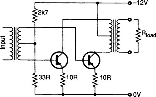
While it is perhaps not obvious, this is the equivalent of Figure 3. The need for an npn is avoided by using phase inversions in the transformers. So clearly CE output stages were not as rare and specialised as I thought; however they might still have handy distortion properties that were not obvious in the long-gone days of transformer coupling.
Adding Spice to the investigation
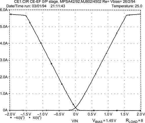
The next step was Spice simulation of the practical BJT output circuit in Figure 4: Figure 6 shows how the device currents vary in a relationship that looks ominously like classic Class-B. Somehow I was expecting more overlap of conduction. The linearity results are presented in Figure 7 as a plot of incremental gain versus output voltage for varying loads, as in the Distortion In Power Amplifiers series.8

The first obvious difference is that stage gain, instead of staying close to unity, varies hugely with load impedance – pretty much what we expect from a CE stage operating open-loop. Note that the X-axis is V1 (V2 =−V1 to induce push-pull operation) and so represents the input voltage only rather than both input and output as before. Multiplying this input voltage by the gain taken from the Y-axis gives the peak output voltage swing. The vertical gain drop-offs that indicate clipping move inwards with higher load impedances because of the greater output gain rather than through any hidden limitation on output swing.
Figure 8 shows the effect of varying the bias, and hence quiescent current, for an 8-Ω load.
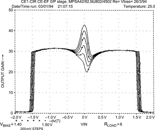
This circuit certainly works, but some how the linearity results seem depressingly familiar. There is the same gain-wobble at crossover we have seen ad nauseam with CC output stages, and once again there is no bias setting that removes or significantly smooths it out. As before, the usual falling-with-frequency NFB will not deal with this sort of high-order distortion very effectively, leading to a rise in THD above the noise in the upper audio band.
In fact, the characteristics look so suspiciously similar to the standard emitter-follower CC stage, that it began to belatedly dawn on me they might actually be the same thing …
Figure 9 shows the final stages of this conceptual hejira. Figure 9(a) shows the simplified circuit of Figure 3 with the power supplies V +, V-included; they no doubt come from a mains transformer so we can float them at will, and it seems quite in order to pluck them from their present position and put them in the collectors of the output devices instead. All the other supplies shown are equally without ties forming an independent unit with the associated transistor and emitter resistor Re. Thus they cannot affect device currents. Since there is only one ground reference in the circuit, it is also a legitimate gambit to put it wherever we like, which in this case is now the opposite end of the load R1. (See Ref. 9 for another example of this manoeuvre). This gives us the unlikely looking but functionally equivalent circuit in Figure 9(b).
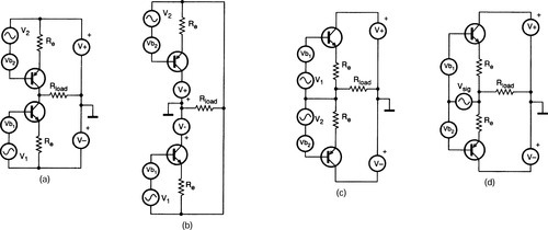
A purely cosmetic rearrangement of Figure 9(b) produces Figure 9(c), which is topologically identical, and reveals that the new output stage is … a CC stage after all. Figure 9(d) shows the standard output.
The only true difference between the ‘CE’ stage and the traditional CC stage is the arrangement of the two bias voltages Vb1, Vb2. In a conventional CC stage, the output bases or gates are held apart by a single fixed voltage, shown here as Vb1 and Vb2 connected together. This rigid ‘unit’ can be regarded as driven with respect to the output rail by the signal source Vsig, representing the difference between input and output of the stage. Normally, of course, it is more useful to regard the earlier circuitry as generating a signal voltage with respect to ground.
In contrast to Figure 9(d), Figure 9(c) has two bias voltage generators, and the consequence of this is that voltage drops in the emitter resistors Re are not coupled across to the opposite device by the bias voltage. This does not seem to offer immediately any magical stratagems for reducing the gain deviation around crossover, and creates the need for two drive voltages referenced about the output rail. This should be fairly easy to contrive, but is bound to be more complex than the traditional method.
Squaring the circle
Having gone through these manipulations, it is time to reconsider fets and the quarter-squares approach, knowing now that we are dealing with something very close to a standard power-amp configuration. To underline the point. Figure 10 shows the gain characteristics for the circuit of Figure 2, using 2SK135/2SJ50 power fets. Note the very close resemblance to a conventional source follower.8

As Mr Williams points out, the Vgs/Id characteristic curve for power fets may follow a square law at low currents, but it is more or less linear at high ones, and this appears to rule out any simple approach to ‘curvilinear class A’. For the fets I used, the ‘square lawish’ region is actually tiny, being roughly between 0 to 80 mA which is of limited use for a power stage. In so far as second-harmonic cancellation occurs at all, it is in the crossover region where, without this effect, the central gain deviations would probably be greater than they are.
As I can see, the quarter-squares concept is already in use in most FET power amplifiers in heavy disguise but only operational in the crossover region. If this idea is to be pursued further, we need a true square-law output device. Since there is no such thing, it would need to be realised by some kind of law-synthesis circuitry. If amplifier distortion needs reducing below the tiny levels possible with relatively conventional techniques, there are probably better avenues to explore.