Cool audio power
I have always thought that some kinds of information cry out to be presented graphically. A case in point is the ultimate destination of the power that an amplifier draws from its supply. Some goes usefully into the load, some is dissipated in the power semiconductors, and a little is lost in drivers, emitter resistors, and so on. All these quantities vary strongly with the percentage power output, and they overlap to give a confused and uninformative picture if plotted on a normal graph. The alternative method of power-partition diagrams, presented here, shows at once how much is power is taken and precisely where it goes; this is particularly important for more complex output stages, such as Class-G types. The idea is not wholly original; my inspiration came from what Victorian engineers called Sankey diagrams, a similar method of showing where the energy went in a large steam engine.
This chapter only deals with sinusoidal waveforms, for reasons explained at the start of the chapter. I feel bound to point that I was perfectly aware that sine waves and musical waveforms have little in common, but you have to start somewhere, and a waveform that allows you to easily check your simulator results against pure mathematics has some pretty strong advantages.
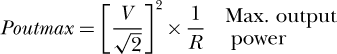
There are several important power relationships in designing an output stage. Both the average and peak power dissipated in the output devices must be considered when determining their type and number. The average power dissipated controls the heat-sink design.
In most amplifier types the power dissipation varies strongly with output signal amplitude as it goes from zero to maximum, so the information is best presented as a graph of dissipation against the fraction of the available rail-to-rail output swing – i.e., the output voltage fraction.
Consideration of average power allows the output devices to be made thermally safe; but it is also essential to consider the peak instantaneous dissipation in them. Audio waveforms have large low-frequency components, too slow for peak currents and powers to be allowed to exceed the DC limits on the data sheet.
For a resistive load the peak power is fixed and easily calculable. With a reactive load the peak power excursions are less easy to determine but highly important because they are increased by the changed voltage/phase relationships in the output device. Thus for a given load impedance modulus the peak power would need to be plotted against load phase angle as well as output fraction to give a complete picture.
Average power drawn from the rails is also a vital prerequisite for the power-supply design; since the rail voltage is substantially constant this can be easily converted into a current demand, which must be known when sizing reservoir capacitors, choosing rectifiers, and so on.
The voltage rating of these components is a much simpler business, requiring simply that they withstand the off-load voltages at the maximum mains voltage, which is usually taken as 10% above nominal. The only thing to decide is how big a safety margin is required.
Power drawn depends on signal-level and is again conveniently displayed with voltage-fraction as the X-axis.
The mathematical approach
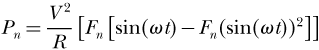
When dealing with power amplifier efficiency, most textbooks use a purely mathematical method as shown in Figure 1, which was produced with the aid of Mathcad. The calculation gives only the dissipation in the power devices.

Figure 1 gives the familiar information that maximum device dissipation occurs at 64% of maximum voltage, equivalent to 42% of maximum power. These specific numbers are a result of the sine waveform chosen and other waveforms give different values.
To make it mathematically tractable, the situation is highly idealised, assuming an exact 50% conduction period, no losses in emitter resistors or Vce(sat) s, and so on. Solving the problem for Class AB, where the conduction period varies with signal amplitude, is considerably more complex due to the varying integration limits.
Simulating dissipation
Alternatively, the power variations in real output stages can be simulated and the results plotted; the circuits simulated in this article are shown in Figure 2.

For concision, and by analogy with logic outputs, I have called the upper transistor the source and the lower the sink. In simulation, losses and circuit imperfections are included, and the power dissipations in every part of the circuit, including power drawn from the supply rails, are made available by a single run.
It is an obvious choice – which I duly took – to use a sine waveform in the simulations. This allows a reality-check against the mathematical results. Reactive loads are easily handled, so long as it is appreciated that the simulation often has to be run for ten or more cycles to allow the conditions in the load to reach a steady state.

Instantaneous power dissipation
Integrate over one half cycle
![]()
![]()
Note the 1/π due to integration from 0 to π
![]()
Since only one device conducts at once, dissipation for one is total dissipation
![]()
All simulations were run with ± 50 V rails and an 8 Ω resistive or reactive load. The output emitter resistors were 0.1 Ω. The drawback to this approach is that it is rather labour intensive. With my current simulation software, PSpice 6.0 for DOS, the steps are:
• Simulate the output stage over a whole cycle, for each input voltage fraction; 5% steps give enough points for a presentable curve; the ●STEP command automates this.
• Display simulation results in the graphical post-processor. (In PSpice this is called PROBE) This assumes it can display computed quantities, e.g., Vce × Ic to give instantaneous device-power. Peak and average results can be read from the same display as PROBE. There is a function called AVG, which – unsurprisingly – yields the running average over a cycle. This stage can be automated as a macro, which is just as well, since it has to be performed at least 20 times, once for each input fraction value.
• The awkward bit. The computed peak and averaged power dissipations at the end of the cycle are read out from the PROBE cursor and recorded by hand, for each value of input fraction. There seems to be no other way to extract the information.
• The data from the third step is typed into Mathcad, to produce the graphs shown in this article. Once the data has been entered, Mathcad can manipulate it in almost any way conceivable.
Power-partition diagrams
The graph in Figure 1 gives only one quantity, the amplifier dissipation.
I suggest a more informative graph format that I call a power partition diagram, which shows how the input power divides between amplifier dissipation, useful power in the load, and losses in drivers, etc.
Power dissipations are plotted against the input voltage fraction; this is not quite the same as the output voltage fraction as these are real output stages with gain slightly less than one. The input fraction increases in steps of 0.05, stopping at 0.95 to avoid clipping. The X-axis may linear or logarithmic.
Figure 3 shows the power-partition diagram for a Class-B complementary feedback pair stage as in Figure 2, which has a low quiescent current. Line 1 plots the Pdiss in the sink (lower) device. Line 2 is source plus sink power. Line 3 is source plus sink plus load power.
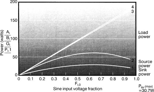
The topmost line 4 is the total power drawn from the power supply, and so the narrow region between 3 and 4 is the power dissipated in the rest of the circuit – mainly the drivers and the output emitter resistors Re. This power increases with output drive, but remains negligible compared with the other quantities examined.
The diagram shows immediately that the power drawn from the supply increases proportionally to the drive voltage fraction. This is partitioned between the load – represented by the curved region between lines 2 and 3 – and the output devices. Note how the peak in their power dissipation accommodates the curve of the load power as it increases with the square of the voltage fraction.
Figure 4 shows the same diagram for a Class-B emitter-follower output stage. The quiescent current of an emitter follower output stage is significant – here 150 mA – and pushes up the power dissipation around zero output, but at higher levels the curves are the same. There is no need for extra heatsinking over the complementary feedback pair case.

Effects of increased bias
Figure 5 shows Class-AB, with bias increased so that Class-A operation and linearity is maintained up to 5 W r.m.s. output.

The quiescent current has increased to 370 mA, so quiescent power dissipation is significantly higher for output fractions below 0.1. Device dissipation is still greatest at a drive fraction of around 0.6, so once again no extra cooling is required to deal with the increased quiescent dissipation.
A push-pull Class-A amplifier draws a large standing current, and the picture looks totally different; see Figure 6. The power drawn from the supply is constant, but as output increases dissipation transfers from the output devices to the load, so minimum amplifier heating is at maximum output.

The significant point is that amplifier dissipation is only meaningfully reduced at a voltage fraction of 0.5 or more, i.e. only 6 dB from clipping. Compared with Class-B, an enormous amount of energy is wasted internally.
Single-ended or constant-current versions of Class-A have even lower efficiency, worse linearity, and no corresponding advantages.
Class G
Hitachi introduced the Class-G concept in 1976 with the aim of reducing amplifier power dissipation by exploiting the high peak-mean ratio of music.1 I have recently explained its operation in Ref. 2.
At low outputs, power is drawn from a pair of low-voltage rails; for the relatively infrequent excursions into high power, higher rails are drawn from. Here the lower rails are ± 15 V, 30% of the higher ± 50 V rails, so I call this Class G (30%).
This gives a discontinuous power-partition diagram, as in Figure 7. Line 1 is the dissipation in the low-voltage inner source device, which is kept low by the small voltages across it. Line 2 adds the dissipation in the high-voltage outer source; this is zero below the rail-switching threshold.

Above this are added the identical – due to symmetry – dissipations in the inner and outer sink devices, as Lines 3 and 4. Line 5 adds the power in the load, and Line 6 is the total power drawn, as before.
Power consumption and amplifier dissipation at low outputs are much reduced; above the threshold these quantities are only slightly less than for Class-B. Class-G does not show its power-saving abilities well under sinewave drive.
Class-B and reactive loads
The simulation method outlined above is also suitable for reactive loads. It is however necessary to run the simulation not just for one cycle, but sometimes for as many as twenty. This is to ensure that steady-state conditions have been reached.
The diagrams referred to below are for steady-state 200 Hz sinewave drive; the frequency must be defined so the load impedance can be set by suitable component values, but otherwise makes no difference.
Figure 8 shows what happens in Class-B emitter follower when driving a 45° capacitive-reactive load with a modulus of 8 Ω. Comparing it with Figure 4, the power drawn from the supply is essentially unchanged, and is still proportional to output voltage fraction.

The larger areas at the bottom show that more power is being dissipated in the output devices and correspondingly less in the load, because the phase shift causes the voltage across and the current through the output devices to overlap more. The amplifier must dispose of 95 W of heat worstcase, rather than 60 W.
Average device dissipation no longer peaks, but increases monotonically up to maximum output. 45° phase angles are common when loudspeakers are driven. It is generally accepted that an amplifier should be able to provide full voltage swing into such a load.
When the load is purely reactive, with a phase angle of 90°, it can dissipate no power and so all that delivered to it is re-absorbed and dissipated in the amplifier. Figure 9 shows that the worst-case device dissipation is much greater at 185 W, absorbing all the power drawn from the supply, and therefore necessarily increasing monotonically with output level; there is no maximum at medium levels.

This is a very severe test for a power amplifier. It is also unrealistic, as no assemblage of moving-coil speaker elements can ever present a purely reactive impedance; 60° loads are normally the most reactive catered for. Table 1 shows the worst-case cycle-averaged dissipation for various load angles, showing how the position of maximum dissipation moves towards full output as the angle increases.
Table 1
| Angle (°) | Pdiss(max) (W) | Voltage fraction |
| 0 | 60 | 0.64 |
| 10 | 63 | 0.65 |
| 20 | 67 | 0.70 |
| 30 | 70 | 0.75 |
| 45 | 95 | 0.95 |
| 60 | 115 | 1.00 |
| 90 | 185 | 1.00 |
This is best displayed in 3D, as Figure 10, which plots power vertically; the slight hump at the front – non-reactive load – disappearing as the load becomes more reactive.
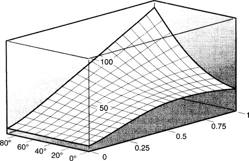
The dissipation hump is of little practical significance. An audio amplifier will almost certainly be required to drive 45° loads, and these cause higher power dissipations than resistive loads driven at any level.
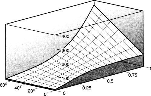
Figure 11 shows the same plot for peak power, which increases monotonically with both output fraction and load angle. Figure 12 summarises all this data for design purposes. It shows worst-case peak and average power in one output device against load reactance.
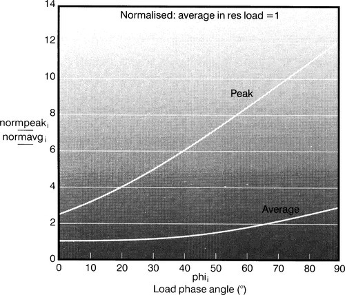
Peak powers are taken at 0.95 of full output, average power at whatever output fraction gives maximum dissipation. Therefore to design an amplifier to cope with 45° loads, note that average power is increased by 1.4 times, and peak power by 2.7 times, over the resistive case. This can mean that it is necessary to increase the number of output devices simply to cope with the much enhanced peak power.
Considering simple reactive loads like those listed in the panel ‘Reactive load observations’ gives an essential insight into the extra stresses they impose on semiconductors but is still some way removed from real signals and real loudspeaker loads, where the impedance modulus varies along with the phase, due to electromechanical resonances or crossover dips.
I looked at single and two-unit loudspeaker models in Ref. 3 where the maximum phase angle found was 40°. In brief, the results were:
• Amplifier power consumption and average supply current drawn vary with frequency due to impedance modulus changes.
• The peak device current increased by a maximum of 1.3 times at the modulus minima.
• The average current in the output devices increased by a maximum of 1.3 times.
• Peak device power increased by a maximum factor of 2, mostly due to phase shift rather than impedance dips.
• Average device dissipation increased by a maximum of 1.4 times.
These numbers come from two specific models that attempted to represent ‘average’ speakers. Worse conditions could easily have been found.
Ultimately a comprehensive survey of the loudspeakers on the market would be required, but this would be very time-consuming. In Ref. 4, which gives an excellent account of real speaker loading, 21 models were tested and the worst angle found was 67°. Eliminating the two most extreme cases reduced this to 60°.
The most severe effect of reactive loads is the increase in peak power, followed by the increase in average power.
Both are a strong function of load phase, and so the specification of the maximum angle to be driven has a big effect on the devices required, heat-sink design, and hence on amplifier cost.
It is likely that a failure to appreciate just how quickly peak power increases with load angle is the root cause of many amplifier failures.