
Distortion in power amplifiers, Part III: the voltage-amplifier stage
The voltage-amplifier stage (or VAS) has often been regarded as the most critical part of a power-amplifier, since it not only provides all the voltage gain but also must deliver the full output voltage swing. This is in contrast to the input stage which may give substantial transconductance gain, but the output is in the form of a current. But as is common in audio design, all is not quite as it appears. A well-designed voltage amplifier stage will contribute relatively little to the overall distortion total of an amplifier, and if even the simplest steps are taken to linearise it further, its contribution sinks out of sight.
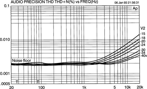
As a starting point, Figure 1 shows the distortion plot of a model amplifier with a Class-A output (± 15 V rails, + 16 dBu out). The model is as described in previous articles. No special precautions have been taken to linearise the input stage or the VAS and output stage distortion is negligible. It can be seen that the distortion is below the noise floor at low frequencies; the distortion slowly rising from about 1 kHz is coming from the voltage amplifier stage. At higher frequencies, where the VAS 6 dB/octave rise becomes combined with the 12 or 18 dB/octave rise of input stage distortion, we can see the accelerating distortion slope typical of many amplifier designs.

The main reason why the voltage amplifier stage generates relatively little distortion is because at LF, global feedback linearises the whole amplifier, while at HF the voltage amplifier stage is linearised by local negative feedback through Cdom.
Examining the mechanism
Isolating the voltage amplifier stage distortion for study requires the input pair to be specially linearised, or else its steeply rising distortion characteristic will swamp the VAS contribution. This is most easily done by degenerating the input stage which also reduces the open-loop gain. The reduced feedback factor mercilessly exposes voltage amplifier stage nonlinearity. This is shown in Figure 2, where the 6 dB/octave slope suggests origination in the VAS, and increases with frequency solely because the compensation is rolling-off the global feedback factor.
Confirming that this distortion is due solely to the voltage amplifier stage requires varying VAS linearity experimentally while leaving other circuit parameters unchanged. Figure 3 achieves this by varying the VAS negative rail voltage; this varies the proportion of its characteristic over which the voltage amplifier stage swings, and thus only alters the effective VAS linearity, as the important input stage conditions remain unchanged. The current-mirror must go up and down with the VAS emitter for correct operation, and so the Vce of the input devices also varies, but this has no significant effect as can be proved by the unchanged behaviour on inserting cascode stages in the input transistor collectors.

The typical topology as shown in Figure 4(a) is a classical common emitter voltage amplifier stage with a current-drive input into the base. The small-signal characteristics, which set open-loop gain and so on, can be usefully simulated by the spice model shown in Figure 5, of a VAS reduced to its conceptual essentials. G is a current source whose value is controlled by the voltage-difference between Rin and Rf2, and represents the differential transconductance input stage. F represents the voltage amplifier stage transistor, and is a current source yielding a current of beta times that sensed flowing through ammeter V which, by spice convention, is a voltage source set to 0 V.


The value of beta, representing current-gain, models the relationship between VAS collector current and base current. Rc represents the total stage collector impedance, a typical real value being 22 kΩ. With suitable parameter values, this simple model provides a useful demonstration of relationships between gain, dominant-pole frequency, and input stage current outlined in the first article in this series. Injecting a small signal current into the output node from an extra current source also allows the fall of impedance with frequency to be examined.
The overall voltage gain clearly depends linearly on beta, which in real transistors may vary widely. Working on the trusty engineering principle that what cannot be controlled must be made irrelevant, local shunt NFB through Cdom sets the crucial HF gain that controls Nyquist stability. The LF gain below the dominant pole frequency P1 remains variable (and therefore so does P1) but is ultimately of little importance; if there is an adequate NFB factor for overall linearisation at HF then there are unlikely to be problems at LF where gain is highest. As for the input stage, the linearity of the voltage amplifier stage is not greatly affected by transistor type, given a reasonably high beta value.
Stage distortion
Voltage amplifier stage distortion arises from a curved transfer characteristic of the common-emitter amplifier, a small portion of an exponential.1 This characteristic generates predominantly second-harmonic distortion, which, in a closed-loop amplifier, will increase at 6 dB/octave with frequency.
Distortion does not get worse for more powerful amplifiers as the stage traverses a constant proportion of its characteristic as the supply-rails are increased. This is not true of the input stage: increasing output swing increases the demands on the transconductance amp as the current to drive Cdom increases. The increased Vce of the input devices does not measurably affect their linearity.
It seems ironic that VAS distortion only becomes clearly visible when the input pair is excessively degenerated – a pious intention to ‘linearise before applying feedback’ can make the closed loop distortion worse by reducing the open loop gain and hence the NFB factor available to linearise the VAS. In a real (non-model) amplifier with a distortive output stage, the deterioration will be worse.
The local open-loop gain of the VAS (that existing inside the local feedback loop closed by Cdom) should be high, so that the voltage amplifier stage can be linearised. This precludes a simple resistive load. Increasing the value of Rc will decrease the collector current of the transistor reducing its transconductance. This reduces voltage gain to the starting value.
One way to ensure sufficient gain is to use an active load. Either bootstrapping or a current source will do this effectively, though the current source is perhaps more dependable and is the usual choice for hi-fi or professional amplifiers.
The bootstrap promises more output swing as the collector of Tr4 can soar above the positive rail. This suits applications such as automotive power amps that must make the best possible use of a restricted supply voltage.2
These two active-load techniques also ensure enough current to drive the upper half of the output stage in a positive direction right up to the supply rail. If the collector load were a simple resistor, this capability would certainly be lacking.
Checking the effectiveness of these measures is straightforward. The collector impedance may be determined by shunting the collector node to ground with decreasing resistance until the open loop gain falls by 6 dB indicating that the collector impedance is equal to the current value of the test resistor.
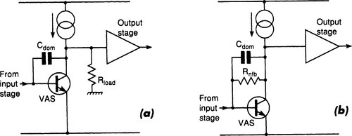
The popular current source version is shown in Figure 4(a). This works well, though the collector impedance is limited by the effective output resistance Ro of the voltage amplifier stage and the current source transistors3 which is another way of saying that the improvement is limited by Early effect.
It is often stated that this topology provides current-drive to the output stage; this is only partly true. It is important to realise that once the local NFB loop has been closed by adding Cdom the impedance at the VAS output falls at 6 dB/octave for frequencies above P1. The impedance is only a few kΩ at 10 kHz, and this hardly qualifies as current-drive at all.
Bootstrapping (Figure 4(b)) works in most respects as well as a current source load, for all its old-fashioned flavour. The method has been criticised for prolonging recovery from clipping. I have no evidence to offer on this myself, but I can state that a subtle drawback definitely exists: LF open loop gain is dependent on amplifier output loading. The effectiveness of bootstrapping depends crucially on the output stage gain being unity or very close to it. However the presence of the output transistor emitter resistors means that there will be a load-dependant gain loss in the output stage significantly altering the amount by which the VAS collector impedance is increased. Hence the LF feedback factor is dynamically altered by the impedance characteristics of the loudspeaker load and the spectral distribution of the source material.
This has significance if the load is a quality speaker with impedance modulus down to 2 Ω, in which case the gain loss is serious. If anyone needs a new audio-impairment mechanism to fret about, then I offer this one in the confident belief that its effects, while measurable, are not of audible significance.
The standing d.c. current also varies with rail voltage. Since accurate setting and maintaining of quiescent current is difficult enough, an extra source of possible variation is decidedly unwelcome.
A less well known but more dependable form of bootstrapping is available if the amplifier incorporates a unity gain buffer between the VAS collector and the output stage as shown in Figure 4(f), where Rc is the collector load, defining the VAS collector current by establishing the Vbe of the buffer transistor across itself. This is constant, and Rc is therefore bootstrapped and appears to the VAS collector as a constant current source.
In this sort of topology a voltage amplifier stage current of 3 mA is quite sufficient, compared with the 6 mA standing current in the buffer stage. The voltage amplifier stage would in fact work well with collector currents down to 1 mA, but this tends to compromise linearity at the high-frequency, high-voltage corner of the operating envelope, as the VAS collector current is the only source for driving current into Cdom.
Voltage stage enhancements
Figure 2, which shows only VAS distortion, clearly indicates the need for further improvement over that given inherently by the presence of Cdom if an amplifier is to avoid distortion. While the virtuous approach might be an attempt to straighten the curved voltage amplifier stage characteristic, in practice the simplest method is to increase the amount of local negative feedback through this capacitance. Equation 1 in the first article shows that the LF gain (i.e. the gain before Cdom is connected) is the product of input stage transconductance, Tr4 beta and the collector impedance Rc. The last two factors represent the VAS gain and therefore the amount of local NFB can be augmented by increasing either. Note that so long as the value of Cdom remains the same, the global feedback factor at HF is unchanged and so stability is not affected.
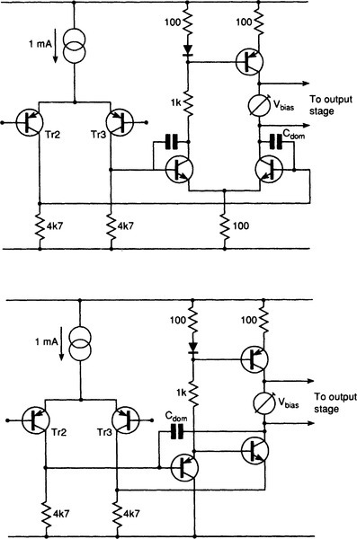
The effective beta of the stage can be substantially increased by replacing the VAS transistor with a Darlington, Figure 4(c). Adding an extra stage to a feedback amplifier always requires thought because, if significant additional phase-shift is introduced, the global loop stability may suffer. In this case the new stage is inside the Miller loop and so there is little likelihood of trouble. The function of such an emitter follower is sometimes described as ‘buffering the input stage from the VAS’ but its true function is linearisation by enhancement of local NFB.
Alternatively the stage collector impedance may be increased for higher local gain. This is could be done with a cascode configuration (Figure 4(d)) but the technique is only useful when driving a linear impedance rather than a Class-B output stage with its non-linear input impedance.
Assuming for the moment that this problem is dealt with, either by use of a Class-A output or by VAS-buffering, the drop in distortion is dramatic as is the beta-enhancement method. The gain increase is ultimately limited by Early effect in the cascode and current source transistors, and more seriously by the loading effect of the next stage. But it is of the order of 10 times and gives a useful improvement.
This is shown by curves A, B in Figure 6 where the input stage of a model amplifier has been over-degenerated with 100 Ω emitter resistors to bring out the voltage amplifier stage distortion more clearly.
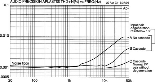
Note that in both cases the slope of the distortion increase is 6 dB/octave. Curve C shows the result when a standard undegenerated input pair is combined with the cascoded VAS; the distortion is submerged in the noise floor for most of the audio band, being well below 0.001%.
This justifies my assertion that input stage and VAS distortion need not be a problem; we have all but eliminated distortions 1 and 2 from the list of seven given in the first article.
A cascode transistor also allows the use of a high-beta transistor for the voltage amplifier stage; these typically have a limited Vceo that cannot withstand the high rail voltages of a high-power amplifier. There is a small loss of available voltage swing, but only about 300 mV, which is usually tolerable. Experiment shows that there is nothing to be gained by cascoding the current source collector load.
A cascode topology is often used to improve frequency response by isolating the upper collector from the Cbc of the lower transistor. In this case the frequency response is deliberately defined by a well defined passive component.
It is hard to say which technique is preferable; the emitter follower circuit is slightly simpler than the cascode version, which requires extra bias components, but the cost difference is minimal. When wrestling with these kind of financial decisions it as well to remember that the cost of a small-signal transistor is often less than a fiftieth of that of an output device, and the entire small-signal section of an amplifier usually represents less than 1% of the total cost, when heavy metal such as the mains transformer and heatsinks are included.
Benefits of voltage drive
The fundamentals of linear voltage amplifier stage operation require that the collector impedance is high, and not subject to external perturbations. Thus a Class-B output stage, with large input impedance variations around the crossover point, is the worst possible load. The ‘standard’ amplifier configuration deserves tribute that it can handle this internal unpleasantness gracefully, 100 W/8 Ω distortion typically degrading only from 0.0008% to 0.0017% at 1 kHz assuming that the avoidable distortions have been eliminated. Note however that the effect becomes greater as the global feedback factor is reduced. There is little deterioration at HF, where other distortions dominate.4
The VAS buffer is most useful when LF distortion is already low, as it removes Distortion 4, which is – or should be – only visible when grosser non-linearities have been seen to. Two equally effective ways of buffering are shown in Figures 4(e) and 4(f).
There are other potential benefits to VAS buffering. The effect of beta mismatches in the output stage halves is minimised.5 Voltage drive also promises the highest fT from the output devices, and therefore potentially greater stability, though I have no data of my own to offer on this point. It is right and proper to feel trepidation about inserting another stage in an amplifier with global feedback, but since this is an emitter follower its phase shift is minimal and it works well in practice.
A VAS buffer put the right way up can implement a form of d.c. coupled bootstrapping that is electrically very similar to providing the voltage amplifier stage with a separate current-source.
The use of a buffer is essential if a VAS cascode is to do some good. Figure 7 shows before/after distortion for a full-scale power amplifier with cascode VAS driving 100 W into 8 Ω.

Balanced voltage amplifier stage
When linearising an amplifier before adding negative feedback one of the few specific recommendations made is usually the use of a balanced voltage amplifier stage – sometimes combined with a double input stage consisting of two differential amplifiers, one complementary to the other. The latter seems to have little to recommend it, as you cannot balance a stage that is already balanced, but a balanced (and, by implication, more linear) voltage amplifier stage has its attractions. However, as explained above, the distortion contribution from a properly designed VAS is negligible under most circumstances, and therefore there seems to be little to be gained.
Two possible versions are shown in Figure 8; The first type gives approximately 10 dB more open loop gain than the standard, but this naturally requires an increase in Cdom if the same stability margins are to be maintained. In a model amplifier, any improvement in linearity can be wholly explained by this o/l gain increase, so this seems (not unexpectedly) an unpromising approach. Also, as John Linsley Hood has pointed out,6 the standing current through the bias generator is ill-defined compared with the usual current source VAS. Similarly the balance of the input pair is likely to be poor compared with the current-mirror version. Two signal paths from the input stage to the VAS output must have the same bandwidth; if they do not then a pole-zero doublet is generated in the open-loop gain characteristic that will markedly increase settling-time after a transient. This seems likely to apply to all balanced voltage amplifier stage configurations. The second type is attributed by Borbely to Lender,7 Figure 8 shows one version, with a quasi-balanced drive to the VAS transistor, via both base and emitter. This configuration does not give good balance of the input pair since it depends on the tolerances of R2, R3, the Vbe of the voltage amplifier stage, and so on. Borbely has advocated using two complementary versions of this giving a third type, but this would not seem to overcome the objections and the increase in complexity is significant.
All balanced voltage amplifier stages seem to be open to the objection that the vital balance of the input pair is not guaranteed, and that the current through the bias generator is not well-defined. However one advantage would seem to be the potential for sourcing and sinking large currents into Cdom, which might improve the ultimate slew-rate and HF linearity of a very fast amplifier.
Open loop bandwidth
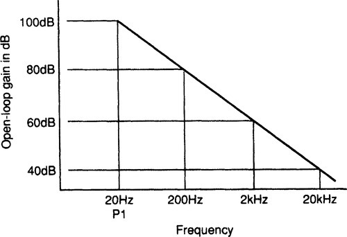
Acute marketing men will appreciate that reducing the LF open loop gain, leaving HF gain unchanged, must move the P1 frequency upwards, as shown in Figure 9. Open loop gain held constant up to 2 kHz appears so much better than open loop bandwidth restricted to 20 Hz. These two statements could describe near identical amplifiers, except that the first has plenty of open loop gain at LF while the second has even more. Both amplifiers have the same feedback factor at HF, where the amount available has a direct effect on distortion performance, and could easily have the same slew rate. Nonetheless the second amplifier somehow reads as sluggish and indolent, even when the truth of the matter is known.
Reducing low frequency open loop gain may be of interest to commercial practitioners but it also has its place in the dogma of the subjectivist. Consider it this way: firstly there is no engineering justification for it and, secondly, reducing the NFB factor will reveal more of the output stage distortion. NFB is the only weapon available to deal with this second item so blunting its edge seems ill-advised.
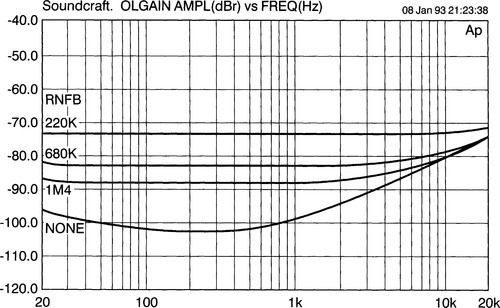
It is of course simple to reduce open loop gain by degenerating the input pair, but this diminishes it at HF as well as LF. To alter it at LF only requires engineering changes at the VAS. Figure 10 shows two ways. Figure 10(a) reduces gain by reducing the value of the collector impedance, having previously raised it with the use of a current source collector load. This is no way to treat a gain stage: loading resistors low enough to have a significant effect cause unwanted current variations in the VAS as well as shunting its high collector impedance, and serious LF distortion appears. While this sort of practice has been advocated in E&WW in the past,8 it seems to have nothing to recommend it. Figure 10(b) also reduces overall open loop gain by adding a frequency insensitive component to the local shunt feedback around the voltage amplifier stage. The value of RNFB is too high to load the collector significantly and therefore the full gain is available for local feedback at LF, even before Cdom comes into action. Figure 11 shows the effect on the open loop gain of a model amplifier for several values of RNFB; this plot is in the format described in the first part of this series where error voltage is plotted rather than gain so the curve appears upside down compared with the usual presentation. Note that the dominant pole frequency is increased from 800 Hz to above 20 kHz by using a 220 kΩ value for RNFB; however the gain at higher frequencies is unaffected and so is the stability. Although the amount of feedback available at 1 kHz has been decreased by nearly 20 dB, the distortion at + 16 dBu output is only increased from below 0.001% to 0.0013%. Most of the reading is due to noise.
In contrast, reducing the open loop gain by just 10 dB through loading the VAS collector to ground requires a load of 4.7kΩ which, under the same conditions, yields distortion of more than 0.01%.
It might seem that the stage which provides all the voltage gain and swing in an amplifier is a prime suspect for generating the major part of its non-linearity. In actual fact, this is unlikely to be true, particularly with a cascode VAS/current source collector load buffered from the output stage. Number 2 in the distortion list can usually be forgotten.