Sound mosfet design
This was the first article on power amplifiers that I wrote, though I had been designing them for manufacture since 1975. This investigation into the concept of combining power FET output devices with bipolar drivers was done some years before I undertook my major investigation into the root causes of power amplifier distortion. (See Distortion in Power Amplifiers, Parts 1–8, later in this book.) In the throes of the design process, I realised with greater force than hitherto that the distortions in the small-signal part of a power amplifier were (a) far from negligible and (b) susceptible to analysis by a mixture of SPICE simulation and a few well-chosen experiments. I also determined that SPICE could be extremely useful in the analysis of output stages. The rest is history.
I have resisted the temptation to edit the text in the light of later knowledge, as this would, I think, be cheating. To prevent people being misled, I will just point out that the final circuit falls somewhat short of the Blameless performance standards set by the Distortion in Power Amplifiers series. The input stage may look symmetrical, but in fact is grotesquely unbalanced, with 16 μA flowing through the left transistor of the pair, and 580 μA through the right. This stage must have generated far more second-harmonic distortion than necessary, and with the benefit of hindsight I am not very proud of it. This imbalance also means that the input stage transconductance is far too low, which precludes any emitter degeneration of the input pair, and this also explains why a dominant-pole capacitor as small as 15 pF is enough for stability. The voltage-amplifier stage could be improved in linearity by adding another transistor within the Cdom local feedback loop.
Mosfet amplifiers undoubtedly present a tantalising prospect for simple circuitry. Unfortunately, practical application requires careful consideration of their many foibles. But my aim here is to stimulate thinking about possible improvements to FET power amps, and describe two new avenues of development. Each produces a practical result, though neither should be regarded as a foolproof recipe for success.
Power-amplifier design is as prone as any other branch of audio to folklore and confusion. One of the less extreme myths holds that high levels of negative feedback are ‘A Bad Thing’ because they require heavier compensation for HF stability, leading to low slew rates and generally indolent and sluggish behaviour.
As far as it goes this is true. But only a poor designer would lose all sight of slew rate while adjusting amplifier compensation. Despite much study of TIM, DIM, SID, ‘internal overload’, ‘delayed feedback’ and the rest, everything comes back to slew rate.
If an amplifier can reproduce a 20 kHz sine wave at full amplitude without excessive distortion (say under 0.1%) it can be regarded as blameless in respect of speed. Apply as much feedback as is decent, but always keep an eye on stability and slew rate.
Design fundamentals
Ground rules for this design study require DC output coupling, one preset only (for quiescent current) and as simple a circuit as possible.
In the current audio market, almost any technological approach appears to be acceptable (an idiosyncratic hybrid with valves driving power fets is one recent design,1) with the possible exception of capacitor output coupling.
While problems can include capacitor distortion at LF (of the real and measurable kind2) and perhaps grounding difficulties, the overwhelming simplicity of this method still has its attractions; the almost unnatural reliability of the capacitor-coupled Quad 303 should be mentioned at this point.
But a designer must still prove that he knows what a differential pair is, and d.c. coupling has therefore been adopted. However, remember that proper offset protection is not a trivial problem, as the cost of a reliable output relay and d.c. detection circuitry can add 30% to amplifier electronics costs. A relay seems unavoidable, as my own experiences with kamikaze crowbars have been distinctly unhappy, though I would not claim this to be a definitive judgment.
So a simple unregulated power supply looks to be the best. I realise this brings me into head-to-head confrontation with Mr Linsley Hood,3 so I shall quickly explain my preference.
Putting expensive power semiconductors in a high-current dual supply can easily double an amplifier’s electronic-component cost and there is much more to go wrong.
Ensuring PSU HF stability can be difficult, and the PSU compensation required, threatening a steadily rising output impedance versus frequency, can lead to some awkward amplifier stability problems.
Finally, the unregulated supply can deliver more power on a transient basis – which is exactly what is required for audio.
The price to be paid for unregulated simplicity is the attention to be paid to the amplifier’s supply-rail rejection. But since it is physically impossible for the voltage on large reservoir capacitors to change very quickly, this rejection need only be extremely good at low frequencies.
The excellent supply-rail rejection of IC op-amps – and a power amplifier is, after all, only a big op-amp – shows the problem to be distinctly soluble, although I admit that op-amp PSRR often differs markedly between the two rails, and usually declines above 1 kHz. This sort of difficulty can be simply solved in a power amplifier with a little RC decoupling.
Harmonic distortion should be kept as low as possible, but without spending significant money specifically on its reduction. THD in commercial equipment varies more widely than any other performance parameter, ranging from 0.003% to 1% at similar powers4 with the most expensive units often giving the worst performance.
In marketing circles, there are clearly two routes to take: make the THD vanishingly small to show you know what you’re doing; or make it poor and imply that this very practical parameter has been sacrificed in favour of some intangible and unmeasurable sonic benefit.
I have always gone for the former and so have concentrated on linearity as being the prime determinant of amplifier topology.
Distortion performance is not easy to specify completely, ideally requiring a spectrum analysis of every combination of level, frequency and load impedance. But this is not practical and so I have summarised it as THD plotted against frequency, into 8 Ω, at different levels where appropriate.
Pros and cons of mosfet output devices have been thoroughly ventilated, 5,6 but one point needs qualification. They have been praised for having a large crossover region between the two halves of a Class B stage, but my experiments show this to be a very dubious advantage.
Mosfet outputs, with or without the augmentations described below, may be uncritical of quiescent current setting, but this really means that nothing is exactly right. Bipolar stages, with sharper crossover regions, do at least make it obvious where to set the quiescent current, providing it is set by observing the distortion residual – and it certainly should be.
Mosfet distortion residuals typically present a rather gnarled appearance, with plenty of harmonics at least to the seventh. Though it runs counter to conventional wisdom, in my experience complementary-pair bipolar residuals tend to be smoother.
Another vital point is that mosfet complementary-pairs are rare, not particularly complementary, and definitely more expensive than the profusion of strictly N-channel devices intended for switching.
Determining performance
Mosfet power amps have suffered more than most branches of technology from ‘application-note cloning’ though some original designs have been published, ranging from the complex7,8 to the very complex.9 These are well worth ferreting out, though perhaps unattractive commercially.
The ‘standard’ mosfet amplifier circuit (Figure 1) differs from the equally standard bipolar-style circuit (Figure 2) mainly in possessing a sort of push–pull/current-mirror configuration in the voltage amplifier stage, probably intended to provide better charge/discharge of the mosfet input capacitances. This stage is sometimes called the pre-driver, but it is less confusing to call the first full-voltage-swing stage ‘the voltage amplifier stage’, or VAS.

The first question to be asked is what improvement is made by this push–pull arrangement (Figure 3). The linearity is not very different and the benefit at HF is not startling. As always in science, it pays to be skeptical.

Given that the simpler bipolar configuration of Figure 2 is workable, there are established ways to improve its overall linearity and some of these are shown in Figure 4.

Linearity can be enhanced simply by increasing open-loop gain (Figure 4a and b) or by a cascode arrangement (Figure 4c) which attempts to linearise the VAS by eliminating Early effect. Cascode arrangements are relatively ineffective at reducing distortion in power amplifiers, since the Early effect seems to be dominated by non-linear loading of the high impedance at the interface with the output stage (points A and B).
The added emitter-follower and current-mirror enhancements (Figure 4a and b) work because the input pair act as a transconductance amplifier (voltage-difference in, current out) feeding a VAS that is basically a Miller integrator, thanks to the dominant-pole capacitance C dom.
Emitter-follower Tr3 increases open-loop gain by enhancing the currentgain of the VAS. The current mirror does the same thing by doubling inputpair transconductance; also slew-rate is greater and symmetrical (30 V/μs was obtained) as the input stage can now sink current as effectively as it sources it. Furthermore, input collector currents are kept balanced, valuable if the d.c. offset at the amplifier output is to be kept within acceptable bounds (say ± 50 mV) without adjustment. The input collector currents, and hence the base currents drawn through input and feedback resistors, must be roughly equal.
Total input pair current is a critical parameter, since it affects input-stage transconductance and hence open-loop gain, and also defines the maximum slew rate, setting the maximum current that can flow in and out of the dominant-pole compensation capacitor Cdom. Though not obvious, the input-pair current is an important influence on the HF stability of the amplifier. Power amplifier design has always been impeded by the fact that the crucial VAS, with its high-impedance collector, has to drive an output stage with markedly non-linear input impedance. The resulting interaction means that, when distortion occurs, it is not clear whether it arises in the output stage itself, or at the VAS due to non-linear loading.
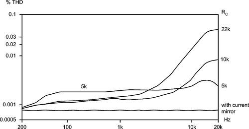
Distortion not caused by the output can be studied by replacing the output stage with a very linear Class-A voltage-follower. Resistor Rc has a strong effect on HF distortion (Figure 5) with a clear improvement when Rc is replaced by a simple diode/transistor current mirror. This underlines the crucial nature of the interface between the input pair and the VAS.
Similarly, the output stage can be tested in isolation by driving it directly from a low-impedance oscillator6 and this technique was used to study the two output arrangements described below.
Neither method, however, allows study of the VAS/output interaction directly. One strategy for side-stepping this problem is to use a unity-gain buffer between the VAS and the nonlinear load of the output stage (e.g. emitter-follower Tr4 , Figure 4d).
This approach has not been pursued with mosfets, but I have used it in a commercial design for a bipolar quasi-complementary amplifier. It proved effective at reducing distortion and is an approach which seems unfairly neglected.
Reducing costs
In the search for a better amplifier, two routes were examined. The first is to reduce the cost of a mosfet power amp by using two N-channel devices in a form of quasi-complementary output stage.
The second is to increase linearity and improve quiescent stability by using bipolar drivers with local feedback around each output FET.
The quasi-complementary approach is directly analogous to that used in the early days of transistor amplifiers; a P-N-P transistor is combined with an N-channel FET to emulate a P-channel FET, and this works very well.
The output devices are now the same (promising bulk-buying economy) and can be chosen without reference to complements. That used was the IRF530, offering 100 V, 14 A, and 75 W in a TO-220 package, a pair costing £5.00 against £9.50 for the 2SK134/2SJ49 pair. Open-loop distortion of the output stage alone driven from a low impedance was shown (Figure 6) to be 1.1%.

Closed-loop performance (Figure 7), (yielded by the practical circuit shown in Figure 8) demonstrated that, predictably, output symmetry is not wonderful, and crossover effects on the residual were clear.


But this performance is acceptable from such a simple and economical circuit, and could almost certainly be improved at minor cost by adopting added emitter-follower and/or current mirror.
Tests showed that the value of Rc in Figure 8 is non-critical, so there seems no difficulty in driving the bottom mosfet gate capacitance.
Quiescent setting is by transistor bias-generator; this is purely a regulator, and is not thermally coupled to the output devices. In an attempt to improve output symmetry, a Baxandall diode10 was inserted at point D in the driver emitter. Sadly, THD was unchanged, despite the dependable improvement that this modification gives in bipolar quasi-complementary designs.
Reducing distortion
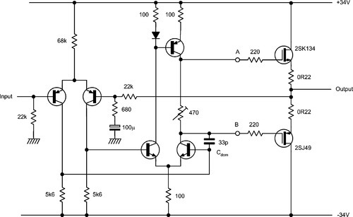
If performance outweighs economy, a true complementary output pair is retained, with local feedback linearising each mosfet.6 An important variable here is the value of emitter-resistor Re in Figure 11. A high value increases output distortion, since it reduces the feedback factor within each hybrid bipolar-mosfet loop, while a low value makes quiescent-current setting unduly critical. As a compromise, 10–22 Ω works well.
Figure 9 shows the output stage alone in open loop giving 0.05%, and Figure 10 shows closed-loop performance as given by the practical design in Figure 11, plus the effect of varying Cdom.


An emitter-follower is added to increase the feedback factor, and Cf is now needed for HF stability with Cdom = 15 pF. The compensation is not necessarily optimised for all possible real-life loads.
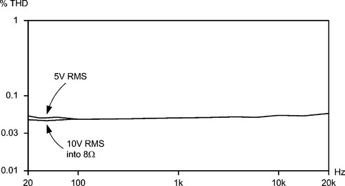
Distortion across the band is now very low. While it is desirable to define the closed-loop bandwidth of any audio device, do not put a simple RC filter at the input, as this makes the bandwidth dependent on the output impedance of the upstream equipment.
The temptation to implement it by increasing Cf should also be resisted, because if it is large enough to provide a suitable roll-off, there is a danger that it will induce mysterious VHF instability in Tr2 – a common effect. It is only revealed by distortion that vanishes at the touch of a cautious finger.
I have not tried to give the final word on this subject, though I hope it illuminates a few new directions. The use of current mirror topology in particular looks promising.