Distortion in power amplifiers, Part VII: frequency compensation and real designs
The distortion performance of an amplifier is determined not only by open loop linearity, but also the negative feedback factor applied when the loop is closed. In most practical circumstances doubling the NFB factor halves the distortion. To date, this series has focused on basic circuit linearity. I have assumed that open loop gain falls at 6 dB/octave due to a single dominant pole, with the amount of NFB permissible at HF being set by the demands of HF stability. Because of this, the distortion residuals from a ‘blameless’ amplifier are comprised almost entirely of crossover artifacts due to their high frequency content. Audio amplifiers using more advanced compensation are rather rare. However, certain techniques do exist …
This series has stuck close to conventional topologies, because even commonplace circuitry has been shown to have little known aspects and interesting possibilities. This implies a two-gain-stage circuit (unity gain output stages not being counted) with most of the feedback applied globally, but smoothly transferred to the voltage amplifier stage alone as frequency increases. Other configurations are possible; a one stage amplifier is an intriguing possibility – they are common in cmos op-amps – but is probably ill-suited to power amp impedances. See Ref. 1 for an eccentric three-stage amplifier with an open loop gain of just 52 dB (due to the dogged use of local feedback) and only 20 dB of global feedback. Most of the section below refers only to the conventional two-stage structure.
Making a pole dominant
Dominant pole compensation is the simplest kind, though its implementation involves subtlety. Simply take the lowest pole to hand (PI), and make it dominant, i.e. so much lower in frequency than the next pole P2 that the total loop gain (the open loop gain as reduced by the attenuation in the feedback network) falls below unity before enough phase shift accumulates to cause HF oscillation. With a single pole, the gain must fall at 6 dB/octave, corresponding to a constant 90° phase shift. Thus the phase margin will be 90° giving good stability. Figure 1(a) shows the traditional Miller method of making a dominant pole. The collector pole of Tr4 is lowered by adding the Miller capacitance Cdom to that which unavoidably exists as the Cbc of the VAS transistor. However there are other beneficial effects; Cdom causes ‘pole splitting’, in which the pole at Tr2 collector is pushed up in frequency as P1 moves down – most desirable for stability. Simultaneously the local NFB through Cdom linearises the VAS.

Assuming that input stage transconductance is set to a plausible 5 mA/V, and stability considerations set the maximal 20 kHz open loop gain to 50 dB, then from the equations in Part 1, Cdom must be 125 pF. This is more than enough to swamp the internal capacitances of the VAS transistor, and is a realistic value.
The peak current that flows in and out of this capacitor for an output of 20 V r.m.s., 20 kHz, is 447 μA. Recalling that the input stage must sink Cdom current while the VAS collector load sources it, and likewise the input stage must source it while the VAS sinks it, there are four possible places in which slew rate might be limited by inadequate current capacity. If the input stage is properly designed then the usual limiting factor is VAS current sourcing. In this example a peak current of less than 0.5 mA should be easy to deal with, and the maximum frequency for unslewed output will be comfortably above 20 kHz.
Figure 1(b) shows a much less satisfactory method – the addition of capacitance to ground from the VAS collector. This is usually called shunt lag compensation, and as Peter Baxandall aptly put it, ‘The technique is in all respects sub-optimal’.2
We have already seen in Part 3 that loading the VAS collector resistively to ground is a very poor option for reducing LF open loop gain, and a similar argument shows that capacitive loading to ground for compensation purposes is an even worse idea. To reduce open loop gain at 20 kHz to 50 dB as before, the shunt capacitor Clag must be 43.6 nF, which is a whole different order of things from 125 pF. The current flowing in Clag at 20 V r.m.s., 20 kHz, is 155 mA peak, which is going to require some serious electronics to provide it. This important result can be derived by simple calculation, and I have confirmed it with Spice simulation. The input stage no longer constrains the slew rate limits, which now depend entirely on the VAS.
A VAS working under these conditions is almost certain to have poor linearity. The current variations in the stage, caused by the extra loading, produces more distortion and there is now no local NFB through a Miller capacitor to correct it. To make matters worse, the dominant pole P1 will probably need to be set to a lower frequency than for the Miller case, to maintain the same stability margins, as there is now no pole splitting to raise the pole at the input stage collector. Hence Clag may have to be even larger, and require even higher peak currents. Takahashi has produced a fascinating paper on this approach,3 showing one way of heaving about the enormous compensation currents required for good slew rates. The only thing missing is an explanation of why shunt compensation was chosen in the first place.
Including the output stage
Miller capacitor compensation elegantly solves several problems at once, and the decision to use it is not hard. However the question of whether to include the output stage in the Miller feedback loop is less easy. Such inclusion (see Figure 1(c)) presents the desirable possibility that local feedback could linearise both the VAS and the output stage, with just the input stage left out in the cold as frequency rises and global NFB falls. This idea is most attractive as it would greatly increase the feedback available to linearise a Class B output stage.
There is certainly some truth in this where applying Cdom around the output as well as the Vas reduced the peak 1 kHz THD from 0.05% to 0.02%.4 However, it should be pointed out that the output stage was deliberately under biased to induce crossover spikes because, with optimal bias, the improvement was too small to be either convincing or worthwhile. Also, this demonstration used a model amplifier with TO-92 ‘output’ transistors. In my experience this technique just does not work with real power bipolars because it induces intractable HF oscillation.
The use of local NFB to linearise the VAS demands a tight loop with minimal extra phase shift beyond that inherent in the Cdom dominant pole. It is permissible to insert a cascode or a small signal emitter follower into this local loop, but a sluggish output stage seems to be pushing the phase margin too far; the output stage poles are now included in the loop, which loses its dependable HF stability. Bob Widlar has stated that output stage behaviour must be well controlled up to 100 MHz for the technique to be reliable.5 This would appear to be virtually impossible for discrete power stages with varying loads.
While I have so far not found ‘Inclusive Miller compensation’ to be workable myself, others may know different. If anyone can shed further light I would be most interested.
Nested feedback loops
Nested feedback is a way to apply more NFB around the output stage without increasing the global feedback factor. The output has an extra voltage gain stage bolted on, and a local feedback loop is closed around these two stages. This NFB around the composite block reduces output stage distortion and increases frequency response, to make it safe to include in the global NFB loop.
Suppose that block A1 (Figure 2(a)) is a distortionless small signal amplifier providing all the open loop gain and so including the dominant pole. A3 is a unity gain output stage with its own main pole at 1 MHz and distortion of 1% under given conditions: this 1 MHz pole puts a firm limit on the amount of global NFB that can be safely applied.
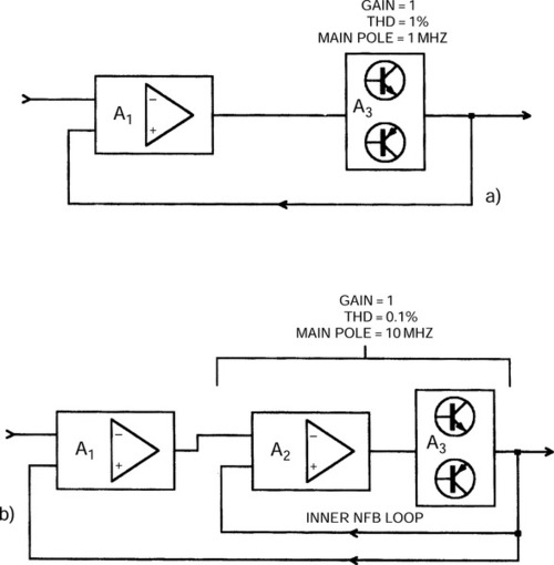
Figure 2(b) shows a nested feedback version; an extra gain block A2 has been added, with local feedback around the output stage. A3 has the modest gain of 20 dB so there is a good chance of stability when this loop is closed to bring the gain of A3 + A2 back to unity. A2 now experiences 20 dB of NFB, bringing the distortion down to 0.1%, and raising the main pole to 10 MHz, which should allow the application of 20 dB more global NFB around the overall loop that includes A1. We have thus decreased the distortion that exists before global NFB is applied, and simultaneously increased the amount of NFB that can be safely used, promising that the final linearity could be very good indeed. For another theoretical example see Ref. 6.
Real life examples of this technique in power amps are not easy to find, but a variation is widely used in op-amps. Many of us were long puzzled by the way that the much loved 5534 maintained such low THD up to high frequencies. Contemplation of its entrails appears to reveal a three-gain stage design with an inner Miller loop around the third stage, and an outer Miller loop around the second and third stages; global NFB is then applied externally around the whole lot. Nested Miller compensation has reached its apotheosis in cmos op-amps – the present record appears to be three nested Miller loops plus the global NFB.7 Don’t try this one at home.
Two pole compensation
Two pole compensation is a mildly obscure technique for squeezing the best performance from an op-amp,8,9 but it has rarely been applied to power amplifiers. I know of only one example.5 An extra HF time constant is inserted in the Cdom path, giving an open loop gain curve that initially falls at almost 12 dB/octave, but which gradually reverts to 6 dB/octave as frequency continues to increase. This reversion is arranged to happen well before the unity loop gain line is reached, and so stability should be the same as for the conventional dominant pole scheme, but with increased negative feedback over part of the operational frequency range. The faster gain roll off means that the maximum amount of feedback can be maintained up to a higher frequency. There is no measurable mid band peak in the closed loop response.
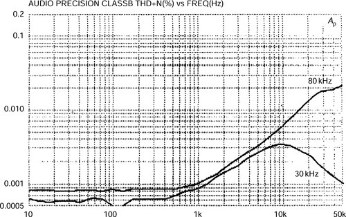
One should be cautious about any circuit arrangement which increases the NFB factor. Power amplifiers face loads that vary widely: it is difficult to be sure that a design will always be stable under all circumstances. This makes designers rather conservative about compensation, and I approached this technique with some trepidation. However, results were excellent with no obvious reduction in stability. Figure 7 shows the result of applying this technique to the Class B amplifier described below.
The simplest way to implement two pole compensation is shown in Figure 1(d), with typical values. Cp1 should have the same value as it would for stable single pole compensation, and CP2 should be at least twice as big; RP is usually in the region 1 k–10 k. At intermediate frequencies CP2 has an impedance comparable with Rp, and the resulting extra time constant causes the local feedback around the VAS to increase more rapidly with frequency, reducing the open loop gain at almost 12 dB/octave.
At HF the impedance of Rp is high compared with CP2, the gain slope asymptotes back to 6 dB/octave, and then operation is the same as conventional dominant pole, with Cdom equal to the series capacitance combination. So long as the slope returns to 6 dB/octave before the unity loop gain crossing occurs, there seems no obvious reason why the Nyquist stability should be impaired.
Figure 3 shows a simulated open loop gain plot for realistic component values; CP2 should be at least twice CP1 so the gain falls back to the 6 dB/octave line before the unity loop gain line is crossed. The potential feedback factor has been increased by more than 20 dB from 3 kHz to 30 kHz, a region where THD tends to increase due to falling NFB. The open loop gain peak at 8 kHz looks extremely dubious, but I have so far failed to detect any resulting ill effects in the closed loop behaviour.

There is however a snag to the simple approach shown here, which reduces the linearity improvement. Two-pole compensation may decrease open loop linearity at the same time as it raises the feedback factor that strives to correct it. At HF, CP2 has low impedance and allows Rp to directly load the VAS collector to ground. This worsens VAS linearity as we have seen. However, if CP2 and RP are correctly proportioned the overall reduction in distortion is dramatic and extremely valuable. When two pole compensation was added to Figure 4, the crossover glitches on the THD residual almost disappeared, being partially replaced by low level 2nd harmonic which almost certainly results from VAS loading. The positive slew rate will also be slightly reduced.
This looks like an attractive technique, as it can be simply applied to an existing design by adding two inexpensive components. If CP2 is much larger than CP1, then adding/removing Rp allows instant comparison between the two kinds of compensation. Be warned that if an amplifier is prone to HF parasitics then this kind of compensation may exacerbate them.
Design example: a 50 W class B amplifier
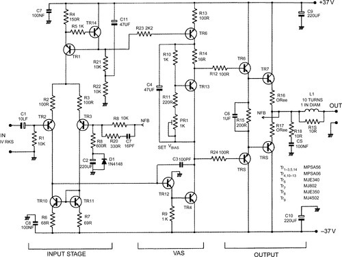
Figure 4 shows a design example of a Class B amplifier intended for domestic audio. Despite its conventional appearance, the circuit delivers a far better distortion performance than that normally associated with the arrangement.
With the supply voltages and values shown it delivers 50 W/8 Ω from IV r.m.s. input. In previous articles I have used the word blameless to describe amplifiers in which all distortion mechanisms, except the apparently unavoidable ones due to Class B, have been rendered negligible. This circuit has the potential to be blameless, but achieving this depends on care in cabling and layout. It does not aim to be a cookbook project; for example, overcurrent and DC offset protection are omitted.
The investigation presented in chapters 19 and 20 concluded that power fets were expensive, inefficient and non linear. Bipolars make good output devices. The best BJT configurations were the emitter follower type II, with least output switch-off distortion, and the complementary feedback pair (CFP) giving best basic linearity and quiescent stability.
I assume that domestic ambient temperatures will be benign, and the duty moderate, so that adequate quiescent stability can be attained by suitable heatsinking and thermal compensation. The configuration chosen is therefore emitter follower type II, which has the advantage of reducing switch-off nonlinearities (Distortion 3(c)) due to the action of R15 in reverse biasing the output base emitter junctions as they turn off. The disadvantage is that quiescent stability is worse than for the CFP output topology, as there is no local feedback loop to servo out Vbe variations in the hot output devices.
The NFB factor was chosen as 30 dB at 20 kHz, which should give generous HF stability margins. The input stage (current source Tr1, Tr14 and differential pair Tr2,3) is heavily degenerated by R2 R3 to delay the onset of third harmonic Distortion 1. To assist this the contribution of transistor internal re variation is minimised by using the unusually high tail current of 4 mA. Tr10,11 form a degenerated current mirror that enforces accurate balance of the Tr2,3 collector currents, preventing second harmonic distortion. Tail source Tr1,14 has a basic PSRR 10 dB better than the usual two diode version, though this is academic when C11 is fitted.
Input resistor R1 and feedback arm R8 are made equal and kept as low as possible consistent with a reasonably high input impedance, so that base current mismatch caused by beta variations will give a minimal DC offset. This does not affect Tr2-Tr3 Vbe mismatches, which appear directly at the output, but these are much smaller than the effects of Ib. Even if Tr2,3 are high voltage types with low beta, the output offset should be within ± 50 mV, which should be quite adequate, and eliminates balance presets and DC servos. A low value for R8 also gives a low value for R9, which improves the noise performance.
The value of C2 shown (220 μF) gives an LF roll off with R9 that is − 3 dB at 1.4 Hz. The aim is not an unreasonably extended sub-bass response, but to prevent an LF rise in distortion due to capacitor non linearity.
For example, 100 μF degraded the THD at 10 Hz from less than 0.0006% to 0.0011%. Band limiting should be done earlier, with non electrolytic capacitors. Protection diode D1 prevents damage to C2 if the amplifier suffers a fault that makes it saturate negatively; it looks unlikely but causes no measurable distortion.10 C7 provides some stabilising phase advance and limits the closed loop bandwidth; R20 prevents it upsetting Tr3.
The VAS stage is enhanced by an emitter follower inside the Miller compensation loop, so that the local NFB which linearises the VAS is increased by augmenting total VAS beta, rather than by increasing the collector impedance by cascoding. The extra local NFB effectively eliminates VAS nonlinearity (Distortion 2).
Increasing VAS beta like this presents a much lower collector impedance than a cascode stage due to the greater local feedback. The improvement appears to make a VAS buffer to eliminate Distortion 4 (loading of VAS collector by the nonlinear input impedance of the output stage) unnecessary. Cdom is relatively high at 100 pF, to swamp transistor internal capacitances and circuit strays, and make the design predictable. The slew rate calculates as 40 V/μsec. The VAS collector load is a standard current source, to avoid the uncertainties of bootstrapping.
Quiescent current stability
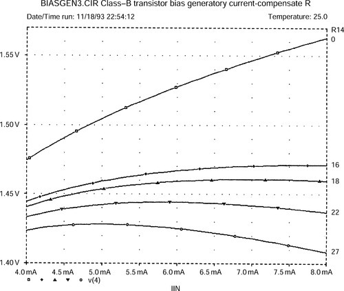
Since almost all the THD from a blameless amplifier is crossover, keeping the quiescent optimal is essential. Quiescent stability requires the bias generator to cancel out the Vbe variations of four junctions in series; those of two drivers and two output devices. Bias generator Tr13 is the standard Vbe multiplier, modified to make its voltage more stable against variations in the current through it. These occur because the biasing of Tr5 does not completely reject rail variations: its output current drifts initially due to heating thus changing its Vbe. Keeping a Class B quiescent stable is hard enough at the best of times, and so it makes sense to keep these extra factors out of the equation.
The basic Vbe multiplier has an incremental resistance of about 20 Ω; in other words its voltage changes by 1 mV for a 50 μA drift in standing current. Adding R14 converts this to a gently peaking characteristic that can be made perfectly flat at one chosen current; see Figure 5. Setting R14 to 22 Ω makes the voltage peak at 6 mA, and standing current now must deviate from this value by more than 500 μA for a 1 mV bias change. The R14 value needs to be altered if Tr5 is run at a different current. For example, 16 Ω makes the voltage peak at 8 mA instead. If TO3 outputs are used, the bias generator should be in contact with the top or can of one of the output devices, rather than the heatsink, as this is the fastest and least attenuated source for thermal feedback.
Output stage
The output stage is a standard double emitter follower apart from the connection of R15 between the driver emitters without connection to the output rail. This gives quicker and cleaner switch-off of the outputs at high frequencies; this may be significant from 10 kHz upwards dependent on transistor type. Speed up capacitor C5 improves the switch-off action. C6, R18 form the Zobel network while L1, damped by R19, isolates the amplifier from load capacitance.
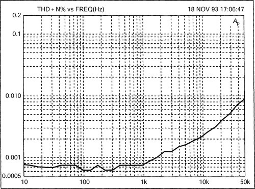
Figure 6 shows the 50 W/8 Ω distortion performance, about 0.001% at 1 kHz, and 0.006% at 10 kHz. The measurement bandwidth makes a big difference to the appearance, because what little distortion is present is crossover derived, and so high order. It rises at 6 dB/octave, the rate at which feedback factor falls. The crossover glitches emerge from the noise, like Grendel from the marsh, as the test frequency increases above 1 kHz. There is no precipitous THD rise in the ultrasonic region, and so I suppose this might be called a high speed amplifier.
Note that the zigzags on the LF end of the plot are measurement artifacts, apparently caused by the Audio Precision system trying to winkle distortion from visually pure white noise. Below 700 Hz the residual was pure noise with a level equivalent to approx 0.0006% at 30 kHz bandwidth. The actual THD here must be microscopic.
This performance can only be obtained if all seven of the distortion mechanisms are properly addressed; Distortions 1–4 are determined by the circuit design, but the remaining three depend critically on physical layout and grounding topology.
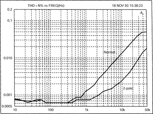
Figure 7 shows the startling results of applying two pole compensation to the amplifier. C3 remains 100 pF, while CP2 was 220 pF and RP 1kΩ. The extra NFB does its work extremely well, the 10 kHz THD dropping to 0.0015%, while the 1 kHz figure can only be guessed at. There were no unusual signs of instability on the bench, but I have not tried a wide range of loads.

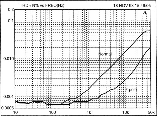
This experimental amplifier was rebuilt with three alternative output stages: the simple quasi-complementary, the quasi-Baxandall and the CFP. The results for both single and two pole compensation are shown in Figures 8, 9, and 10. The simple quasi-complementary generates more crossover distortion, as expected, and the quasi-Baxandall version is not a lot better, due to remaining asymmetry around the crossover region. The CFP gives even lower distortion than the original EF-II output. Figure 10 shows only the result for single pole compensation; in this case the improvement with two pole was marginal and the trace is omitted for clarity.
The AP plots in earlier parts of this series were mostly done with an amplifier similar to Figure 4, though of higher power. Main differences were the use of a cascode-VAS with a buffer, and a CFP output to minimise distracting quiescent variations. Measurements at powers above 100 W/8 Ω used a version with two paralleled output devices.