Distortion in power amplifiers, Part VIII: Class A amplifiers
There are two salient facts about Class A amplifiers: they are inefficient; they give the best possible distortion performance. The quiescent dissipation of the classic Class A amplifier is equal to twice the maximum output power, making massive output power impractical. But the nature of our hearing means that the power of an amplifier must be considerably increased to sound significantly louder. It is well known that power in watts must be quadrupled to double sound pressure level (SPL), but this is not the same as doubling subjective loudness; this is measured in Sones rather than dB above threshold, and some researchers have reported that doubling subjective loudness requires a 10 dB rather than 6 dB rise in SPL, implying that amplifier power must be increased tenfold, rather than merely quadrupled.1 This may help to put worries about amplifier size into perspective …
There is an attractive simplicity about class A. Most of the distortion mechanisms studied so far stem from class B, and we can thankfully forget crossover and switchoff phenomena (Distortions 3b, 3c), non-linear VAS loading, (Distortion 4) injection of supply-rail signals, (Distortion 5) induction from supply currents, (Distortion 6), and erroneous feedback connections. (Distortion 7) Beta-mismatch in the output devices can also be ignored.
The art of compromise
The only real disadvantage of class A is inefficiency, so inevitably efforts have been made to compromise between A and B. As compromises go, traditional class AB is not a happy one because, when the AB region is entered, the step change in gain generates significantly greater high order distortion than that from optimally biased class B. However, a well-designed AB amplifier will give pure class A performance below the AB threshold, something a class B amp cannot do.
Another compromise is the so-called non-switching amplifier, with its output devices clamped to pass a minimum current. However, it is not immediately obvious that a sudden halt in current-change as opposed to complete turn-off makes for a better crossover region. Those residual oscillograms that have been published seem to show that some kind of discontinuity still exists at crossover.2
A potential problem is the presence of maximum ripple on the supply rails at zero signal output; the PSRR must be taken seriously if good noise and ripple figures are to be obtained. This problem can be simply solved by the measures proposed for class B designs.
There is a kind of canonical sequence of efficiency improvement in class A amplifiers. The simplest kind is single-ended and resistively loaded, as at Figure 1(a). When it sinks output current, there is an inevitable voltage drop across the emitter resistance, limiting the negative output capability, and resulting in an efficiency of 12.5% (erroneously quoted in at least one textbook as 25%, apparently on the grounds that power not dissipated in silicon doesn’t count) This would be of purely theoretical interest – and not much of that – except that a single ended design has recently appeared. This reportedly produces a 10 W output for a dissipation of 120 W, with output swing predictably curtailed in one direction.3

A better method – constant current class A – is shown in Figure 1(b). The current sunk by the lower constant current source is no longer related to the voltage across it, and so the output voltage can approach the negative rail with a practicable quiescent current. (Hereafter shortened to ‘Iq’) Maximum efficiency is doubled to 25% at maximum output; for an example with 20 W output (and a big fan) see Ref. 4. Some versions (Krell) make the current source value switchable, controlling it with a kind of noise gate.
Push-pull operation once more doubles full-power efficiency, producing a more practical 50%; most commercial class A amplifiers have been of this type. Both output halves now swing from zero to twice the Iq , and least voltage corresponds with maximum current, reducing dissipation. There is also the intriguing prospect of cancelling the even-order harmonics generated by the output devices.
There are several ways to induce push-pull action. Figures 1(c), (d) show the lower constant current source replaced by a voltage controlled current source. This can be driven directly by the amplifier forward path, as in Figure 1(c),5 or by a current control negative feedback loop, as at Figure 1(d).6 The first of these methods has the drawback that the stage generates gain, phase splitter Tr1 doubling as the VAS; hence there is no circuit node that can be treated as the input to a unity gain output stage, making the circuit hard to analyse, as VAS distortion cannot be separated from output stage non-linearity. There is also no guarantee that upper and lower output devices will be driven appropriately for class A if the effective quiescent varies by more than 40% over the cycle.5
The second push-pull method in 1d is more dependable, and I can vouch that it works well. The disadvantage with the simple form shown is that a regulated supply is required to prevent rail ripple from disrupting the current loop control. Designs of this type have a limited current control range. In Figure 1(d), Tr3 cannot be turned on further once the upper device is fully off – so the voltage controlled current source will not be able to respond to an unforeseen increase in the output loading. If this happens there is no way of resorting to class AB to keep the show going and the amplifier will show some form of asymmetrical hard clipping.
The best push-pull stage seems to be that in Figure 1(e), which probably looks rather familiar. Like all the conventional class B stages examined in Chapter 19, this one will operate effectively in push-pull class A if the bias voltage is sufficiently increased; the increase over class B is typically 700 mV, dependant on the value of the emitter resistors. For an example of high biased class B see Ref. 7. This topology has the great advantage that, when confronted with an unexpectedly low load impedance, it will operate in class AB. The distortion performance will be inferior not only to class A but also to optimally biased class B, once above the AB transition level, but can still be made very low by proper design.
Although the push-pull concept has a maximum efficiency of 50%, this is only true at maximum sinewave output. Due to the high peak/average ratio of music, the true average efficiency probably does not exceed 10%, even at maximum volume before obvious clipping.
Other possibilities are signal controlled variation of the class A amplifier rail voltages, either by a separate class B amplifier, or a modulated switch mode supply. Both approaches are capable of high power output, but involve extensive extra circuitry, and present sent some daunting design problems.
A class B amplifier has a limited voltage output capability, but can be flexible about load impedances, as more current will be simply turned on when required. However, class A has also a current limitation, after which it enters class AB, and so loses its raison d’etre. The choice of quiescent value has a major effect on thermal design and parts cost so a clear idea of load impedance is important. The calculations to determine the required Iq are straightforward, though lengthy if supply ripple, Vce(sat), and Re losses, etc., are all considered, so I just give the results here. An unregulated supply with 10,000 μF reservoirs is assumed.
A 20 W/8 Ω amplifier will require rails of approx ± 24 V and a quiescent of 1.15A. If this is extended to give roughly the same voltage swing into 4 Ω, then the output power becomes 37 W, and to deliver this in class A the quiescent must increase to 2.16A, almost doubling dissipation. If however full voltage swing into 6 Ω will do, (which it will for many reputable speakers) then the quiescent only needs to increase to 1.5A; from here on I assume a quiescent of 1.6A to give a margin of safety.
The class A output stage
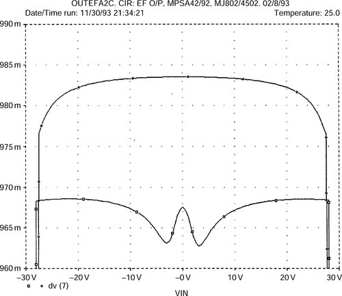
I consider here only the high biased class B topology, because it is probably the most popular approach, effectively solving the problems presented by the others. Figure 2 shows a Spice simulation of the collector currents in the output devices versus output voltage for the emitter follower configuration, and also the sum of these currents. This sum of device currents is, in principle, constant, but need not be so for low THD. The output signal is the difference of device currents and is not inherently related to the sum. However, a large deviation from this constant sum condition means inefficiency, as the stage is conducting more quiescent than it needs to for some part of the cycle. The constancy of this sum is important because it shows that the voltage measured across Re1 and Re2 together is also effectively constant so long as the amplifier stays in class A. This in turn means that Iq can be simply set with a constant voltage bias generator, in very much the same way as class B.

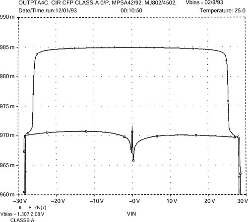
Figures 3, 4, 5 show Spice gain plots for open loop output stages, with 8 Ω loading and 1.6 A quiescent; the circuitry is exactly as for class B in Part 4. The upper traces show class A gain, and the lower traces gain under optimal class B bias for comparison. Figure 3 shows an emitter follower output, Figure 4(a) simple quasi complementary stage, and Figure 5(a) CFP output.

We would expect class A stages to be more linear than B, and they are Harmonic and THD figures for the three configurations, at 20 V peak, are shown in Table 1. There is absolutely no gain wobble around OV, and push-pull class A genuinely does cancel even order distortion. Class B only does this in the crossover region, in a partial and unsatisfactory way.
Table 1
| Harmonic | Emitter Follower (%) | Quasi-Comp (%) | CFP Output (%) |
| Second | 0.00012 | 0.0118 | 0.00095 |
| Third | 0.0095 | 0.0064 | 0.0025 |
| Fourth | 0.00006 | 0.0011 | 0.00012 |
| Fifth | 0.00080 | 0.00058 | 0.00029 |
| THD | 0.0095 | 0.0135 | 0.0027 |

THD is calculated from the first nine harmonics, though levels above the fifth are very small
It is immediately clear that the emitter follower has more gain variation, and therefore worse linearity, than the CFP, while the quasi complementary circuit shows an interesting mix of the two. The more curved side of the quasi gain plot is on the negative side, where the CFP half of the quasi circuit is passing most of the current. However we know by comparing Figure 3 and Figure 5 that the CFP is the more linear structure. Therefore it appears that the shape of the gain curve is determined by the output half that is turning off, presumably because this shows the biggest gm changes. The CFP structure maintains gm better as current decreases, and so gives a flatter gain curve with less rounding of the extremes.
The gain behaviour of these stages is reflected in their harmonic generation; Table 1 reveals that the two symmetrical topologies give mostly odd order harmonics as expected. The asymmetry of the quasi comp version causes a large increase in even order harmonics, and this is reflected in the higher THD figure. Nonetheless the THD figures are still two to three times lower than for their class B equivalents.
If this factor of improvement seems a poor return for the extra dissipation of class A, this is not so. The crucial point about the distortion from a class A output stage is not just that is low, but that it is low order, and so benefits much more from a typical NFB factor that falls with frequency than does high order crossover distortion.
The choice of class A output topology is now simple. For best performance, use the CFP. Apart from greater basic linearity, the effects of output device temperature on Iq are servoed out by local feedback, as in class B. For utmost economy, use the quasi complementary with two NPN devices: these need only a low Vce(max) for a typical class A amp, so here is an opportunity to recoup some of the money spent on heatsinking.
The rules are different from class B; the simple quasi configuration will give first class results with moderate NFB, and adding a Baxandall diode to simulate a complementary emitter follower stage makes little difference to linearity.7
It is sometimes assumed that the different mode of operation of class A makes it inherently short circuit proof. This may be true with some configurations, but the high biased type shown here will continue delivering current until it bursts. Overload protection is no less necessary.
Quiescent control systems
Unlike class B, precise control of quiescent current is not required to optimise distortion. For good linearity there just has to be enough of it. However, Iq must be under some control to prevent thermal runaway, particularly if the emitter follower output is used, and an ill conceived controller can ruin the THD. There is also the point that a precisely held standing current is considered the mark of a well bred class A amplifier; a quiescent that lurches around like a drunken sailor does not inspire confidence.
Thermal feedback from the output stage to a standard Vbe multiplier bias generator will work,8 and should be sufficient to prevent run-away. However, unlike class B, class A gives the opportunity of tightly controlling Iq by negative feedback. This is profoundly ironic because now that we can precisely control Iq, it is no longer critical. Nevertheless it seems churlish to ignore the opportunity.
There are two basic methods of feedback current control. In the first, the current in one output device is monitored, either by measuring the voltage across one emitter resistor, (Rs in Figure 6(a)), or by a collector sensing resistor. The second method monitors the sum of the device currents, which as described above, is constant in class A.

The first method as implemented in Figure 6(a)7 compares the Vbe of Tr4 with the voltage across Rs , with filtering by RF, CF. If quiescent is excessive, then Tr4 conducts more, turning on Tr5 and reducing the bias voltage between points A and B.
In Figure 6(b), which uses the voltage controlled current source approach, the voltage across collector sensing resistor Rs is compared with Vref by Tr4, the value of Vref being chosen to allow for Tr4 Vbe.9 Filtering is once more by RF, CF.
For either Figure 6(a) or 6(b), the current being monitored contains large amounts of signal, and must be low pass filtered before being used for control purposes. This is awkward as it adds one more time constant to worry about if the amplifier is driven into asymmetrical clipping, and implies the desirability of large electrolytic capacitors to minimise the a.c. voltage drop across the sense resistors. In the case of collector sensing there are unavoidable losses in the extra sense resistor. It is my experience that imperfect filtering can produce a serious rise in distortion.
The better way is to monitor current in both emitter resistors. As explained above, the voltage across both is very nearly constant, and in practice filtering is unnecessary. An example of this approach is shown in Figure 6(c), based on a concept originated by Nelson Pass.10 Here Tr4 compares its own Vbe with the voltage between X and B; excessive quiescent turns on Tr4 and reduces the bias directly. Diode D is not essential to the concept, but usefully increases the current feedback loop gain; omitting it more than doubles Iq variation with Tr7 temperature in the Pass circuit.
The trouble with this method is that Tr3 Vbe directly affects the bias setting, but is outside the current control loop. A multiple of Vbe is established between X and B, when what we really want to control is the voltage between X and Y. The temperature variations of Tr4 and Tr3 Vbe partly cancel, but only partly. This method is best used with a CFP or quasi output so that the difference between Y and B depends only on the driver temperature, which can be kept low. The ‘reference’ is Tr4 Vbe, which is itself temperature dependent. Even if it is kept away from the hot bits it will react to ambient temperature changes, and this explains the poor performance of the Pass method for global temperature changes (Table 2).
Table 2
Iq change per °C change in temperature
| Changing Tr7 temperature only | Changing Global temperature (%) | |
| Quasi + Vbe mult | + 0.112% | − 0.43 |
| Pass: as Flg. 6c | + 0.0257 | − 14.1 |
| Pass: no dlode D | + 0.0675 | − 10.7 |
| New system: | + 0.006% | − 0.038 |
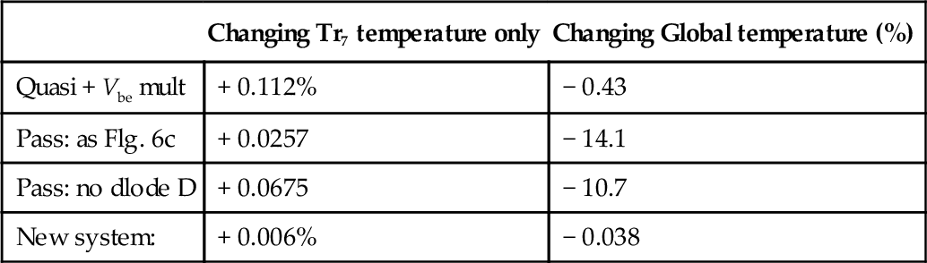
(assuming 0.22 Ω emitter resistors and 1.6A Iq.)
To solve this problem, I would like to introduce the novel control method in Figure 7. We need to compare the floating voltage between X and Y with a fixed reference, which sounds like a requirement for two differential amplifiers. This can be reduced to one by sitting the reference Vref on point Y. This is a very low impedance point and can easily swallow a reference current of 1 mA or so. A simple differential pair Tr15,16 then compares the reference voltage with that at point X: excess quiescent turns on Tr16, causing Tr13 to conduct more and reducing the bias voltage.
The circuitry looks enigmatic because of the high impedance of Tr13 collector would seem to prevent signal from reaching the upper half of the output stage; this is in essence true, but the vital point is that Tr13 is part of a NFB loop that establishes a voltage at A that will keep the bias voltage between A and B constant. This comes to the same thing as maintaining a constant Vbias across Tr13. As might be imagined, this loop does not shine at transferring signals quickly, and this duty is done by feedforward capacitor C4.
Without it, the loop (rather surprisingly) works correctly, but HF oscillation at some part of the cycle is almost certain. With C4 in place the current loop does not need to move quickly, since it is not required to transfer signal but rather to maintain a DC level.
The experimental study of Iq stability is not easy because of the inaccessibility of junction temperatures. Professional Spice implementations like PSpice allow both the global circuit temperature and the temperature of individual devices to be manipulated; this is another aspect where simulators shine. The exact relationships of component temperatures in an amplifier is hard to predict: I show here just the results of changing the global temperature of all devices, and changing the junction temp of Tr7 alone (Figure 7) with different current controllers. Tr7 will be one of the hottest transistors and unlike Tr9 it is not in a local NFB loop, which would greatly reduce its thermal effects.
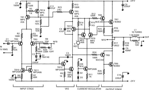
A new class A design
The full circuit diagram shows a ‘blameless’ 20 W/8 Ω class A power amplifier. This is as close as possible in operating parameters to the previous class B design to aid comparison. In particular the NFB factor remains 30 dB at 20 kHz. The front end is as for the class B version, which should not be surprising as it does exactly same job, input Distortion 1 being unaffected by output topology.
As before the input pair uses a high tail current, so that R2,3 can be introduced to linearise the transfer characteristic and set the transconductance. Distortion 2 (VAS) is dealt with as before, the beta enhancer Tr12 increasing the local feedback through Cdom. There is no need to worry about Distortion 4 (non-linear loading by output stage) as the input impedance of a class A output, while not constant, does not have the sharp variations shown by class B.
The circuit uses a standard quasi output. This may be replaced by a CFP stage without problems. In both cases the distortion is extremely low but, gratifyingly, the CFP proves even better than the quasi, confirming the simulation results for output stages in isolation.
The operation of the current regulator Tr13,15,16 has already-been described. Using a band gap reference, it holds a 1.6 A Iq to with in ± 2 mA from a second or two after switch on. Looking at Table 2, there seems no doubt that the new system is effective.
As before an unregulated power supply with 10,000 μF reservoirs was used, and despite the higher prevailing ripple, no PSRR difficulties were encountered once the usual decoupling precautions were taken.
Performance
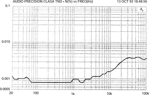
The closed loop distortion performance (with conventional compensation) is shown in Figure 8 for the quasi comp output stage, and in Figure 9 for a CFP output version. The THD residual is pure noise for almost all of the audio spectrum, and only above 10 kHz do small amounts of third harmonic appear. The suspected source is the input pair, but this so far remains unconfirmed.
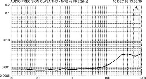
The distortion generated by the class B and A design examples is summarised in Table 3, which shows a pleasing reduction as various measures are taken to deal with it. As a final tweak, two pole compensation was applied to the most linear (CFP) of the class A versions, reducing distortion to 0.0012% at 20 kHz, at some cost in slew rate (Figure 10). While this may not be the fabled straight wire with gain, it must be a near relation …
Table 3
| 1 kHz | 10 kHz | 20 kHz | Power | |
| class B EF | < .0006% | .0060% | .012% | 50 W |
| class B CFP | < .0006% | .0022% | .0040% | 50 W |
| class B EF 2-pole | < .0006% | .0015% | .0026% | 50 W |
| class A quasl | < .0006% | .0017% | .0030% | 50 W |
| class A CFP | < .0006% | .0010% | .0018% | 20 W |
| class A CFP 2-pole | < .0006% | .0010% | .0012% | 20 W |
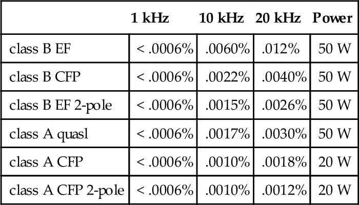
(All for 8 Ω loads and 80 kHz bandwidth. Single pole compensation unless otherwise stated.)

And finally
The techniques in this series have a relevance beyond power amplifiers. Applications obviously include discrete op-amp based preamplifiers11 and extend to any amplifier offering static or dynamic precision. My philosophy is that all distortion is bad, and high order distortion is worse … n2/4 worse, according to many authorities12 Digital audio routinely delivers the signal with less than 0.002% THD, and I can earnestly vouch for the fact that analogue console designers work hard to keep the distortion in long and complex signal paths down to similar levels. I think it an insult to allow the very last piece of electronics in the chain to make nonsense of these efforts.
I do not believe that an amplifier yielding 0.001% THD is going to sound much better than another generating 0.002%. However, if there is ever a doubt as to what level of distortion is perceptible, then using the techniques I have presented, it should be possible to reduce the THD below the level at which there can be any rational argument.
I am painfully aware of the school of thought that regards low distortion as inherently immoral, but this is to confuse electronics with religion. The implication is that very low THD can only be obtained by huge global NFB factors which in turn require heavy dominant pole compensation that severely degrades slew rate. The obvious flaw in this argument is that, once the compensation is applied, the amplifier no longer has a large global NFB factor: Its distortion performance presumably reverts to mediocrity, further burdened with a slew rate of 4 V per fortnight.
To me low distortion has its own aesthetic appeal. All of the linearity enhancing strategies examined in this series are of minimal incremental cost to existing designs with the possible exception of using class A. There seems to be no reason to not use them.