Load-invariant audio power
It has been my experience that power amplifiers always, without exception, give more distortion with heavier loading i.e., with a lower load impedance. This, in BJT amplifiers at least, is due to an extra distortion mechanism that becomes more and more important as the load impedance falls and the output stage currents increase. Against all intuition, the source of the increased distortion is the drivers, and not the output devices themselves; this was wholly unexpected, and to the best of my knowledge was a new discovery. It was uncovered not so much by mathematics or theory as by some careful SPICE analysis, later backed up by measurements, and was a copybook example of just how very powerful and useful circuit simulation can be in the right circumstances.
To see if this extra distortion could be eliminated, or at any rate reduced with respect to its ‘normal’ levels, I conducted a little research program, and this chapter was the result. It was not possible to make the amplifier totally Load-Invariant, i.e., with the same THD at 4 Ω as 8 Ω, but I think I got pretty close.
My investigations into power amplifiers have so far largely concentrated on 8 Ω resistive loading. This is open to criticism, as loudspeaker impedance dips to 4 Ω or less are not uncommon. Solid-state amplifiers always give more distortion with heavier loading, without exception so far as I am aware.
While it would be highly desirable from the amplifier designer’s point of view for the loudspeaker designer to strive for a reasonably flat impedance, it has to be accepted that electronic problems are much easier to solve than electromechanical ones. It follows that it is reasonable for amplifiers to accommodate themselves to loudspeakers rather than the other way around. Thus an amplifier must be able to cope gracefully with impedance dips to 4 Ω or lower.
Such dips tend to be localised in frequency, so music does not often dwell in them. An amplifier should be capable of driving half the nominal load impedance at almost the full voltage swing, though not necessarily for more than a minute or so.
Contemporary power amplifier ratings tend to be presented in the format ‘X watts into 8 Ω, Y watts into 4 Ω’ from which we presumably may deduce:
• The amplifier will deliver sustained power into 4 Ω.
• Since 2 Ω loads are not explicitly mentioned, they cannot be driven in a sustained fashion.
It may also be assumed, but with much less certainty, that,
• The amplifier will cope with short-term 2 Ω impedance dips; i.e. half the lowest nominal load quoted.
• The overload protection – if it exists at all – activates below 2 Ω. Note that no minimum load impedance is specified.
Output loading and distortion
A ‘Blameless’ Class-B power amplifier is one wherein all the distortion mechanisms shown in Table 1 have been eliminated or reduced to below the noise floor, except for the intractable Distortion 3 in its three subcategories. I have produced a slim monograph which describes the philosophy and practicalities of this in greater detail than EW articles permit.1
Table 1
Characteristics of distortion mechanisms.
| No. | Mechanism | Category | Component sensitive? |
| 1 | Input Vin/Iout nonlinearity | Inherent | No |
| 2 | VAS Iin/Vout nonlinearity | Inherent | Yes? |
| 3 | Output stage distortions: | ||
| a) Large-signal nonlinearity | Inherent | Yes | |
| b) Crossover distortion | Inherent | No? | |
| c) Switch-off distortion | Inherent | Yes | |
| 4 | Non-linear voltage-amplifier stage loading | Inherent | Yes |
| 5 | Rail decouple grounding | Topological | No |
| 6 | Rail current induction | Topological | No |
| 7 | Error in negative-feedback take-off-point | Topological | No |
| 8 | Feedback cap distortion | Inherent | Yes |
A Blameless design gives a distortion performance into 8 Ω that depends very little on variable transistor characteristics such as beta. This is because at this load impedance the output stage nonlinearity is almost all crossover distortion, which is primarily a voltage-domain effect.
Note that for optimal crossover behaviour the quantity to be set is Vq, the voltage across the two output emitter resistors Re, and the actual value of the resulting Iq is incidental.2 Mercifully, in Class-B the same Vq remains optimal whatever the load impedance; if it did not the extra complications would be serious.
As the load impedance of a Blameless Class-B amplifier is decreased from infinite to 4 Ω, distortion increases in an intriguing manner. Unloaded, the THD is not much greater than that from the Audio Precision test oscillator, but with loading crossover distortion increases steadily, Figure 1.

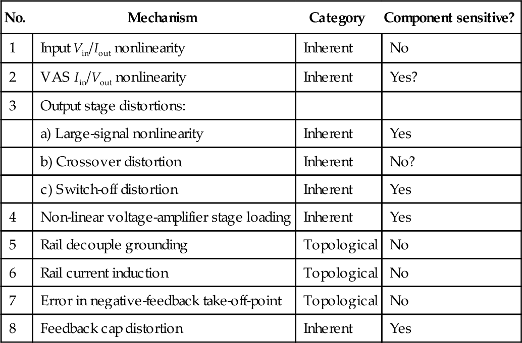
When the load impedance falls below about 8 Ω, a new distortion begins to appear, overlaid on the existing crossover nonlinearities. It is low-order, and essentially third-harmonic. In Figure 2 the upper 4 Ω THD trace is consistently twice that for 8 Ω, once it clears the noise floor.

In Chapter 20, I labelled this as Distortion 3a, or large signal nonlinearity. The word ‘large’ refers to currents rather than voltages. Unlike crossover distortion 3b, the amount of LSN produced is significantly dependant on device characteristics.3 The distortion residual is essentially third-order due to the symmetric and compressive nature of the output stage gain characteristic, but its appearance on a scope can be complicated by different amounts of nonlinearity in the upper and lower output stage halves.
Large signal nonlinearity occurs in both emitter-follower and complementary feedback pair output configurations; this chapter concentrates on the complementary feedback pair, as in Figure 3. Incremental gain of a simulated complementary feedback pair output stage for 8 and 4 Ω is shown in Figure 4; the lower 4 Ω trace has greater downward curvature, i.e. a greater fall off of gain with increasing current. Simulated emitter follower behaviour is similar.

As it happens, an 8 Ω nominal impedance is a pretty good match for standard power bipolar junction transistors, though 16 Ω might be better for minimising large-signal nonlinearity – loudspeaker technology permitting. It is presumably coincidental that the 8 Ω nominal impedance corresponds approximately with the heaviest load that can be driven without large signal nonlinearity appearing.
Since large signal nonlinearity is an extra distortion component laid on top of others, and usually dominating them in amplitude, it is obviously simplest to minimise the 8 Ω distortion first, so that 4 Ω effects can be seen more or less in isolation when they appear.
The typical result of 4 Ω amplifier loading was shown in Figure 2, for the relatively modern MJ15024/25 complementary pair from Motorola. Figure 5 shows the same for one of the oldest silicon complementary pairs, the 2 N3055/2955, unfortunately on a slightly different frequency scale. The 8 Ω distortion is similar for the different devices, but the 4 Ω THD is 3.0 times worse for the venerable 2 N3055/2955. Such is progress.

Such experiments with different output devices throw useful light on the Blameless concept. From various types tried so far it can be said that Blameless performance, independent of output device type, should not exceed 0.001% at 1 kHz and 0.006% at 10 kHz, into 8 Ω. All the components existed to build sub-0.001% THD amplifiers in mid-1969 – if only we had known how to do it.
Low-impedance loads have other implications beyond worsening the THD. The requirements for long-term 4 Ω operation are severe, demanding significantly more heatsinking and power supply capacity if reliability is to be maintained.
For economic reasons the peak–average ratio of music is usually fully exploited, though this can cause real problems on extended tests, such as the FTC 40%-power-for-an-hour preconditioning procedure.
The main subject of this article is the extra distortion generated in the output stage itself by increased loading, but there are other ways in which the total amplifier distortion may be degraded by the increased currents flowing.
Table 1 shows the main distortion mechanisms in a power amplifier; Distortions 1, 2, and 8 are unaffected by output stage conditions. Distortion 4 might be expected to increase, as the increased loading on the output stage is reflected in increased voltage amplifier stage loading.4 However, both the beta-enhanced emitter-follower and buffered-cascode methods seem to cope effectively with sub-8 Ω loads.
The greater supply currents drawn could increase the rail ripple, which will worsen Distortion 5 if it exists. But since the supply reservoir capacitance must also be increased to permit greater power delivery, ripple will be reduced again and this tends to cancel out. If the rail ripple does increase, the usual RC filtering of bias supplies5 deals with it effectively, preventing it getting in via the input pair tail, etc.
Distortion 6 may be more difficult to eliminate as the halfwave currents flowing in the output circuitry are twice as large, with no counteracting mechanism. Distortion 7, if present, will be worsened due the increased load currents flowing in the output stage wiring resistances.
Of those mechanisms above, Distortion 4 is inherent in the circuit configuration – though not a problem in practice – while 5, 6, and 7 are topological, in that they depend on the spatial and geometrical arrangements of components and wiring. The latter three can therefore be completely eliminated in both theory and practice. This leaves us with only the large signal nonlinearity component of Distortion 3 to grapple with.
The load-invariant concept
Ideally, the extra distortion component large signal nonlinearity would not exist. Such an amplifier would give no more distortion into 4 Ω than 8, and I call it ‘load-invariant to 4 Ω’. The loading qualification is required because, as you will see, the lower the impedance, the greater the difficulties in aspiring to load-invariance.
I am assuming that we start out with an amplifier that is Blameless at 8 Ω; it would be logical but pointless to apply the term ‘load-invariant’ to an ill-conceived amplifier delivering 1% THD into both 8 and 4 Ω.
Large signal nonlinearity
Large signal nonlinearity is clearly a current-domain effect, dependent on the magnitude of the signal currents flowing in drivers and output devices, as the voltage conditions are unchanged.
A 4 Ω load doubles the output device currents, but this does not in itself generate significant extra distortion. The crucial factor appears to be that the current drawn from the drivers by the output device bases more than doubles, due to beta fall-off in the output devices with increasing collector current. It is this extra increase of current due to beta-droop that causes almost all the additional distortion.
The exact details of how this works are not completely clear, but seems to be because the ‘extra current’ due to beta fall-off varies very non linearly with output voltage. It appears that the non linear extra current combines with driver nonlinearity in a particularly pernicious way. Beta-droop is ultimately due to what are called high-level injection effects. These vary with device type, so device characteristics now matter.
As I stated in my original power-amplifier series,6 there is good simulator evidence that large signal nonlinearity is entirely due to the beta-droop causing extra current to be drawn from the drivers. To recapitulate:
• Simulated output stages built from output devices modified to have no beta-droop (by increasing Spice model parameter IKF) have no large signal nonlinearity. It seems to be specifically the extra current taken due to beta-droop that causes the trouble.
• Simulated output devices driven with zero-impedance voltage sources instead of transistor drivers show no large signal nonlinearity. This shows that such nonlinearity does not occur in the outputs themselves, but in the driver transistors.
• Output stage distortion can be regarded as an error voltage between input and output. The double emitter-follower emitter-follower stage error is driver Vbe + output Vbe + Re drop. A simulated emitter-follower output stage with the usual drivers shows that it is primarily nonlinearity in the driver Vbe that increases as the load resistance reduces, rather than in the output Vbe. The drop across Re is essentially linear.
These three results have naturally been rechecked for this article.
Knowing that beta-droop caused by increased output device Ic is at the root of the problem leads to some solutions. Firstly, the per-device Ic can be reduced by using parallel output devices. Alternatively Ic can be left unchanged and output device types selected for the least beta droop.
Feedforward diodes across the emitter resistors sometimes help, but they treat the symptoms – by attempting distortion cancellation – rather the root cause, so it is not surprising this method is much less effective.
Doubled output devices
The basic philosophy here, indicated above, is that the output devices are doubled even though this is quite unnecessary for handling the power output required.
The fall-off of beta depends on collector current. If two output devices are connected in parallel, the collector current divides in two between them, and beta-droop is much reduced. From the above evidence, I predicted that this ought to reduce large-signal nonlinearity and when measured, indeed it does.
This sort of reality-check must never be neglected when you are using simulations. Figure 6 compares 4 Ω THD at 60W for single and doubled output devices, showing that doubling reduces distortion by about 1.9 times; well worthwhile. The output transistors were standard power devices, in this case Motorola MJ15024/15025.

The 2 N3055/2955 complementary pair give a similar halving of large-signal nonlinearity on being doubled, though the initial distortion is three times higher into 4 Ω. Those 2N3055s with an H suffix are markedly worse than those without.
No current-sharing precautions were taken when doubling the devices, and this lack seemed to have no effect on large-signal nonlinearity reduction. There was no evidence of current-hogging.
Doubling the power devices naturally increases the power output capability, though if this is fully exploited large-signal nonlinearity will tend to rise again, and you are back where you started. It will also be necessary to uprate the power supply and so on. The essence of this technique is to use parallel devices to reduce distortion long before power handling alone compels you to do so.
Better output devices
The TO3P-packaged 2SC3281 and 2SA1302 complementary pair has a reputation in the hi-fi world for being ‘more linear’ than the run of transistors. This is the sort of vague claim that arouses the deepest of suspicions, and is comparable with the many assertions of superior linearity in power fets, which is the exact opposite of reality.7
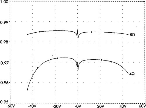
In this case however, the kernel of truth is that the 2SC3281 and 2SA1302 show much less beta-droop than average power transistors. These devices were introduced by Toshiba; Motorola versions are MJL3281A and MJL1302A, also in TO3P. Figure 7 shows beta-droop, for the various devices discussed here, and it is clear that more droop means more large-signal nonlinearity.
The 3281/1302 pair is clearly in a different class from more conventional transistors as regards maintenance of beta with increasing collector current. There seems to be no special name for this class of bipolar junction transistors, so I have called them ‘sustained-beta’ devices here.
Into 4 and 8 Ω, the THD for single 3281/1302 devices is shown in Figure 8. Distortion is reduced by about 1.4 times compared with the standard devices of Figure 2, over 2–8 kHz. Several pairs of 3281/1302 have been tested and the 4 Ω improvement is consistent and repeatable.

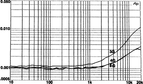
The obvious next step is to combine the two techniques by using double sustained-beta devices. Doubled device results are shown in Figure 9 where the distortion at 80W/4 Ω (15 kHz) is reduced from 0.009% in Figure 8 to 0.0045% – in other words halved. The 8 and 4 Ω traces are now very close, the 4 Ω THD being only 1.2 times higher than the 8 Ω case.

Some similar devices exist. Other devices showing less beta-droop than standard are MJ21193, MJ21194, in TO3 packaging, and MJL21193, MJL21194 in TO3P, also from Motorola. These devices show beta-maintenance intermediate between the ‘super’ 3281/1302 and ‘ordinary’ MJ15024/25, so it seemed likely that they would give less large-signal nonlinearity than ordinary power devices, but more than the 3281/1302. This prediction was happily fulfilled.
It could be argued that multiplying output transistors is an expensive way to solve a problem. To give this perspective, in a typical stereo power amplifier, including heatsink, metal work and mains transformer, doubling the output devices will only increase the total cost by about 5%.
Feeding forward
In the Distortion in Power Amplifiers series, the only technique I could offer for improving large-signal nonlinearity was the use of power diodes across 0.22 Ω output emitter resistors.8 The improvement was only significant for high power into less-than 3 Ω loading, and was of doubtful utility for hifi.
It is now my practice to make output emitter resistors Re 0.1 Ω, rather than the more usual 0.22 Ω. This both improves voltage-swing efficiency and reduces the extra distortion generated if the amplifier is erroneously biased into Class AB.8 Thus even with low-impedance loads the Re voltage drop is very small, and insufficient to turn on a silicon power diode at realistic output levels.
Schottky diodes have a much lower forward voltage drop and might be useful here. Tests with 50 A diodes have been made but have so far not been encouraging in the distortion reduction achieved. A suitable Schottky diode costs at least as much as an output transistor, and two will be needed.
The trouble with triples
In electronics, there is often a choice between applying brawn – in this case using multiple power devices – or brains to solve a given problem. The ‘brains’ option would be represented by a clever circuit configuration that gave the same results without replication of expensive power silicon.
The obvious place to start looking is the various output-triple topologies that have occasionally been used. Note that ‘output-triples’ here refers to pre-driver, driver, and output device all in a local negative-feedback loop, rather than three identical output devices in parallel, which I would call ‘tripled outputs’. Nomenclature is a problem.
In simulation, output-triple configurations do indeed reduce the gain-droop that causes large-signal nonlinearity. There are many different ways to configure output-triples. They vary in their general linearity and effectiveness at minimising large-signal nonlinearity.
The real difficulty with this approach is that three transistors in a local loop are very prone to parasitic and local oscillations. This is exacerbated by reducing the load impedances, presumably because the higher collector currents lead to increased device transconductance. This sort of problem can be very hard to deal with, and in some configurations appears almost insoluble. I have not studied this approach further.
Loads below 4 Ω
So far I have concentrated on 4 Ω loads; loudspeaker impedances can sink lower than this, so I pursued the matter down to 3 Ω. One pair of 3281/1302 devices will deliver 50W into 3 Ω for THD of 0.006% at 10 kHz, Figure 10. Two pairs of 3281/1302s reduce this to 0.003% at 10 kHz, Figure 11. This is a very good result for such simple circuitry, and may be something of a record for 3 Ω linearity.

At this point it seems that whatever the device type, doubling the outputs halves the THD percentage for 4 Ω loading. The principle can be extended down to 2 Ω operation, but tripled devices are required for sustained operation at significant powers. Resistive losses are serious, so 2 Ω power output may be little greater than that into 4 Ω.
Improved 8 Ω performance
It was wholly unexpected that the sustained-beta devices would also show lower crossover distortion at 8 Ω – but they do. What is more, the effect is again repeatable.
Possibly, whatever improves the beta characteristics has also somewhat altered the turn-on law so that crossover distortion is reduced; alternatively traces of large-signal nonlinearity, not visible in the THD residual, may have been eliminated.
Plot Figure 11 shows the improvement over the MJ15024/25 pair; the 8 Ω THD at 10 kHz is reduced from 0.003% to 0.002%, and with correct bias adjustment, crossover artifacts are simply not visible on the 1 kHz THD residual.
The artifacts are only just visible in the 4 Ω case. To get a feel for the distortion being produced, and to set the bias optimally, it is necessary to test at 5 kHz into 4 Ω.
Implementing the load-invariant concept
Figure 12 shows the circuit of a practical load-invariant amplifier intended for 8 Ω nominal loads with 4 Ω impedance dips. Its distortion performance is shown in Figures 6–11, depending on the output devices fitted.

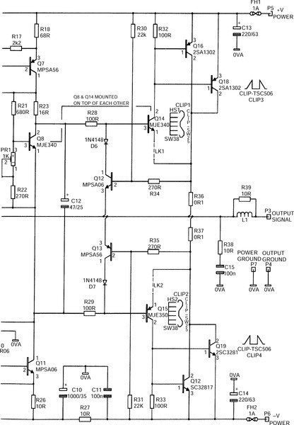
Apart from load-invariance, this design also incorporates two new techniques from the thermal dynamics series.
The first technique greatly reduces time-lag in the thermal compensation. With a complementary-feedback pair output stage, the bias generator aims to shadow driver junction temperature rather than the outputs. A much faster response to power dissipation changes is obtained by mounting the bias generator transistor Tr8 on top of driver Tr14, rather than on the other side of the heat-sink. Driver heat-sink mass is thus largely decoupled from the thermal compensation system, speeding up the response by at least two orders of magnitude.9
The second new technique is the use of a bias generator with an increased temperature coefficient, to reduce the static errors introduced by thermal losses between the driver and the sensor. Temperature coefficient is increased to − 4.0 mV/°C.10 Diode D5 also compensates for the effect of ambient temperature changes.
The design is not described in detail because much of it closely follows the Blameless Class-B amplifier described Refs 1 and 11. Some features are derived from the Trimodal amplifier.8 Most notable of these is the low-noise feedback network, with its requirement for input boot-strapping if a 10 kΩ input impedance is required. Single-slope VI limiting is incorporated for overload protection; see Tr12,13.
As usual the global negative feedback factor is a modest 30 dB at 20 kHz.
A point of departure
The improvements described here fit neatly into the philosophy of Blameless power amplifiers. The fundamental principle of the Blameless concept is that Distortion 3 should be the only significant distortion remaining. Distortions 1, 2 and 4–8 can all be reduced to negligible levels in straight-forward ways.
For 8 Ω operation, the main nonlinearity left is crossover distortion, which seems to vary only very slightly with output transistor type.
As I hoped, the concept of a Blameless power amplifier is proving extremely useful as a defined point of departure for new amplifier techniques. Starting from the standard Blameless Class-B amplifier, I have derived:
• The pure Class-A power amplifier12
• The Trimodal A/AB/B amplifier8
• The load-invariant amplifier described here
• A further new design to be announced.
Note that Trimodal and new load-invariant amplifier are simple add-ons to the basic Blameless Class-B configuration. The Trimodal design adds a Class-A biasing subsystem, and the new amplifier grafts on extra – or improved – output devices.
In summary
This study is incomplete in that the details of the large-signal nonlinearity mechanism remain incompletely understood, even though several practical methods for reducing it now exist. A detailed mathematical analysis would probably get to the bottom of it, but a foot-long equation usually gives little physical insight.
My initial thoughts were that an amplifier could be considered as load-invariant if the rise in THD from 8 Ω to 4 Ω was less than some given ratio. For normal amplifiers the THD increase factor is from two to three times. The actual figure attained by the amplifier presented here is 1.2 times. I, for one, am prepared to classify this as ‘load-invariant’. The ratio could probably be made even closer to unity by tripling the outputs.
Remember that this amplifier is designed for 8 Ω nominal loads, and their accompanying impedance dips; it is not intended for speakers that start out at 4 Ω nominal and plummet from there. Nonetheless, I hope it is some progress towards load-invariance, and that power amplifier design might have taken another small step forward.