4 Fabrication of Multiple-Quantum Dots (MQDs) by MLD
Multiple quantum dot (MQD) in polymer wires is one of the distinguished structures accomplished by molecular layer deposition (MLD).
In the present chapter, experimental demonstrations of the MQD construction are presented.
4.1 Fundamentals of Quantum Dots
Control of dimensionality is an important issue to improve various kinds of optical and electronic properties of materials. Figure 4.1 shows a schematic illustration of three-, two-, one-, and zero-dimensional systems, which respectively correspond to bulks, quantum wells, quantum wires, and quantum dots. The dimensionality of materials affects energy dependence of the density of states [1], which gives rise to variations of optical and electronic properties.
Figure 4.2 shows shell shapes for given energy of a free electron in three-, two-, and one-dimensional systems. Here, k represents the wavenumber. In the three-dimensional system, the shell is a spherical surface with a radius of k and a thickness of dk. In the two-dimensional system, the shell is a circle with a radius of k and a thickness of dk, and in the one-dimensional system, the shell is two short lines with a length of dk.
From these shell shapes, density of states can be calculated based on the free-electron model, where wavefunctions and energy of electrons are expressed as
Here, k is the wavenumber vector, m is the mass of an electron, and L3 is the volume where electrons exist. When L is sufficiently large and k can be regarded as a continuous quantity,
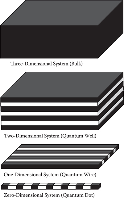
FIGURE 4.1 Three-dimensional system (bulk), two-dimensional system (quantum well), one-dimensional system (quantum wire), and zero-dimensional system (quantum dot).
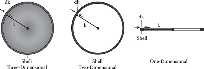
FIGURE 4.2 Shell shapes for given energy of a free electron in three-, two-, and one-dimensional systems.
Equations (4.3) and (4.4) are derived from Equation (4.2).
For the three-dimensional system, the number of states N3D contained in the shell is given by the following expression because two states with up and down spin states exist in a volume of (2π/L)3 in the k-space.
By substituting Equations (4.3) and (4.4) into Equation (4.5),
are obtained. Here, D(E) represents the density of states at energy E.
For two-dimensional systems, the number of states N2D contained in the shell is given by the following expression because two states exist in an area of (2π/L)2.
By substituting Equations (4.3) and (4.4) into Equation (4.8)
is obtained.
For one-dimensional systems, the number of states N1D contained in the shell is given by the following expression because two states exist in a length of 2π/L.
By substituting Equations (4.3) and (4.4) into Equation (4.10)
is obtained.
Figure 4.3 shows schematic diagrams of the density of states for the three-, two-, and one-dimensional systems. In three-dimensional systems, the density of states monotonically increases with energy. In two-dimensional systems, the density of states does not depend on energy. In one-dimensional systems, the density of states monotonically decreases with energy.
In Figure 4.4, dependence of electron confinement and density-of-state profiles on dimensionality is schematically summarized. In three-dimensional systems, electrons freely move in three directions, which causes the density of states to be small near the band edges and to increase with distance from the band edges. As a result, the energy gap between the conduction bands and the valence bands is diffused, giving rise to a broad absorption band. In two-dimensional systems, the translational motion freedom of electrons is reduced from three to two directions, which suppresses the increase in density of states with distance from the edges. In one-dimensional systems, the electron translational motion is allowed only in one direction, which causes the density of states to be the largest at the band edges and decrease with distance from the edges. As a result, the energy gap is defined clearly, giving rise to a sharp absorption band near the energy gap. In zero-dimensional systems, which provide a situation similar to that of atoms or small molecules, electron translational motion is not allowed, which causes the δ-function-like density-of-states profile, resulting in a sharp absorption band near the energy gap.
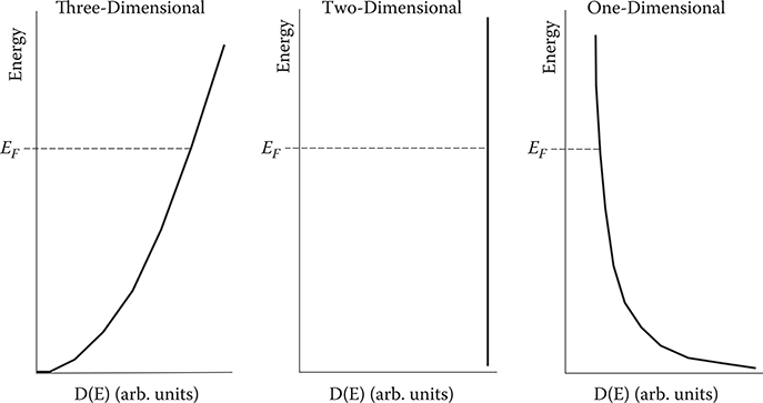
FIGURE 4.3 Schematic diagrams of the density of states for three-, two-, and one-dimensional systems.
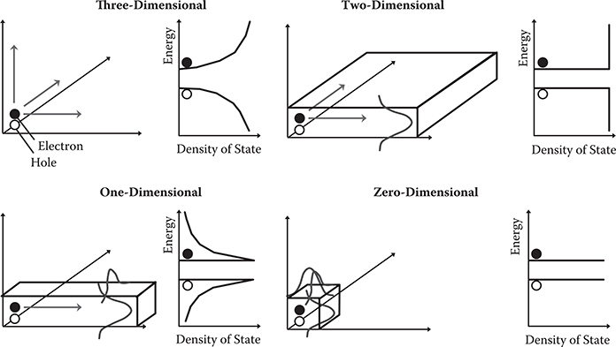
FIGURE 4.4 Dependence of electron confinement and density-of-state profiles on dimensionality.
As described in Chapter 1, quantum dots correspond to dimensionality between zero and one. The 0.5-dimensional systems correspond to long quantum dots, and the zero-dimensional systems correspond to short quantum dots. Dimensionality control between zero and one, that is, the sizes of quantum dots, can be achieved by inserting molecular units that disconnect the spread of π-electrons in conjugated polymer wires.
4.2 Quantum Dot Construction in Conjugated Polymers by MLD
4.2.1 MQD FABRICATION BY ARRANGING TWO KINDS OF MOLECULES
Molecular sequence control in polymer wires is interesting from the perspective of controlling optical and electronic properties of polymer wires to provide various kinds of photonic/electronic devices such as nonlinear optical circuits, photovoltaic devices, electroluminescent (EL) devices, biophotonic devices, molecular devices, and so on. As described in Chapter 5, it was predicted by the molecular orbital (MO) calculations that electro-optic (EO) effects in conjugated polymer wires are greatly enhanced by controlling the wavefunction shapes in the wire to optimize the wave-function separation and overlap between the excited state and the ground state [2]. For wavefunction shape optimization, dimensionality control somewhere between zero and one (i.e., quantum dot length control) is important. The dimensionality control is also effective to improve photovoltaic devices with polymer MQDs, which means polymer wires with MQD, as described in Section 9.1.
In order to realize such wavefunction control and quantum dot length control in polymer wires, molecular sequence control is essential. A promising approach to fabricate practical films of these polymers is connecting molecules one by one in order of preference. This monomolecular-step polymer wire growth process can be achieved by MLD.
For experimental demonstrations of dimensionality control between zero and one in conjugated polymer wires, we constructed quantum dots in the wires using source molecules as shown in Figure 4.5 [3]. The reaction between –CHO and –NH2 is the same as described in Section 3.3.1 for poly-AM formation. Molecules A and B are connected by double bonds through −CHO and −NH2 groups to form polymer wires. For molecule A, terephthalaldehyde (TPA) was used. For molecule B, p-phenylenediamine (PPDA), diaminodiphenyl ether (DDE), 4,4’-diaminodiphenyl sulfide (DDS), and 4,4’-diaminodiphenylmethane (DDM) were used. We fabricated quantum wire structures with long π-conjugated systems and quantum dot structures with confined π-conjugated systems in one-dimensional polymer wires. Since only two kinds of molecules, that is, molecules A and B are used in this experiment, the same polymer structures are obtained either by MLD or by vacuum deposition polymerization.
Molecules were introduced into a vacuum chamber in gas phase from temperature-controlled K cells to perform vacuum deposition polymerization. Molecular gas pressures were 1–8 × 10⁻¹ Pa, which was controlled by cell temperatures ranging from 120 to 150°C. The thickness of deposited films was measured, assuming that the film density is 1, using a quartz oscillator thickness monitor contacting the substrate holder. The substrate temperature TS was measured using a thermocouple on the holder.
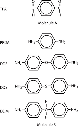
FIGURE 4.5 Source molecules for making quantum dot structures based on poly-AM. From T. Yoshimura, S. Tatsuura, W. Sotoyama, A. Matsuura, and T. Hayano, “Quantum wire and dot formation by chemical vapor deposition and molecular layer deposition of one-dimensional conjugated polymer,” Appl. Phys. Lett. 60, 268–270 (1992).
Figures 4.6(a) and (b) show the absorption spectra of poly-AM [TPA/PPDA] film grown using TPA and PPDA. The film growth rate was adjusted by cell temperatures, that is, molecular gas pressures. The growth rate increases with gas pressure. The spectra were measured at room temperature with incident light angles of 0° and 60°. Absorption bands appear in 400 to 500 nm with a sharp absorption peak of exciton observed near 500 nm, while methanol solutions of TPA and PPDA exhibit little absorption in the visible region. This indicates that long conjugated systems, that is, quantum wires, grow. The half width of the exciton absorption line for the long-wavelength side is about 50 meV. Assuming that the exciton is similar in size to that in polydiacetylene, the conjugated length is estimated to be more than the exciton length, namely, 5 nm [4]. When the film is deposited at a rate of 10 nm/min, the exciton peak is stronger for 0° than for 60°. In film deposited at 3 nm/min, the exciton peak is more dominant for 60° than for 0°. In general, exciton absorption is strong for light polarization in the wire direction. These results suggest that polymer wires stretch to the in-plane direction for 10 nm/min, while for 3 nm/min, wires tend to stretch out of the in-plane direction. Scanning electron microscope (SEM) observations with magnification of ×25,000 reveal that a beltlike texture appears on the surface of the film deposited with 10 nm/min, while no such surface structure appears for 3 nm/min. The difference in surface morphology is attributable to the wire orientation.

FIGURE 4.6 Absorption spectra of poly-AM [TPA/PPDA] film measured at room temperature with incident light angles of 0° and 60°. From T. Yoshimura, S. Tatsuura, W. Sotoyama, A. Matsuura, and T. Hayano, “Quantum wire and dot formation by chemical vapor deposition and molecular layer deposition of one-dimensional conjugated polymer,” Appl. Phys. Lett. 60, 268–270 (1992).
Note that exciton absorption becomes strong with an increased deposition rate. No exciton peak is observed for a slow deposition rate of 0.05 nm/min. We also found that the exciton absorption is enhanced by maintaining the substrate temperature to −10°C during deposition. These results indicate that, to obtain long conjugated systems, deposition conditions must be carefully optimized. It is speculated that thermal disturbance would induce a disorder in the conjugated wires.
Figure 4.7 diagrams molecules and polymer wires with their corresponding electronic potential energy curves. Benzene rings in TPA, PPDA, and DDE are regarded as a short quantum dot of ~0.5 nm in length. Poly-AM [TPA/DDE] is a polymer MQD formed by combining TPA and DDE. In the polymer MQD, the π-conjugated part is regarded as a long quantum dot with barriers of –O–. The quantum dot contains three benzene rings and the length is ~2 nm. In poly-AM [TPA/PPDA] formed by combining TPA and PPDA, π-conjugation is spread all along the wire.
Figure 4.8 shows the absorption spectra of TPA, PPDA, DDE, poly-AM [TPA/DDE], and poly-AM [TPA/PPDA]. In poly-AM [TPA/PPDA], a sharp peak of excitons is observed near 500 nm in wavelength. In poly-AM [TPA/DDE] the absorption band appears in the shorter-wavelength (higher-energy) side of that in poly-AM [TPA/PPDA] due to electron confinement in the quantum dot structure of ~2 nm in length. In TPA, PPDA, and DDE, the absorption band exhibits further higher-energy shift, indicating strong electron confinement in the short quantum dots.
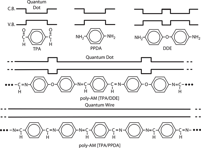
FIGURE 4.7 Molecules and polymer wires, where quantum dots and quantum wires are formed, with their corresponding electronic potential energy curves. From T. Yoshimura, S. Tatsuura, W. Sotoyama, A. Matsuura, and T. Hayano, “Quantum wire and dot formation by chemical vapor deposition and molecular layer deposition of one-dimensional conjugated polymer,” Appl. Phys. Lett. 60, 268–270 (1992).
By using DDS or DDM as molecule B, we fabricated poly-AM [TPA/DDS] and poly-AM [TPA/DDM]. In the former, –S–makes a barrier, and in the latter, –CH2–makes a barrier as –O–does in poly-AM [TPA/DDE]. Figure 4.9 shows the influence of barrier bonds on the absorption peak energy. In the order of –S–, –O–, and –CH2–, the absorption peak shifts to the higher-energy side, indicating that the barrier height increases to produce a strong electron confinement.
Energy of electrons confined in a quantum dot with infinite potential barrier height is expressed as follows in the free electron model.
Here, n = 1, 2, …, m0 is electron mass, m* is effective mass in units of m0, and L is dot length. Assuming that the effective mass is 1 and the absorption peak energy for L = ∞ equals that of poly-AM [TPA/PPDA], the excitation energy for the lowest allowed transition is calculated as a function of L as shown in Figure 4.10.

FIGURE 4.8 Absorption spectra of TPA, PPDA, DDE, poly-AM [TPA/DDE], and poly-AM [TPA/PPDA]. From T. Yoshimura, S. Tatsuura, W. Sotoyama, A. Matsuura, and T. Hayano, “Quantum wire and dot formation by chemical vapor deposition and molecular layer deposition of one-dimensional conjugated polymer,” Appl. Phys. Lett. 60, 268–270 (1992).
Experimental and calculated results agree fairly well, confirming the electron confinement in the quantum dots.
These results demonstrate the possibility of controlling dimensionality to enhance the optical nonlinearity in conjugated polymer wires and to optimize electron confinement effects for photovoltaic devices.
4.2.2 MQDS FABRICATED BY ARRANGING THREE KINDS OF MOLECULES
As described in Section 4.2.1, MQD structures can be constructed in polymer wires by arrangements of two kinds of molecules. In this case, however, the MQD structures obtained by MLD are not different from those obtained by vacuum deposition polymerization because the two molecules are automatically connected alternately even in vacuum deposition polymerization.
On the contrary, when three kinds of molecules are used for polymer wire growth, the available polymer wire structures are completely different between MLD and vacuum deposition polymerization. In the case of vacuum deposition polymerization, the three kinds of molecules are contained in the polymer wires with random sequences. In the case of MLD, on the other hand, the three kinds of molecules are contained in the polymer wires with designated arrangements. Therefore, the essential advantage of MLD appears when more than three kinds of molecules are used for polymer wire growth.

FIGURE 4.9 Influence of barrier bonds on the absorption peak energy. From T. Yoshimura, S. Tatsuura, W. Sotoyama, A. Matsuura, and T. Hayano, “Quantum wire and dot formation by chemical vapor deposition and molecular layer deposition of one-dimensional conjugated polymer,” Appl. Phys. Lett. 60, 268–270 (1992).

FIGURE 4.10 Dependence of absorption peak energy on quantum dot lengths. From T. Yoshimura, S. Tatsuura, W. Sotoyama, A. Matsuura, and T. Hayano, “Quantum wire and dot formation by chemical vapor deposition and molecular layer deposition of one-dimensional conjugated polymer,” Appl. Phys. Lett. 60, 268–270 (1992).
Considering the previously described background, we attempted to construct MQDs in polymer wires by MLD using three kinds of molecules, which is known as three-molecule MLD [5,6]. Figure 4.11 shows three kinds of molecules, that is, TPA, PPDA, and oxalic dihydrazide (ODH), and reactions between them for three-molecule MLD. TPA and PPDA are connected with a double bond, allowing the wavefunction of π-electrons to be spread over both molecules. The connection of TPA and ODH gives a series of single bonds, which cut the wavefunction at the bond. By using these bond characteristics, quantum dots can be formed in polymer wires.
Figure 4.12 shows a three-molecule MLD process for constructing polymer MQD of OTPT, where molecules are connected in a sequence of –-ODH-TPA-PPDA-TPA-ODH---. The region between two ODHs is regarded as a quantum dot since the wavefunction of π-electrons is spread through the region. The quantum dot length is around 2 nm. In Figure 4.13, structures of poly-AM quantum wire, and polymer MQDs of OTPTPT, OTPT, and OT are summarized. For OTPTPT, molecules are connected in a sequence of –-ODH-TPA-PPDA-TPA-PPDA-TPAODH---, resulting in a long quantum dot length of ~3 nm. For OT, ODH and TPA are alternately connected, resulting in a very short quantum dot length of less than 1 nm. For poly-AM, TPA and PPDA are alternately connected, so the wavefunction of π-electrons are spread through the polymer wire, creating a quantum wire.
In the present experiment, no seed cores are formed on the glass substrates. Therefore, two-sided growth MLD (shown in Figure 3.1(b)) occurs to provide symmetric growth of polymer wires. For example, in the case of OTPT, polymer wires grow by MLD as shown in Figure 4.14.
Poly-AM, OTPTPT, OTPT, and OT were experimentally fabricated by three-molecule MLD. The MLD equipment is the carrier gas type. Carrier gas of nitrogen (N2) is employed to introduce molecular gases of TPA, PPDA, and ODH in temperature-controlled molecular cells onto a glass substrate surface. MLD operation can be obtained by sequentially switching the three valves for molecular gas injection. Excess gases are removed by a rotary pump. The molecular cell temperature is 50°C for PPDA and ODH, and 25°C for TPA. The substrate surface is exposed to molecular gas for 5 min in each step. For switching molecular gases, after removing previous molecular gas by closing the valve for the gas and pumping for 5 min, the valve for the next molecular gas is opened. Switching step count is around 20. This implies that six quantum dots are contained in a polymer wire for OTPTPT, ten quantum dots for OTPT, and twenty quantum dots for OT.

FIGURE 4.11 Molecules and reactions for three-molecule MLD. From T. Yoshimura, A. Oshima, D. Kim, and Y. Morita, “Quantum dot formation in polymer wires by three-molecule molecular layer deposition (MLD) and applications to electro-optic/photovoltaic devices,” ECS Transactions 25 (4), “Atomic layer deposition applications 5,” 15–25 (2009).
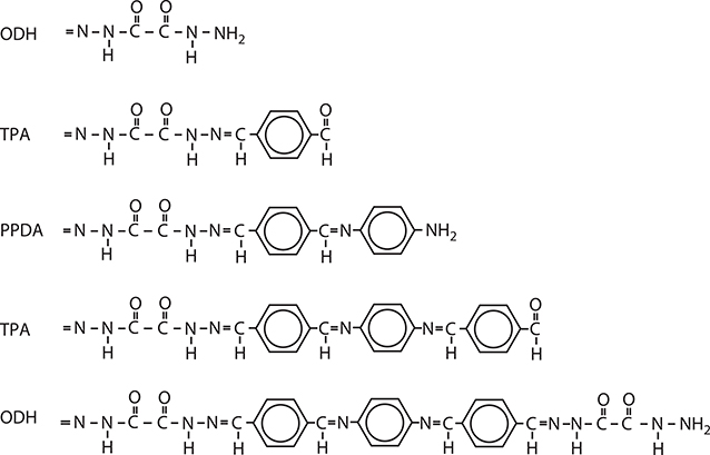
FIGURE 4.12 Three-molecule MLD process for constructing a polymer MQD of OTPT. From T. Yoshimura, A. Oshima, D. Kim, and Y. Morita, “Quantum dot formation in polymer wires by three-molecule molecular layer deposition (MLD) and applications to electro-optic/photovoltaic devices,” ECS Transactions 25 (4), “Atomic layer deposition applications 5,” 15–25 (2009).
Figure 4.15 shows absorption spectra of poly-AM quantum wire, and polymer MQDs of OTPTPT, OTPT, and OT fabricated by three-molecule MLD. In the order of poly-AM, OTPTPT, OTPT, and OT, namely, with decreasing the quantum dot lengths, the absorption peak energy shifts to the shorter-wavelength (higher-energy) side. The shift is expected to be attributed to the quantum confinement of π-electrons in quantum dots.
In order to confirm the origin for the high energy shift of the absorption peak energy, we performed calculations of absorption spectra for poly-AM, OTPTPT, OTPT, and OT by the MO method using WinMOPACK, which is the MO calculation software and is currently a part of SCIGRESS developed by Fujitsu. Figure 4.16 shows their molecular structures after structural optimization. Wirelike shapes are obtained for all the structures.
In Figure 4.17, experimental results of absorption peak energy are plotted by rectangles as a function of the quantum dot length. In the figure, absorption peak energy calculated using the MO method is also plotted by circles. Since there is a 0.3-eV offset between the calculated value and the experimental value in the absorption peak energy of the poly-AM quantum wire, the calculated absorption peak energy in Figure 4.17 is plotted by taking the experimental absorption peak energy of the poly-AM quantum wire as the standard. It is found from the figure that the experimental results and the calculated results are fairly coincident, suggesting that the absorption peak energy shift is attributed to the quantum confinement effect in MQD.

FIGURE 4.13 Structures of a poly-AM quantum wire and polymer MQDs of OTPTPT, OTPT, and OT formed by three-molecule MLD. From T. Yoshimura, A. Oshima, D. Kim, and Y. Morita, “Quantum dot formation in polymer wires by three-molecule molecular layer deposition (MLD) and applications to electro-optic/photovoltaic devices,” ECS Transactions 25 (4), “Atomic layer deposition applications 5,” 15–25 (2009).
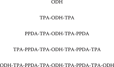
FIGURE 4.14 Three-molecule MLD for OTPT on a glass substrate without seed cores.

FIGURE 4.15 Absorption spectra of a poly-AM quantum wire, OTPTPT, OTPT, and OT. From T. Yoshimura, A. Oshima, D. Kim, and Y. Morita, “Quantum dot formation in polymer wires by three-molecule molecular layer deposition (MLD) and applications to electro-optic/photovoltaic devices,” ECS Transactions 25 (4), “Atomic layer deposition applications 5,” 15–25 (2009).
In addition, a result derived from the free-electron model in a quantum dot is presented in Figure 4.17. Energy of electrons confined in a quantum dot with infinite potential barrier height is expressed by Equation (4.12) in Section 4.2.1. Assuming that the absorption peak energy for L = ∞ equals that of the poly-AM quantum wire, the excitation energy for the lowest allowed transition is plotted. It is found that the experimental results and the calculated results based on the free-electron model agree well. This suggests that the π-electrons in the polymer wires can be regarded as free electrons in quantum dots.
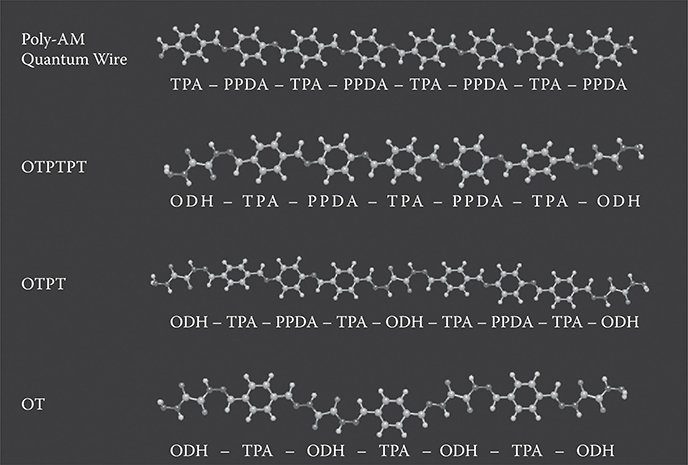
FIGURE 4.16 Molecular structures of poly-AM quantum wire, OTPTPT, OTPT, and OT after structural optimization. From T. Yoshimura, A. Oshima, D. Kim, and Y. Morita, “Quantum dot formation in polymer wires by three-molecule molecular layer deposition (MLD) and applications to electro-optic/photovoltaic devices,” ECS Transactions 25 (4), “Atomic layer deposition applications 5,” 15–25 (2009).
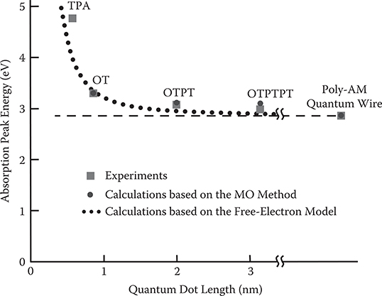
FIGURE 4.17 Dependence of absorption peak energy on quantum dot lengths. From T. Yoshimura, A. Oshima, D. Kim, and Y. Morita, “Quantum dot formation in polymer wires by three-molecule molecular layer deposition (MLD) and applications to electro-optic/photovoltaic devices,” ECS Transactions 25 (4), “Atomic layer deposition applications 5,” 15–25 (2009).
As described previously, we succeeded in controlling molecular arrangements in conjugated polymer wires with designated sequences of three kinds of molecules by three-molecule MLD and fabricating polymer MQDs. Peak energy shift of the absorption spectra of the MQDs due to the quantum confinement effect was observed. The method of controlling the arrangements of molecules of more than three kinds will enable us to control the wavefunction shapes in the polymer wires with significant freedom, providing high-performance nonlinear optical circuits, photovoltaic devices, and molecular devices. By introducing donors and acceptors into the wires, new conjugated polymer structures for use in high-performance photonic/electronic devices will be fabricated.
References
1. T. Yoshimura, Molecular nano systems: Applications to optoelectronic computers and solar energy conversion, Corona Publishing Co., Ltd., Tokyo (2007) [in Japanese].
2. T. Yoshimura, “Enhancing second-order nonlinear optical properties by controlling the wave function in one-dimensional conjugated molecules,” Phys. Rev. B40, 6292–6298 (1989).
3. T. Yoshimura, S. Tatsuura, W. Sotoyama, A. Matsuura, and T. Hayano, “Quantum wire and dot formation by chemical vapor deposition and molecular layer deposition of one-dimensional conjugated polymer,” Appl. Phys. Lett. 60, 268–270 (1992).
4. B. I. Greene, J. Orenstein, R. R. Millard, and L. R. Williams, “Nonlinear optical response of excitons confined to one dimension,” Phys. Rev. Lett. 58, 2750–2753 (1987).
5. A. Oshima and T. Yoshimura, “Controlling sequences of three molecules and quantum dot lengths in conjugated polymer wires by molecular layer deposition,” AVS, 9th International Conference on Atomic Layer Deposition, Monterey, California, 149 (2009).
6. T. Yoshimura, A. Oshima, D. Kim, and Y. Morita, “Quantum dot formation in polymer wires by three-molecule molecular layer deposition (MLD) and applications to electro-optic/photovoltaic devices,” ECS Transactions 25 (4) “Atomic layer deposition applications 5,” from the 216th ECS Meeting, Vienna, Austria, 15–25 (2009).