
6 Design of Integrated Optical Switches
High-speed, thin and small light modulators and optical switches are the key devices in optical interconnects and optical switching systems; they improve the computer processing speed and the communication capacity. The polymer multiple quantum dot (MQD) fabricated by molecular layer deposition (MLD) is a promising future material for integrated light modulators and optical switches.
Mach-Zehnder interferometer and directional coupler type light modulators and optical switches utilizing the electro-optic (EO) effect are well known. However, these devices are largely affected by temperature and processing accuracy for device fabrication since they are phase-sensitive devices; consequently, their large-scale integration is difficult.
In Figure 6.1, structures of promising light modulator and optical switch candidates are shown, such as the variable well optical IC (VWOIC) [1, 2, 3 and 4], the waveguide prism deflector (WPD) optical switch [2, 3, 4, 5, 6, 7, 8, 9 and 10], the total internal reflection (TIR) optical switch, the digital optical switch, the ring resonator optical switch, and the photonic crystal. The VWOIC, WPD optical switch, TIR optical switch, and digital optical switch are phase-insensitive flux-controlled devices that are suitable for large-scale integration.
Examples of EO material candidates for light modulators and optical switches are listed in Table 6.1. Materials having the Pockels effect are LiNbO3 (LN), III–V semiconductor quantum dot (QD) [11,12], styrylpyridinium cyanine dye (SPCD) [13], which is a molecular crystal, and polymer MQD [14, 15 and 16], which is an artificial material consisting of polymer wires with MQDs. The EO property of polymer MQDs is theoretically predicted in Chapter 5 [16]. EO material having the Kerr effect is lead lanthanum zirconate titanate (PLZT) [17]. The polymer MQD might also be expected to exhibit a large Kerr effect, although precise analysis was not done. Electric-field-induced refractive index change, Δn, is calculated by the following expressions.
Here, n and E represent the refractive index of the EO material and electric field in the materials. r and R are, respectively, the EO coefficients for the Pockels effect and the Kerr effect. Figure 6.2 shows the expected Δn that is induced when 1 V is applied between electrodes on the top and bottom surfaces of 1-µm-thick EO materials. It is found that III-V semiconductor QD and SPCD exhibit large Δn as compared with lithium niobate (LN). PLZT and polymer MQD exhibit extremely large Δn. Δn of more than 0.01 is theoretically expected with a few volts applied.
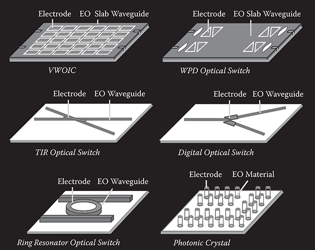
FIGURE 6.1 Structures of light modulators and optical switches.
TABLE 6.1
Typical Properties of EO Material Candidates for Light Modulators and Optical Switches

In this chapter, the design and predicted performance of VWOICs and WPD optical switches previously proposed by the author are reviewed. The VWOIC and the WPD optical switch are especially superior as EO switches for integrated polymer optical circuits with a large number of elements. Ring resonator optical switches that are expected as ultrasmall optical switches are briefly described. In addition, bandwidth limit in photonic crystal waveguides is discussed.
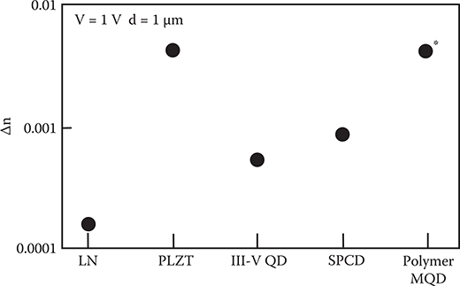
FIGURE 6.2 Expected electric-field-induced refractive index change Δn for typical EO materials. The solid circle with an asterisk (*) is the theoretically predicted value diselectrode seperation.
Since light modulators and optical switches have the same structures in many cases, light modulators are discussed along with optical switches in the following text.
6.1 Variable well Optical Ics (VWOICS) and Waveguide Prism Deflectors (WPDS)
Structures of the VWOIC [1–4] and the WPD optical switch [2–10] are schematically shown in Figure 6.3. In the former, rectangular electrodes are formed on an EO slab waveguide. In the latter, prism-shaped cascading electrodes are formed on an EO slab waveguide. The slab waveguides consist of three layers (clad/core/clad) placed between counter electrodes and rectangular or prism-shaped electrodes. The clad is not drawn in the figure. The core is made of EO materials and the refractive index changes by electric fields. Interface films, in which thin-film interface ICs are embedded, are stacked on the surface for driving the individual optical switches to perform selective voltage application to the electrodes.
As Figure 6.4 shows, in VWOIC, by selectively applying voltage to the EO waveguide through the patterned electrodes, refractive index change is induced to form potential wells for light waves (see Section 2.1). Then, electric-field-induced dynamic optical waveguides are constructed all over the slab waveguide to switch guided light beams. In WPD optical switches, as shown in Figure 6.5, electric-field-induced dynamic prisms, which deflect guided light beams introduced from input waveguides, are constructed, enabling us to switch the light beams through two-dimensional (2-D) free space region in the slab waveguide like “search lights.” Waveguide lenses for light beam collimation are formed to suppress spreading due to diffraction of the propagating light beams in the free space region.

FIGURE 6.3 Structures of the VWOIC and the WPD optical switch.
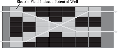
FIGURE 6.4 Operation principle of the VWOIC. From T. Yoshimura, S. Tsukada, S. Kawakami, Y. Arai, H. Kurokawa, and K. Asama, “3D micro optical switching system (3D-MOSS) architecture,” Proc. SPIE 4653, 62–70 (2002).
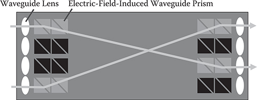
FIGURE 6.5 Operation principle of the WPD optical switch. From T. Yoshimura, S. Tsukada, S. Kawakami, Y. Arai, H. Kurokawa, and K. Asama, “3D micro optical switching system (3D-MOSS) architecture,” Proc. SPIE 4653, 62–70 (2002).
Optical switches for optical interconnects within computers and optical switching systems should be high speed, thin, small, and at the same time, should be stable when subjected to the considerable thermal and device shape/configuration disturbance that is present. In ordinary optical switches, such as Mach-Zehnder switches and directional coupler switches, a small phase difference is used for the switching operation. Therefore, the dependence of the device operation on temperature and processing accuracy in device fabrication is large. In fact, in a LiNbO3 matrix optical switch, individual precise adjustment of driving voltage is required for each element in the 8 × 8 scale.
On the contrary, VWOICs and WPD optical switches are phase-insensitive flux-controlled devices. That is, electric-field-induced refractive index differences in the slab waveguide are used to switch the optical path directly. The refractive index difference is relatively insensitive to the temperature changes compared with the refractive index itself. Furthermore, for processing accuracy, as far as the edge angles of electrodes are concerned, the size of each part does not largely affect the switching characteristics. Therefore, VWOICs and WPD optical switches are expected to exhibit stable operation compared with ordinary optical switches, and to be suitable for large-scale optical systems such as integrated optical interconnects within boxes and three-dimensional micro-optical switching systems (3D-MOSSs) described in Chapter 8.
6.1.1 DESIGN OF VWOIC
The switching operation was simulated by the beam propagation method (BPM) for VWOIC with 12 × 7 electrodes of 2 µm × 100 µm. The results are shown in Figure 6.6 for a wavelength of 1.3 µm. The refractive index change induced by voltage application is assumed to be 0.005. Two adjacent electrodes are simultaneously selected for voltage application, which corresponds to 4-µm-wide waveguide construction. Selected regions are shifted by 2 µm along a direction perpendicular to the light propagation direction in order to achieve quasicontinuous index variation. It can be seen that a light beam is switched in a length of 700 µm.
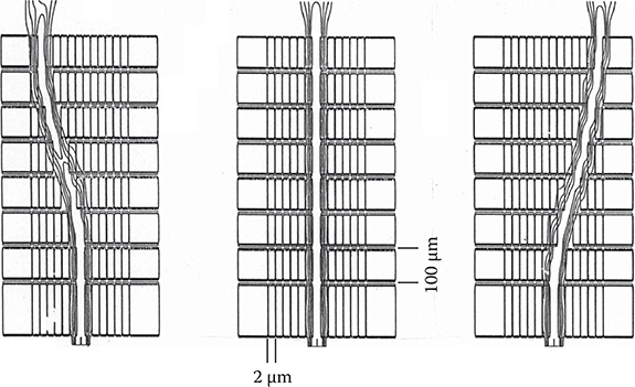
FIGURE 6.6 Switching operation of VWOIC simulated by the BPM. From T. Yoshimura, S. Tsukada, S. Kawakami, Y. Arai, H. Kurokawa, and K. Asama, “3D micro optical switching system (3D-MOSS) architecture,” Proc. SPIE 4653, 62–70 (2002).
6.1.2 DESIGN OF WPD OPTICAL SWITCH UTILIZING THE POCKELS EFFECT
6.1.2.1 Simulation procedure
When designing the WPD optical switches, the following two are the objectives.
Reduction of the prism size and the interchannel pitch
Suppression of the beam spreading accompanying the free space propagation in the slab waveguide
These two objectives have a reciprocal relationship. If the prism size is reduced, the prism aperture decreases and the diffraction angle increases. Consequently, the beam spreading increases. So it is important to find a practical solution for the WPD optical switch structure within this trade-off.
As shown in Figure 6.7, the prism electrode is formed by a pair. When a −V voltage is applied to one electrode and a +V voltage to the other, prism-shaped refractive index changes of −Δn and +Δn are induced in the slab waveguide under the electrodes. As a result, a waveguide prism is produced, and the light beams are deflected. The deflection angle θd is given by the following equation from the incident angle θ1 and the transmission angle θ2.
By lining up multiple prism electrode pairs in a cascade, a larger deflection angle can be obtained. The polarity of the voltage pattern of the prism-shaped electrodes at the output is reversed. Thus, the deflected light beams return in the horizontal direction and can smoothly couple to the output waveguide. The light beams introduced from the input waveguide spread as they propagate in the slab waveguide.
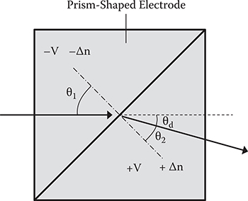
FIGURE 6.7 Detail of the electric-field-induced waveguide prism in a slab waveguide with the Pockels effect. From M. Ninomiya, Y. Arai, T. Yoshimura, H. Kurokawa, and K. Asama, “Characteristics evaluation for waveguide-prism-deflector type micro optical switches (WPD-MOS),” Electronics and Communications in Japan, Part 2 86, 38–48 (2003).
The switching characteristics are simulated by the 2-D analysis of wide-angle approximate BPM using the finite difference method. The propagating light beam has a wavelength λ of 1.3 µm and is in transverse electric (TE) mode. The Δz step in the light beam propagation direction is set to 0.5 µm and the Δx step in the perpendicular direction is set to λ/30. The core refractive index of the input and output waveguides is equal to the core refractive index of the slab waveguide, that is, the refractive index of the EO material with no applied voltage. The difference in the refractive index between the core and the clad is set to 0.03. The electric field distribution of the input light beam is that of the input waveguide fundamental mode. The integrated intensity of the input light beam is 1.0.
For the present simulation, EO material is assumed to be a 400-nm-thick SPCD film with r = 430 pm/V and n = 1.55. When 6.6 V is applied to the 400-nm-thick EO waveguide, a refractive index change of about Δn = 0.013 is theoretically expected.
6.1.2.2 Structural Model
Figure 6.8 is a top view of a WPD optical switch model with a SPCD slab waveguide. The pitch of the input and output waveguides with an aperture of D is set to P µm, and the number of steps of the prism electrode pair to N. The prism electrode has a right-angle triangle shape with a length and an aperture of DP.
The distance Ld between the prisms required for switching is estimated. For convenience, Ld is defined as the distance to the center of the multistage prisms at the input and the output. The refractive index n1 in the negative voltage application unit and the refractive index n2 of the positive voltage application unit are expressed as follows using the electric-field-induced refractive index change Δn:
where n0 is the refractive index when no voltage is applied. From the refraction rule at the prism electrode boundary, the relationship between the incident angle θ1 and the transmission angle θ2 is given by
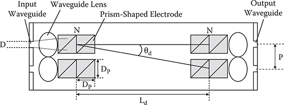
FIGURE 6.8 Top view of WPD optical switch model with SPCD slab waveguide. From M. Ninomiya, Y. Arai, T. Yoshimura, H. Kurokawa, and K. Asama, “Characteristics evaluation for waveguide-prism-deflector type micro optical switches (WPD-MOS),” Electronics and Communications in Japan, Part 2 86, 38–48 (2003).
The deflection angle θd is determined from Equations (6.6) and (6.3). For an N-stage cascade, N iterations of the calculation in Equation (6.6) determines the final θd. Ld in the zeroth approximation is expressed in terms of θd and P by the following:
The diffraction angle of the light beams increases with decreasing D. The beam diameter must be less than or equal to the waveguide pitch P. Therefore, restrictions develop in Ld depending on D.
6.1.2.3 Simulated Performance
6.1.2.3.1 2 × 2 WPD Optical Switch
From preliminary tests, N = 4 and V = 11 V was extracted as the appropriate condition for WPD optical switches with SPCD. A 2 × 2 WPD optical switch structure is created with this condition as shown in Figure 6.9. Here, P = 20 µm, D = 4 µm, and DP = 16 µm. The diameter and the refractive index of the lens are 40 µm and 2.0, respectively. The optical switching length is 390 µm.
Figure 6.10 shows the Input 1 −> Output 1 switching and Input 2 −> Output 1 switching simulated by the BPM. Light beam deflection by the waveguide prism and smooth switching operation are observed. For Input 1 −> Output 1, the crosstalk was −12 dB and the insertion loss, 0.44 dB. For Input 2 −> Output 1, the crosstalk was −14 dB and the insertion loss, 0.96 dB. Thus, the overall WPD optical switch characteristics were the crosstalk ≤ –12dB, the insertion loss ≤0.96dB.
6.1.2.3.2 3 × 3 WPD Optical Switch
Figure 6.11 shows a 3 × 3 WPD optical switch structure. Figure 6.12 shows the voltage application patterns, and Figure 6.13 shows the switching operation simulated by the BPM for Input 1 −> Output 3 and Input 1 −> Output 2. The crosstalk was ≤−10 dB, insertion loss was ≤1.2 dB, and the length was 400 µm. Thus, the possibility of a 3 × 3 optical switch with a length of less than 1 mm was demonstrated.
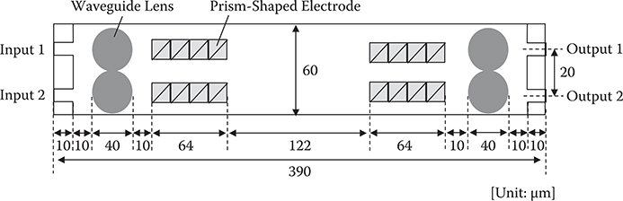
FIGURE 6.9 Typical structure of 2 × 2 WPD optical switch with SPCD slab waveguide. From M. Ninomiya, Y. Arai, T. Yoshimura, H. Kurokawa, and K. Asama, “Characteristics evaluation for waveguide-prism-deflector type micro optical switches (WPD-MOS),” Electronics and Communications in Japan, Part 2 86, 38–48 (2003).
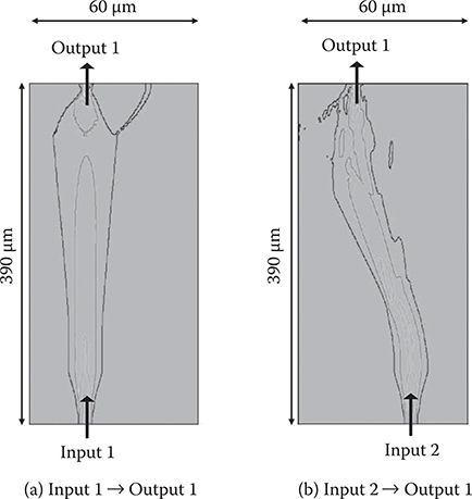
FIGURE 6.10 Switching operation of 2 × 2 WPD optical switch with SPCD slab waveguide simulated by the BPM. From M. Ninomiya, Y. Arai, T. Yoshimura, H. Kurokawa, and K. Asama, “Characteristics evaluation for waveguide-prism-deflector type micro optical switches (WPD-MOS),” Electronics and Communications in Japan, Part 2 86, 38–48 (2003).
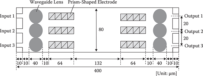
FIGURE 6.11 Structure of 3 × 3 WPD optical switch with SPCD slab waveguide. From M. Ninomiya, Y. Arai, T. Yoshimura, H. Kurokawa, and K. Asama, “Characteristics evaluation for waveguide-prism-deflector type micro optical switches (WPD-MOS),” Electronics and Communications in Japan, Part 2 86, 38–48 (2003).
6.1.2.3.3 Switching Time
The switching time τ of a WPD optical switch is given by the following equation,
where the ON resistance of the drive circuit is RON [Ω] and the capacitance between the prism electrode and the counter electrode is C [F].
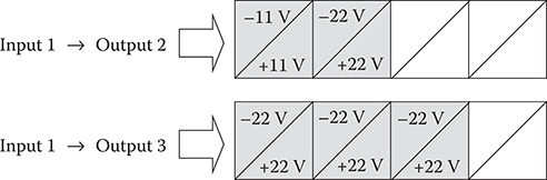
FIGURE 6.12 Voltage application patterns to prism-shaped electrodes in 3 × 3 WPD optical switch. From M. Ninomiya, Y. Arai, T. Yoshimura, H. Kurokawa, and K. Asama, “Characteristics evaluation for waveguide-prism-deflector type micro optical switches (WPD-MOS),” Electronics and Communications in Japan, Part 2 86, 38–48 (2003).
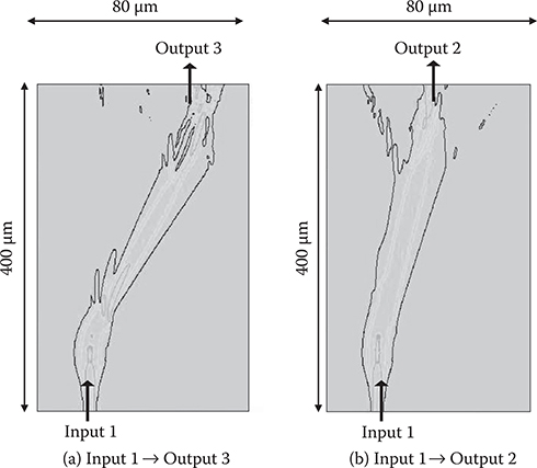
FIGURE 6.13 Switching operation of 3 × 3 WPD optical switch with SPCD slab waveguide simulated by the BPM. From M. Ninomiya, Y. Arai, T. Yoshimura, H. Kurokawa, and K. Asama, “Characteristics evaluation for waveguide-prism-deflector type micro optical switches (WPD-MOS),” Electronics and Communications in Japan, Part 2 86, 38–48 (2003).
When the area of the prism-shaped electrode is S [m2], the distance between electrodes is d [m], and the dielectric constant of the EO material is ε, C is given by
By substituting S = (1/2) × (16 × 10−6) × (16 × 10−6) = 128 × 10−12 m2, d = 4 × 10⁻⁷ m, and the assumed dielectric constant of SPCD, ε ≈ 4 ε0, into Equation (6.9), C = 11 fF is obtained. Then, from Equation (6.8), τ is calculated to be 1.1 ps for RON = 100 Ω. We see that the speed of the switch is sufficiently fast.
Power consumption Power is given by
where F is switching rate. When F = 5 × 10⁹ 1/s and V = 11 V, power consumption is calculated to be 6.9 mW.
6.1.3 DESIGN OF WPD OPTICAL SWITCH UTILIZING the KERR EFFECT
As Figure 6.2 shows, PLZT is expected to exhibit a large electric-field-induced refractive index change due to its large Kerr coefficient. In the present subsection, design, simulated switching operation, and a preliminary experimental result of WPD optical switches utilizing PLZT thin films are reviewed.
6.1.3.1 Simulation procedure
A top view of a WPD optical switch model with PLZT slab waveguide is shown in Figure 6.14. The same voltage is applied to the input-side electrodes and output-side electrodes in order to make the deflected light path parallel to the output waveguides.
Light wavelength λ is assumed to be 1.3 µm. Input and output waveguides consist of a channel waveguide with a core width D of 4 µm, a core refractive index nCore of 1.52, and a clad refractive index nClad of 1.50, which permits the propagation of the fundamental mode with m = 0 and the first excited mode with m = 1. Channel distance P is 20 µm. Waveguide lens diameter DLens is 40 µm. The lens expands the light beam size to DB. Right-angle prism-shaped electrodes with an aperture DP of 16 µm and length 2DP are formed on the slab waveguide with a separation d of 400 nm from a counter electrode beneath the PLZT film. Two-step prism cascading configuration is considered.
Reflections from the integrated components such as waveguide lenses were not taken into account. Anti-reflective (AR) coating on the component edge surfaces using atomic layer deposition (ALD) or MLD, which can grow ultrathin conformal films on surfaces with three-dimensional structures such as trenches, might make the model viable.
6.1.3.2 Structural Model
In order to determine a rough sketch of WPD optical switch structure, an estimation for EO slab waveguide length LEO is carried out. A detail of the electric-field-induced waveguide prism is shown in Figure 6.15. The refractive index change Δn is induced in the EO slab waveguide by a driving voltage V according to Equation (6.2). Waveguide prism refractive index nP is given by
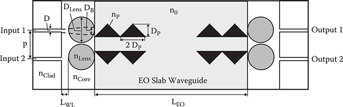
FIGURE 6.14 Top view of WPD optical switch model with PLZT slab waveguide.
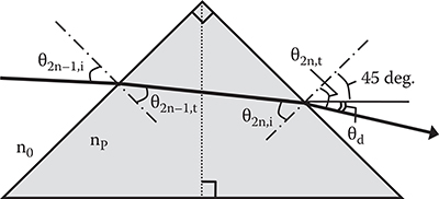
FIGURE 6.15 Detail of the electric-field-induced waveguide prism in a slab waveguide with the Kerr effect. From T. Yoshimura, M. Ojima, Y. Arai, N. Fujimoto, and K. Asama, “Simulation on cross-talk reduction in multi-mode-waveguide-based micro optical switching systems using single mode filters,” Appl. Opt. 43, 1390–1395 (2003).
Here, n0 is the refractive index of the EO slab waveguide with no applied voltage. Deflection angle θd can be calculated using the following equations:
As the 0th approximation, neglecting the size of prism-shaped electrodes, LEO is given by
The Diffraction angle of light beams propagating in the slab waveguide is expressed as θ = λ/(πn0DB). The light beam width should be less than P at the end of the EO slab waveguide after propagation. Then, LEO should satisfy
In Figure 6.16, V dependence of LEO derived from Equations (6.2) and (6.11) through (6.13) using the parameters for PLZT shown in Table 6.1 is shown for a two-step prism cascading configuration (N = 2). The diffraction limit boundary obtained by Equation (6.14) is also shown for DB of 5 µm. It can be seen that the lowest possible driving voltage is around 1 V, predicting LEO of several hundred µm. In the present simulation, V = 1.2 V is assumed, which generates a waveguide prism refractive index nP(On) of 2.52 derived from Equations (6.2) and (6.11). The waveguide prism refractive index nP(Off) for 0 − V application is equal to n0 of 2.48.
Based on the parameters mentioned above, the waveguide lens refractive index nLens, the distance between the waveguide lens and the input/output waveguide LWL, and LEO are optimized. Figure 6.17 shows beam propagation in the slab waveguide simulated by BPM for nLens of 1.8, 2.0, and 2.5. For nLens = 1.8, collimation of the light beam in the EO slab waveguide is insufficient, while for nLens of 2.5 the focusing effect is too strong, and large beam size expansion occurs. nLens of 2.0 is a proper condition to produce collimated light beams, resulting in smooth coupling to the output waveguide at a distance of 310 µm from the input waveguide. Figure 6.18(a) shows LWL dependence of transmission efficiency from the input waveguide into the output waveguide. The optimum LWL is found to be 20 µm. For LEO, as shown in Figure 6.18(b), the optimum is 190–200 µm. From a viewpoint of miniaturization of optical switches, 190 µm should be the optimum LEO. Thus, the total length of the WPD optical switch is calculated to be 310 µm by adding 2(DLens + LWL) to LEO.
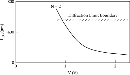
FIGURE 6.16 V dependence of LEO and diffraction limit for LEO. From T. Yoshimura, M. Ojima, Y. Arai, N. Fujimoto, and K. Asama, “Simulation on cross-talk reduction in multimode-waveguide-based micro optical switching systems using single mode filters,” Appl. Opt. 43, 1390–1395 (2003).
Design parameters determined for the WPD optical switch are summarized in Table 6.2 and the typical structure of a WPD optical switch is shown in Figure 6.19. The slab waveguide is divided into two regions. One is a region with waveguide lenses. The waveguide lens refractive index of 2.00 is available by using TixSiyO, for example. The other is a region with prisms where the entire slab waveguide is made of 400-nm-thick PLZT. Right-angle prism-shaped electrodes with an area of 16 × 16 µm2 are formed on the slab waveguide. The size of the main switch part is 310 µm × 20 µm. When channel separation is widened to 60 µm by bending waveguides of 2.5-mm radius at the input and output ports, the total switch length LSW and width WSW become 1190 µm and 100 µm, respectively.
6.1.3.3 Simulated Performance
Figure 6.20 shows the switching operation of the WPD optical switch simulated by the BPM. When no voltages are applied to the prism-shaped electrodes, a light beam propagates from Input 1 to Output 1, achieving a bar condition. By 1.2-V application to the electrodes, a light beam propagates from Input 1 to Output 2, achieving a cross condition. For both the bar and cross conditions, cross-talk is less than −20 dB. Transmission efficiency is 80% and 69% for bar and cross, respectively. The maximum insertion loss within the WPD optical switch is 1.7 dB including losses in bending waveguides.
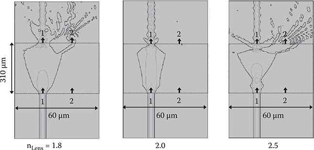
FIGURE 6.17 Beam propagation in the slab waveguide with waveguide lenses simulated by the BPM. From T. Yoshimura, M. Ojima, Y. Arai, N. Fujimoto, and K. Asama, “Simulation on cross-talk reduction in multi-mode-waveguide-based micro optical switching systems using single mode filters,” Appl. Opt. 43, 1390–1395 (2003).

FIGURE 6.18 Dependence of transmission efficiency into the output waveguide on (a) LWL and (b) LEO. From T. Yoshimura, M. Ojima, Y. Arai, N. Fujimoto, and K. Asama, “Simulation on cross-talk reduction in multi-mode-waveguide-based micro optical switching systems using single mode filters,” Appl. Opt. 43, 1390–1395 (2003).
TABLE 6.2
Design Parameters for the WPD Optical Switch
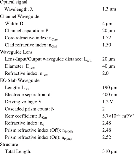
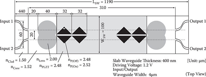
FIGURE 6.19 Typical structure of WPD optical switch with PLZT slab waveguide. From T. Yoshimura, M. Ojima, Y. Arai, and K. Asama, “Three-dimensional self-organized micro optoelectronic systems for board-level reconfigurable optical interconnects: Performance modeling and simulation,” IEEE J. Select. Topics in Quantum Electron. 9, 492–511 (2003).
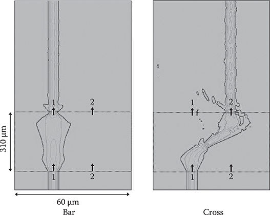
FIGURE 6.20 Switching operation of WPD optical switch with PLZT slab waveguide simulated by the BPM. From T. Yoshimura, M. Ojima, Y. Arai, N. Fujimoto, and K. Asama, “Simulation on cross-talk reduction in multi-mode-waveguide-based micro optical switching systems using single mode filters,” Appl. Opt. 43, 1390–1395 (2003).
Switching speed and power consumption can be estimated based on a charge–discharge model for a prism-shaped capacitor as the 0th approximation. A waveguide prism deflector is regarded as a capacitor with an area of S, a thickness of d, and a dielectric constant of ε. The capacitance C, switching speed τ, and power consumption Power are respectively given by Equations (6.9), (6.8), and (6.10). In the model shown in Figure 6.19, S = 256 × 10−12 m2, d = 4 × 10⁻⁷ m, and the dielectric constant of PLZT ε = 1000ε0. Then, C, τ, and Power are respectively calculated to be 5.7 pF, 570 ps for RON = 100 Ω, and 41 mW for F = 5 × 10⁹ 1/s and V = 1.2 V.
6.1.4 IMPACT OF POLYMER MQDS ON OPTICAL SWITCH PERFORMANCE
As Table 6.1 and Figure 6.2 show, the polymer MQD [14–16] is theoretically expected to exhibit large EO effects and a low dielectric constant, say, around 4ε0, which will improve switching performance of optical switches. Figure 6.21 shows EO material dependence of switching operation of WPD optical switches simulated by the BPM. When the DAAD-type polymer MQD described in Chapter 5 is used, large deflection angles induced by small driving voltages are expected.
The dielectric constant for electrical signals is expected to be much smaller in the polymer MQD than in PLZT because the EO effect in the polymer wires mainly arises from electronic polarization while that in PLZT arises from atomic polarization. This feature of the polymer MQD is desirable to achieve high-speed and low power operations. When ε for the polymer MQD is 4ε0 and PLZT 1000ε0, τ and Power for the polymer MQD can be 1/250 of those for PLZT. Thus, the polymer MQD is expected to remove the drawbacks of slow switching time and large power consumption in PLZT. The polymer MQD is an ideal EO material for large-scale integrated optical interconnects and optical switching systems.

FIGURE 6.21 Improvement of WPD optical switches by utilizing the polymer MQD simulated by the BPM.
6.1.5 FUTURE INTEGRATION ISSUES
The present simulation indicates the possibility of 2 × 2 and 3 × 3 WPD optical switches having lengths of 100-µm scales. However, the method for connecting and integrating the driver circuits, optical waveguide systems, and optical switches is a serious problem when building actual systems. The connecting and the integrating will be achieved by using PL-Pack with SORT (described in Section 7.5), which transplants different thin-film devices and materials together into a substrate. EO thin films of the optical switches may be easily integrated with optical waveguides, waveguide lenses, waveguide filters, and waveguide mirrors by PL-PACK with SORT. For integration of EO thin films made of the polymer MQDs, molecular nano duplication (MND) (described in Section 3.7) may be applicable. SOLNET, which is described in Section 7.4, is useful to connect the EO thin films to optical waveguides and other optical devices even when misalignment exists between them.
6.1.6 EXPERIMENTAL DEMONSTRATION OF WPD UTILIZING PLZT
As a preliminary demonstration, we fabricated a WPD using a PLZT slab waveguide using the process shown at the top in Figure 6.22. A patterned indium tin oxide (ITO) transparent electrode was formed on a glass substrate. Then, a thin film of PLZT was applied on it by sol-gel method. The PLZT film thickness was 250 nm. On the film surface an Al counter electrode was deposited by vacuum evaporation. Figure 6.22 shows guided beam deflection by applying 35 V between the ITO and Al electrodes. A deflection angle of 1.1o was observed.
The future challenges are optimization of the PLZT WPD optical switches and replacement of PLZT with the polymer MQD.
6.2 Nano-Scale Optical Switches
6.2.1 RING RESONATOR OPTICAL SWITCHES
For ultrasmall optical switches, although the thermal stability is usually insufficient, ring resonators consisting of high-index contrast (HIC) waveguides might be a possible candidate. In the present section, light beam propagation and switching operation in the ring resonator optical switch are simulated by the finite difference time domain (FDTD) method.
Ring resonator optical switches have been developed by many researchers. A typical model is shown in Figure 6.23. Between two straight waveguides, a ring EO waveguide is inserted. The core width of these optical waveguides is usually submicrons. Figure 6.24 shows propagation of a light pulse in a ring resonator optical switch consisting of PLZT. The light polarization is parallel to the z-axis. A light pulse introduced from Input 1 is partially transferred between the straight waveguides and the ring EO waveguide.
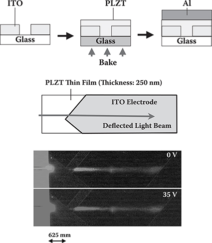
FIGURE 6.22 Light beam deflection in a WPD light modulator using a PLZT slab waveguide.
When the device configuration and the refractive index of the optical waveguides are appropriately tuned in a resonance condition, continuous wave (CW) light beam gradually becomes localized into the ring EO waveguide, as can be seen in Figure 6.25. At the same time, the light beam that was guided to Output 2 is switched to Output 1. When a voltage is applied to the ring EO waveguide, the resonance condition is broken to switch the light beam from Output 2 to Output 1, as shown in Figure 6.26.

FIGURE 6.23 Model of a ring resonator optical switch.
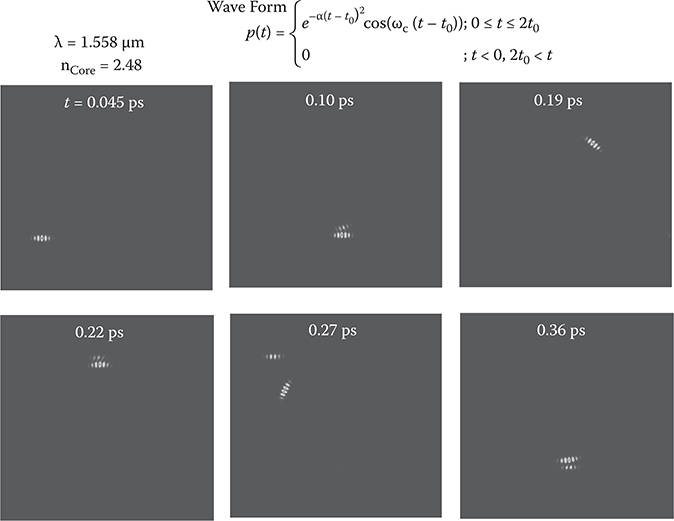
FIGURE 6.24 Propagation of a light pulse in a ring resonator optical switch simulated by the FDTD method. The brightness is automatically adjusted.
The resonance condition varies with the wavelength of the guided beam. Therefore, the ring resonator optical switch acts as a wavelength filter, too. By applying a voltage to the ring EO waveguide, the resonance wavelength is controlled, enabling tunable wavelength filter operation.
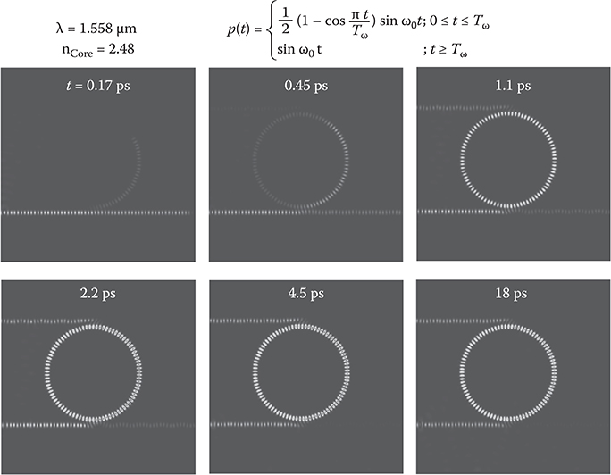
FIGURE 6.25 Resonance of light waves in a ring resonator optical switch simulated by the FDTD method.
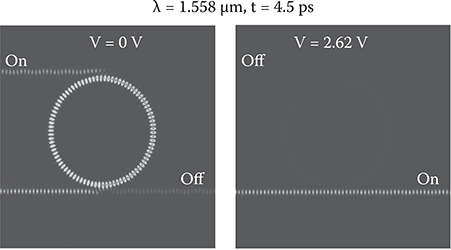
FIGURE 6.26 Switching operation of a ring resonator optical switch simulated by the FDTD method.
6.2.2 BANDWIDTH LIMIT IN PHOTONIC CRYSTAL WAVEGUIDES
The photonic crystal, which was proposed and developed by Yablonovitch [18], has periodic variations of the refractive index like dielectric multilayer wavelength filters. As the energy bands and energy gap for electrons in crystals that have periodic potential variations, the energy bands and photonic band gap (PBG) for photons appear in photonic crystals as shown in Figure 6.27. When the energy of photons is in the PBG region, light beams cannot exist in the photonic crystals in steady states. When the energy of photons is out of the PBG region, light beams can exist in the photonic crystals.
If some imperfections are created in a photonic crystal, light beams with photon energy within the PBG can exist in the imperfect parts. By creating line-shaped imperfections as shown in Figure 6.27, light beams are confined in the imperfect parts because they cannot exist in the surrounding perfect photonic crystal parts. The line width of the imperfection can be submicrons. Thus, nano-scale waveguides can be constructed in the photonic crystal. By implementation of EO materials into the photonic crystal, ultrasmall optical switches might be available.
Simulation for light beam propagation in a 2-D photonic crystal waveguide was carried out using the FDTD method. The results are shown in Figures 6.28 and 6.29. Holes with a 104-nm radius are arranged with a 521-nm pitch in a medium with a refractive index of 3.38. Light polarization is parallel to the z-axis. For wavelength λ = 1.19 µm, which corresponds to photon energy out of the PBG, light beams are leaked from the optical waveguide. For wavelength λ = 1.30 µm, which corresponds to photon energy near the center of the PBG, light beams are strongly confined in the optical waveguide.
Here, however, it should be noted that at the initial stage of light incidence, that is, at time duration (t) of 0.11 ps, confined light intensity is weak, and with time it gradually increases to reach a saturated state. Figure 6.30 shows a result for transient light beam propagation in the photonic crystal waveguide [19]. The drawing contrast is adjusted to enhance leaked light beams in the surrounding perfect crystal region. It is found that at the initial stage, considerable leakage of light beams into the surrounding perfect crystal region is observed. After 0.6 ps, the leakage is suppressed and strong confinement of light beams in the optical waveguide is accomplished.
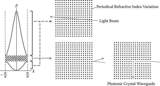
FIGURE 6.27 Band diagrams for a photonic crystal and light beam propagation in it.

FIGURE 6.28 Light beam propagation in a photonic crystal waveguide for a wavelength out of the PBG simulated by the FDTD method.
A delay before settling waveguide functions arises from the fact that the photonic crystal device uses interference of light beams at a steady state. In the model shown in Figure 6.30, at t = 0.05 and 0.1 ps, only a part of reflected light beams are in the photonic crystal, that is, light beam interference in the photonic crystal is not completed yet. At t = 0.6 ps, since 0.6 ps corresponds to a light beam propagation distance of ~150 µm that is 17 times the photonic crystal size in the present model, the interference is built up completely, that is, superposition of all the reflected light beams is completed in the entire photonic crystal, to reach the steady state. Thus, the leakage is suppressed, resulting in perfect light beam confinement in the optical waveguide.
Transient responses of light beam confinement in a photonic crystal waveguide are shown in Figure 6.31. For wavelength λ = 1.20 µm, which corresponds to photon energy at the edge of the PBG, a long delay of ~0.5 ps is observed before the confined light intensity reaches its steady state. For wavelength λ = 1.30 µm located near the rods of the polymer MQD. By applying voltages to the rods, some optical switching operation might occur. For the ring resonator optical switches, the same process is applicable by forming seed cores with ring waveguide patterns.

FIGURE 6.29 Light beam propagation in a photonic crystal waveguide for a wavelength within the PBG simulated by the FDTD method.
6.2.3 Polymer MQDs in Nano-Scale Optical Switches
As mentioned in Section 6.1.4, the polymer MQD fabricated by MLD is expected to be a promising EO material. It will be a great challenge to realize high-performance optical switches with ring resonator and photonic crystal structures consisting of the polymer MQD.
Figure 6.33 shows a concept of a photonic crystal optical switch with the polymer MQD fabricated by MLD using seed cores, as described in Section 3.4. First, seed cores with a pattern of a photonic crystal waveguide are formed on a substrate surface. Then, by MLD, polymer wires are grown from the seed cores to form EO rods of the polymer MQD. By applying voltages to the rods, some optical switching operation might occur. For the ring resonator optical switches, the same process is applicable by forming seed cores with ring waveguide patterns.
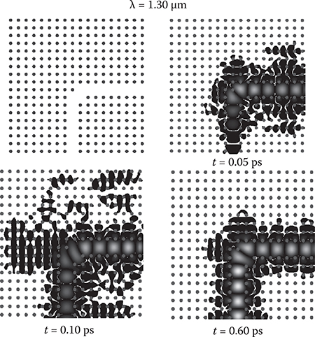
FIGURE 6.30 Transient light beam propagation in a photonic crystal waveguide simulated by the FDTD method. T. Yoshimura, Y. Suzuki, N. Shimoda, T. Kofudo, K. Okada, Y. Arai, and K. Asama, “Three-dimensional chip-scale optical interconnects and switches with self-organized wiring based on device-embedded waveguide films and molecular nanotechnologies,” Proc. SPIE 6126, 612609-1-15 (2006).
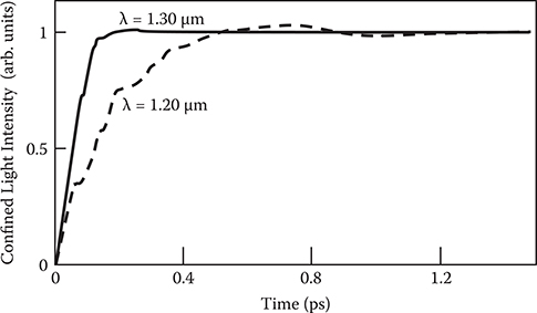
FIGURE 6.31 Transient responses of light beam confinement in a photonic crystal waveguide simulated by the FDTD method.
Connection and integration of the nano-scale optical switches can be done by PL-Pack with SORT, MND, and SOLNET.
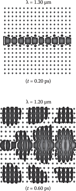
FIGURE 6.32 Light beam distribution in photonic crystal waveguides.
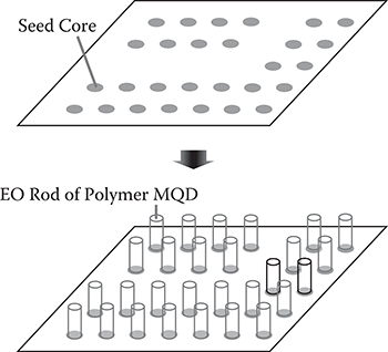
FIGURE 6.33 Concept of a photonic crystal optical switch with the polymer MQD fabricated by MLD.
References
1. T. Yoshimura, S. Tsukada, S. Kawakami, Y. Arai, H. Kurokawa, and K. Asama, “3D micro optical switching system (3D-MOSS) packaging design,” 2001 IEEE LEOS Annual Meeting Conference Proceedings, San Diego, California, 499–500 (2001).
2. T. Yoshimura, S. Tsukada, S. Kawakami, Y. Arai, H. Kurokawa, and K. Asama, “3D micro optical switching system (3D-MOSS) architecture,” Proc. SPIE 4653, from Photonics West 2002, San Jose, California, 62–70 (2002).
3. T. Yoshimura, Waveguide-type electro-optic devices, Japanese Patent Tokukai Hei 4-181231 (1992) [in Japanese].
4. T. Yoshimura, Optical integrated circuit devices, Japanese Patent Tokukai Hei-204633 (1992) [in Japanese].
5. T. Yoshimura, M. Ojima, Y. Arai, and K. Asama, “Three-dimensional self-organized micro optoelectronic systems for board-level reconfigurable optical interconnects: performance modeling and simulation,” IEEE J. Select. Topics in Quantum Electron. 9, 492–511 (2003).
6. T. Yoshimura, S. Tsukada, S. Kawakami, M. Ninomiya, Y. Arai, H. Kurokawa, and K. Asama, “Three-dimensional micro-optical switching system architecture using slab-waveguide-based micro-optical switches,” Opt. Eng. 42, 439–446 (2003).
7. T. Yoshimura, “Design of organic nonlinear optical materials for electro-optic and all-optical devices by computer simulation,” FUJITSU Sc. Tech. J. 27, 115–131 (1991).
8. M. Ninomiya, Y. Arai, T. Yoshimura, H. Kurokawa, and K. Asama, “Characteristics evaluation for waveguide-prism-deflector type micro optical switches (WPD-MOS),” Electronics and Communications in Japan, Part 2 86, 38–48 (2003) [Translated from Denshi Joho Tsushin Gakkai Ronbunshi J85-C, 1192–1201 (2002)].
9. T. Yoshimura, M. Ojima, Y. Arai, N. Fujimoto, and K. Asama, “Simulation on cross-talk reduction in multi-mode-waveguide-based micro optical switching systems using single mode filters,” Appl. Opt. 43, 1390–1395 (2003).
10. T. Yoshimura, and Y. Arai, 3D optoelectronic micro system, U.S. Patent 7,387,913 (2008).
11. O. Qasaimeh, K. Kamath, P. Bhattacharya, and J. Phikkips, “Linear and quadratic electro-optic coefficients of self-organized In0.4Ga0.6As/GaAs quantum dots,” Appl. Phys. Lett. 72, 1275–1277 (1998).
12. T. Yoshimura and T. Futatsugi, Non-linear optical device using quantum dots, U.S. Patent 6,294,794 (2001).
13. T. Yoshimura, “Characterization of the electro-optic effect in styrylpyridinium cyanine dye thin-film crystals by an AC modulation method,” J. Appl. Phys. 62, 2028–2032 (1987).
14. T. Yoshimura, S. Tatsuura, W. Sotoyama, A. Matsuura, and T. Hayano, “Quantum wire and dot formation by chemical vapor deposition and molecular layer deposition of one-dimensional conjugated polymer,” Appl. Phys. Lett. 60, 268–270 (1992).
15. T. Yoshimura, A. Oshima, D. Kim, and Y. Morita, “Quantum dot formation in polymer wires by three-molecule molecular layer deposition (MLD) and applications to electro-optic/photovoltaic devices,” ECS Transactions 25, No. 4 “Atomic layer deposition applications 5,” from the Vienna, Austria Meeting, 15–25 (2009).
16. T. Yoshimura, “Enhancing second-order nonlinear optical properties by controlling the wave function in one-dimensional conjugated molecules,” Phys. Rev. B 40, 6292–6298 (1989).
17. T. Aizawa, Furuuchi Chemical Corporation Technical Articles for PLZT Shutter Arrays.
18. E. Yablonovitch, “Inhibited spontaneous emission in solid state physics and electronics,” Phys. Rev. Lett. 58, 2059–2062 (1987).
19. T. Yoshimura, Y. Suzuki, N. Shimoda, T. Kofudo, K. Okada, Y. Arai, and K. Asama, “Three-dimensional chip-scale optical interconnects and switches with self-organized wiring based on device-embedded waveguide films and molecular nanotechnologies,” Proc. SPIE 6126, from Photonics West 2006, San Jose, California, 612609- 1-15 (2006).