
Appendix D. SDRAM Interface Considerations
At first glance, programming an SDRAM controller can seem like a formidable task. Indeed, there are numerous Synchronous Dynamic Random Access Memory (DRAM) technologies. In a never-ending quest for performance and density, many different architectures and modes of operation have been developed.
We will examine the AMCC PowerPC 405GP processor for this discussion of SDRAM interface considerations. You might want to have a copy of the User’s Manual to reference while we explore the issues related to SDRAM interfacing. This document is referenced in the last section of this appendix.
D.1 SDRAM Basics
To understand SDRAM setup, you must understand the basics of how an SDRAM device operates. Without going into the details of the hardware design, an SDRAM device is organized as a matrix of cells, with a number of address bits dedicated to row addressing, and some dedicated to column addressing, as shown in Figure D-1.
Figure D-1. Simplified SDRAM block diagram

Inside the memory matrix, the circuitry is quite complex. A simplified example of a read operation is as follows: A given memory location is referenced by placing a row address on the row address lines and then placing a column address on the column address lines. After some time has passed, the data stored at the location addressed by the row and column inputs is made available to the processor on the data bus.
The processor outputs a row address on the SDRAM address bus and asserts its Row Address Select (RAS) signal. After a short preprogrammed delay to allow the SDRAM circuitry to capture the row address, the processor outputs a column address and asserts its Column Address Select (CAS) signal. It is the SDRAM controller that translates the actual physical memory address into row and column addresses. Many SDRAM controllers can be configured with the row and column width sizes, and the PPC405GP is one of those examples. Later you will see that this must be configured as part of the SDRAM controller setup.
This example is much simplified, but the concepts are the same. A burst read, for example, reads four memory locations at once and outputs a single RAS and CAS cycle. The internal SDRAM circuitry automatically increments the column address for the subsequent three locations of the burst read, eliminating the need for the processor to issue four separate CAS cycles. This is but one example of performance optimization. The best way to understand this is to absorb the details of an actual memory chip. The last section of this appendix mentions an example of a well-written data sheet.
D.1.1 SDRAM Refresh
An SDRAM is composed of a single transistor and a capacitor. The transistor supplies the charge, and the capacitor’s job is to retain (store) the value of the individual cell. For reasons beyond the scope of this discussion, the capacitor can hold the value for only a short time. One of the fundamental concepts of dynamic memory is that the capacitors representing each cell must be periodically recharged to maintain their value. This is called SDRAM refresh.
A refresh cycle is a special memory cycle that neither reads nor writes data to the memory. It simply performs the required refresh cycle. One of the primary responsibilities of an SDRAM controller is to guarantee that refresh cycles are issued in time to meet the chip’s requirements.
The chip manufacturers specify minimum refresh intervals, and it is the designer’s job to guarantee them. Usually the SDRAM controller can be configured directly to select the refresh interval. The PowerPC 405GP presented here has a register specifically for this purpose. You will read about this shortly.
D.2 Clocking
The term synchronous implies that the data read and write cycles of an SDRAM device coincide with the clock signal from the CPU. Single data rate (SDR) SDRAM is read and written on each SDRAM clock cycle. Dual data rate (DDR) SDRAM is read and written twice on each clock cycle—once on the rising edge of the clock and once on the falling edge.
Modern processors have complex clocking subsystems. Many have multiple clock rates that are used for different parts of the system. A typical processor uses a relatively low-frequency crystal-generated clock source for its primary clock signal. A phase-locked loop (PLL) internal to the processor generates the CPU’s primary clock (the clock rate we speak of when comparing processor speeds). Since the CPU typically runs much faster than the memory subsystem, the processor generates a submultiple of the main CPU clock to feed to the SDRAM subsystem. You need to configure this clocking ratio for your particular CPU and SDRAM combination.
The processor and memory subsystem clocks must be correctly configured for your SDRAM to work properly. Your processor manual contains a section on clock setup and management. You should consult this section for proper setup of your particular board design.
The AMCC 405GP is typical of processors because of its feature set. It takes a single crystal-generated clock input source and generates several internal and external clocks required of its subsystems. It generates clocks for the CPU, PCI interface, Onboard Peripheral Bus (OPB), Processor Local Bus (PLB), Memory Clock (MemClk), and several internal clocks for peripherals such as the timer and UART blocks. Table D-1 shows what a typical configuration might look like.
Table D-1. Sample Clock Configuration
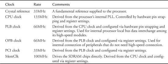
Decisions about clock setup normally must be made at hardware design time. Pin strapping options determine initial clock configurations upon application of power to the processor. You often can get some control over derived clocks by setting divider bits accessible through processor internal registers dedicated to clock and subsystem control. In the example we present here based on the 405GP, final clock configuration is determined by pin strapping and firmware configuration. It is the bootloader’s responsibility to set the initial dividers and any other clock options that can be configured via processor register bits very early after power is applied.
D.3 SDRAM Setup
After the clocks have been configured, the next step is to configure the SDRAM controller. Controllers vary widely from processor to processor, but the end result is always the same: You must provide the correct clocking and timing values to enable and optimize the performance of the SDRAM subsystem.
As with other material in this book, there is no substitute for detailed knowledge of the hardware you are trying to configure. This is especially true for SDRAM. It is beyond the scope of this appendix to explore the design of SDRAM, but you need to understand some basics. Many manufacturers’ data sheets on SDRAM devices contain helpful technical descriptions. You are urged to familiarize yourself with the content of these data sheets. You don’t need a degree in hardware engineering to understand what you must do to properly configure your SDRAM subsystem, but you need to achieve some level of understanding.
We will examine how the SDRAM controller is configured on the 405GP processor as configured by the U-Boot bootloader we covered in Chapter 7, “Bootloaders.” Recall from Chapter 7 that U-Boot provides a hook for SDRAM initialization from the assembly language startup code found in start.S in the 4xx-specific CPU directory. Refer to Section 7.4.5, “Board-Specific Initialization,” in Chapter 7. Listing D-1 shows the sdram_init() function from U-Boot’s .../cpu/ppc4xx/sdram.c file.
Listing D-1. ppc4xx sdram_init() from U-Boot
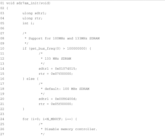
The first action reads the pin strapping on the 405GP processor to determine the design value for the SDRAM clock. In this case, we can see that two possible values are accommodated: 100MHz and 133MHz. Based on this choice, constants are chosen that will be used later in the function to set the appropriate register bits in the SDRAM controller.
Starting on line 24, a loop is used to set the parameters for each of up to five predefined memory sizes. Currently U-Boot has logic to support a single bank of memory sized at one of 4MB, 16MB, 32MB, 64MB, or 128MB. These sizes are defined in a table called mb0cf in .../cpu/ppc4xx/sdram.c. The table associates a constant with each of these memory sizes, based on the value required in the 405GP memory bank configuration register. The loop does this:

This simple logic simply plugs in the correct timing constants in the SDRAM controller based on SDRAM clock speed and configured memory bank size from the hard-coded table in U-Boot. Using this explanation, you can easily correlate the bank configuration values using the 405GP reference manual. For a 64MB DRAM size, the memory bank control register is set as follows:
Memory Bank 0 Control Register = 0x000a4001
The PowerPC 405GP User’s Manual describes the fields shown in Table D-2 for the memory bank 0 control register.
Table D-2. 405GP Memory Bank 0-3 Configuration Register Fields
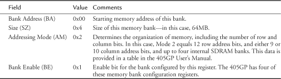
The designer must determine the values in this table based on the memory module in use on the board.
Let’s look at a timing example to see more details on the timing requirements of a typical SDRAM controller. Assuming a 100MHz SDRAM clock speed and 64MB memory size, the timing constants selected by the sdram_init() function in Listing D-1 are selected as follows:
![]()
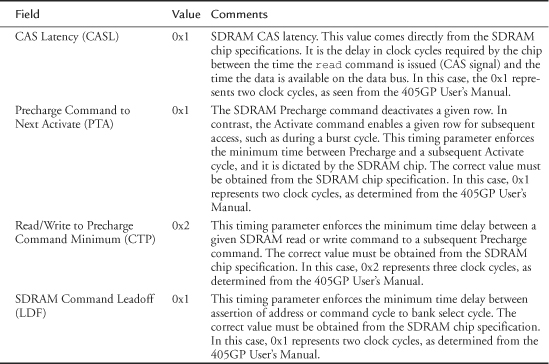
The PowerPC 405GP User’s Manual describes the fields shown in Table D-3 for the SDRAM Timing Register.
Table D-3. 405GP SDRAM Timing Register Fields
The final timing parameter configured by the U-Boot example in Listing D-1 is the refresh timing register value. This register requires a single field that determines the refresh interval enforced by the SDRAM controller. The field representing the interval is treated as a simple counter running at the SDRAM clock frequency. In the example here, we assume 100MHz as the SDRAM clock frequency. The value programmed into this register in our example is 0x05f0_0000. From the PowerPC 405GP User’s Manual, we determine that this will produce a refresh request every 15.2 microseconds. As with the other timing parameters, this value is dictated by the SDRAM chip specifications.
A typical SDRAM chip requires one refresh cycle for each row. Each row must be refreshed in the minimum time specified by the manufacturer. In the chip referenced in the final section of this appendix, the manufacturer specifies that 8,192 rows must be refreshed every 64 milliseconds. This would require generating a refresh cycle every 7.8 microseconds to meet the specifications for this particular device.
D.4 Summary
SDRAM devices are complex. This appendix presented a simple example to help you navigate the complexities of SDRAM controller setup. The SDRAM controllers perform a critical function, and they must be set up properly. There is no substitute for diving into a specification and digesting the information presented. The two sample documents referenced in this appendix are an excellent starting point.
D.4.1 Suggestions for Additional Reading
AMCC 405GP Embedded Processor User’s Manual
AMCC Corporation
www.amcc.com/Embedded/
Micron Technology, Inc.
Synchronous DRAM MT48LC64M4A2 Data Sheet
http://download.micron.com/pdf/datasheets/dram/sdram/256MSDRAM.pdf