
Chapter 6
Efficiency Enhancement of Organic Light‐Emitting Diodes Exhibiting Delayed Fluorescence and Nonisotropic Emitter Orientation
Tobias D. Schmidt and Wolfgang Brütting
University of Augsburg, Institute of Physics, Augsburg, 86135, Germany
6.1 Introduction
In 1963 the first observation of electroluminescence (EL) of a 5 mm thick anthracene crystal was presented by Pope et al. [1]. Thereafter, it took more than 20 years until Tang and van Slyke demonstrated the first efficient, low‐voltage‐driven, thin film organic light‐emitting diode (OLED) in 1987 [2]. Three years later the first solution processed polymer‐based OLED was developed by Burroughes et al. [3] and therewith the starting signal for a new, rapidly growing field of research had been given. These early OLEDs used fluorescent (so‐called first‐generation) emitter materials, which have the fundamental limitation that only singlet excitons, and, thus, only 25% of all electrically excited states are able to decay radiatively producing photons [4]. In 1998, Baldo et al. [5] presented the first OLED with nearly 100% internal quantum efficiency where they used phosphorescent emitters for the first time. In this second‐generation emitter materials, the energy of all excited states is finally transferred to triplet states that show efficient radiative decay with lifetimes in the (sub)microsecond regime [6].
In the last few years, technologies based on OLEDs made tremendous progress [7], [8]. Nowadays, several applications using OLEDs are commercially available, e.g. in the general lighting sector as well as in the display market, especially, for smartphones and tablet computers. However, most of the commercial applications for white light emission are still using hybrid stack systems with a fluorescent blue and phosphorescent red and green emitting materials, because sufficiently stable and efficient phosphorescent molecules in the blue spectral range are still challenging [9], [10]. Thus, a promising new class of emitting compounds is coming more and more into the focus of the OLED community, namely, devices incorporating delayed fluorescence (so‐called third‐generation) emitter materials [11].
Delayed fluorescence can be enabled by two different mechanisms, viz triplet–triplet annihilation (TTA) [12]–[18] and thermally activated delayed fluorescence (TADF) [11], [19]–[26], originally termed p‐ and e‐type delayed fluorescence [27], [28]. Although their working principles differ in detail, both phenomena increase device efficiency compared to standard fluorescent OLEDs and sometimes even reach the efficiency of phosphorescent applications by recycling triplet excitons and converting them into singlet excited states[29]–[32].
In many cases, however, we find that arguments related to spin multiplicity of the excited states alone (and their potential interconversion by these processes) are not sufficient to explain the observed efficiency boost enabled by these materials. Rather, some of the emitter molecules exhibit a strongly nonisotropic distribution of their optical transition dipole vectors (TDVs), which in the case of horizontal alignment is additionally increasing the light output from these OLEDs [33]. Therefore, this chapter aims at giving the required background for a thorough efficiency analysis of OLEDs disentangling both effects and presents exemplary case studies of OLEDs exhibiting these features. In the context of this article, we restrict ourselves to purely organic emitter materials; however, most of the statements are equally valid for metal–organic complexes containing e.g. Cu(I).
6.2 OLED Basics
6.2.1 Working Principle
For the sake of simplicity, we will elucidate the basic operation processes for the simplest OLED only consisting of one organic layer sandwiched between two electrodes (see Figure 6.1). In order to facilitate light emission to the outside world of the OLED, one of these two electrodes has to be (semi)transparent, e.g. a thin indium tin oxide (ITO) anode on a glass substrate. The most important energy values in such a simplified device are the work functions of the used electrodes and the highest occupied molecular orbital (HOMO) as well as the lowest unoccupied molecular orbital (LUMO) of the organic solid. The work functions of anode and cathode should be close to the positions of the HOMO and the LUMO levels, respectively, in order to enable charge carrier injection from the electrodes into the organic material.
In Figure 6.1 a schematic sketch of the important energy levels and the four different steps required for light emission are illustrated [7], [34], [35]. First, electrons are injected from the cathode side to the LUMO of the organic material, while simultaneously electrons are extracted at the anode side from the HOMO of the organic material (or in other words holes are injected into the HOMO) as soon as a sufficiently high external voltage is applied to the electrodes. Second, due to the external applied electric field, the charges are transported toward the electrode with the opposite polarity. Third, if electrons and holes come close enough together – less than the Coulomb radius – on their way through the OLED, they will recombine under the generation of an exciton, which describes a bound excited state on one organic molecule. Finally, the exciton can decay radiatively under creation of a photon, which can thereafter be extracted to the outside world of the OLED.
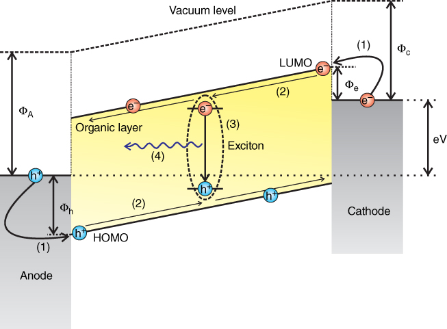
Figure 6.1 Simplified illustration of a single‐layer OLED stack. In order to obtain charge carrier injection and subsequent light emission, an external voltage is applied to the electrodes. Light emission occurs following four subsequent steps: (1) charge carrier injection, (2) charge carrier transport, (3) charge carrier recombination, generating an exciton, and, finally, (4) radiative decay of the exciton creating a (visible) photon.
State‐of‐the‐art OLEDs, of course, use more than one organic material to improve device performance [36]. There are several different layers, each with special properties. Thus, a typical OLED stack, as depicted in Figure 6.2, starts with an ITO anode on a glass substrate, subsequently followed by a (conductivity‐doped) hole transport layer (HTL) and the emission layer (EML) consisting of two or sometimes even three different materials forming a so‐called guest/host system. On top, the (conductivity‐doped) electron transport layer (ETL) and a metallic cathode are completing the OLED structure electrically, and an encapsulation protects it from atmospheric moisture and oxygen. Often, the ETL and the HTL are simultaneously acting as blocking layer for the oppositely charged carrier species (HBL and EBL, respectively). In this case a small region next to the EML is not conductivity doped to avoid exciton quenching processes.

Figure 6.2 Simplified illustration of a three‐layer OLED stack with an emission layer containing three subunits emitting light in different color. The light emission process from the excited state of a molecule can be described as electric dipole radiation with a characteristic emission pattern depending on the direction of the transition dipole vector (TDV).
6.2.2 Electroluminescence Quantum Efficiency
The most important figure to benchmark OLEDs is the electroluminescence (or external) quantum efficiency (EQE), which is defined as the number of emitted photons divided by the number of injected charges and is given by four individual factors [4]:
Therein, the first three factors yield the internal quantum efficiency ![]() , giving the fraction of produced photons per injected carriers that are available for being extracted from the thin film structure, as quantified by the light‐outcoupling factor
, giving the fraction of produced photons per injected carriers that are available for being extracted from the thin film structure, as quantified by the light‐outcoupling factor ![]() .
.
The factor ![]() represents the charge carrier balance of the device. Only if every electron finds a hole to recombine with (and vice versa), this value becomes unity. In state‐of‐the‐art OLEDs, using appropriate transport and blocking layers
represents the charge carrier balance of the device. Only if every electron finds a hole to recombine with (and vice versa), this value becomes unity. In state‐of‐the‐art OLEDs, using appropriate transport and blocking layers ![]() can be assumed to be close to one [37], [38].
can be assumed to be close to one [37], [38].
Next, ![]() stands for the radiative exciton fraction and is determined by quantum‐mechanical selection rules. In first approximation, only excitons with total spin equal to zero (singlet excitons) are allowed to decay radiatively. By contrast, excited states with total spin 1 (triplet excitons) can only decay nonradiatively. This selection rule can be overcome if spin–orbit coupling is strong for the excited molecule, such as for phosphorescent metal–organic complexes based on heavy metal central atoms, e.g., iridium or platinum [6]. However, for ordinary fluorescent molecules the spin–orbit coupling is too weak to change this selection rule significantly at room temperature.
stands for the radiative exciton fraction and is determined by quantum‐mechanical selection rules. In first approximation, only excitons with total spin equal to zero (singlet excitons) are allowed to decay radiatively. By contrast, excited states with total spin 1 (triplet excitons) can only decay nonradiatively. This selection rule can be overcome if spin–orbit coupling is strong for the excited molecule, such as for phosphorescent metal–organic complexes based on heavy metal central atoms, e.g., iridium or platinum [6]. However, for ordinary fluorescent molecules the spin–orbit coupling is too weak to change this selection rule significantly at room temperature.
The third factor ![]() is the effective radiative quantum efficiency (RQE) of the emitting system. It depends on the competition between radiative and nonradiative decay channels in the excited state, whereby the transition rate for the former is modified via the Purcell effect by the photonic density of states in an OLED microcavity (for details see Refs [39]–[43]). Additionally, in an electrically operating OLED, this factor decreases at high current densities due to nonradiative exciton quenching processes [44]–[47]. We want to emphasize here in the context of delayed fluorescence emitters that
is the effective radiative quantum efficiency (RQE) of the emitting system. It depends on the competition between radiative and nonradiative decay channels in the excited state, whereby the transition rate for the former is modified via the Purcell effect by the photonic density of states in an OLED microcavity (for details see Refs [39]–[43]). Additionally, in an electrically operating OLED, this factor decreases at high current densities due to nonradiative exciton quenching processes [44]–[47]. We want to emphasize here in the context of delayed fluorescence emitters that ![]() stands for (spontaneous) radiative decay processes from singlet excited states. Changes in their population by TADF or TTA would not change this value but enter only in the radiative exciton fraction
stands for (spontaneous) radiative decay processes from singlet excited states. Changes in their population by TADF or TTA would not change this value but enter only in the radiative exciton fraction ![]() .
.
Finally, the remaining factor ![]() is the light‐outcoupling efficiency, which quantifies how many photons are actually able to leave the OLED through the transparent electrode without being trapped and dissipated in waveguided modes or surface plasmons or simply being reabsorbed. Depending, of course, on the details of the OLED layer stack, this fraction is typically around 20% for emissive dipoles with random orientation [42], [43]. Note that the light that is trapped in the glass substrate can easily be extracted by microlense arrays or scattering particles [48] and is, thus, not being considered as a loss channel.
is the light‐outcoupling efficiency, which quantifies how many photons are actually able to leave the OLED through the transparent electrode without being trapped and dissipated in waveguided modes or surface plasmons or simply being reabsorbed. Depending, of course, on the details of the OLED layer stack, this fraction is typically around 20% for emissive dipoles with random orientation [42], [43]. Note that the light that is trapped in the glass substrate can easily be extracted by microlense arrays or scattering particles [48] and is, thus, not being considered as a loss channel.
As a result, the classical efficiency limits for OLEDs with first‐ and second‐generation emitter materials are given as
6.2.3 Delayed Fluorescence
In the simple spin statistical picture, ![]() does not include effects like TTA and TADF, changing the fraction of singlet excited states after charge carrier recombination [5], [7], [11], [49]–[52]. Figure 6.3 illustrates the schematic mechanisms behind both processes resulting in delayed fluorescence and therewith an enhanced radiative exciton fraction.
does not include effects like TTA and TADF, changing the fraction of singlet excited states after charge carrier recombination [5], [7], [11], [49]–[52]. Figure 6.3 illustrates the schematic mechanisms behind both processes resulting in delayed fluorescence and therewith an enhanced radiative exciton fraction.
In the case of TADF, the exchange energy between the first excited singlet (![]() ) and triplet state (
) and triplet state (![]() ) is in the range of the thermal energy (or a few times
) is in the range of the thermal energy (or a few times ![]() ) resulting in a back transfer – i.e. reverse intersystem crossing (rISC) – of triplet into singlet excitons. As this process is slow compared with the prompt emission from singlet excitons generated by direct charge carrier recombination, a delayed fluorescence can be observed. For sufficiently low singlet–triplet splitting and high enough temperatures, this mechanism can theoretically result in a radiative exciton fraction of unity like for phosphorescent emitters [5], [7], [11], [49]–[52].
) resulting in a back transfer – i.e. reverse intersystem crossing (rISC) – of triplet into singlet excitons. As this process is slow compared with the prompt emission from singlet excitons generated by direct charge carrier recombination, a delayed fluorescence can be observed. For sufficiently low singlet–triplet splitting and high enough temperatures, this mechanism can theoretically result in a radiative exciton fraction of unity like for phosphorescent emitters [5], [7], [11], [49]–[52].
In contrast, TTA cannot reach this high value for ![]() , because it is a bimolecular process where at least one triplet is lost instead of forming the desired singlet excited state [35], [53], [54]. TTA takes place if two excited triplet states encounter each other on neighboring molecules, where, in the ideal case, they form one singlet excited state (
, because it is a bimolecular process where at least one triplet is lost instead of forming the desired singlet excited state [35], [53], [54]. TTA takes place if two excited triplet states encounter each other on neighboring molecules, where, in the ideal case, they form one singlet excited state (![]() ) and one ground state (S
) and one ground state (S![]() ) [53]:
) [53]:
For this to happen, the excited ![]() state must at least have half of the excitation energy of the corresponding
state must at least have half of the excitation energy of the corresponding ![]() state
state ![]() . The so generated excited singlet state can thereafter decay under light emission and can be detected as delayed fluorescence. Thus, ideally one‐half of the (originally) nonemissive triplet excitons can be recycled as singlet excitons, leading to an upper limit for the radiative exciton fraction of
. The so generated excited singlet state can thereafter decay under light emission and can be detected as delayed fluorescence. Thus, ideally one‐half of the (originally) nonemissive triplet excitons can be recycled as singlet excitons, leading to an upper limit for the radiative exciton fraction of ![]() [13]. However, there is another pathway for TTA that does not result in an excited singlet state and delayed fluorescence, but just in a deactivation of one of the two triplet excitons:
[13]. However, there is another pathway for TTA that does not result in an excited singlet state and delayed fluorescence, but just in a deactivation of one of the two triplet excitons:
Basically, the energy of the two triplets is used to excite one of both to a higher‐lying triplet state (![]() ,
, ![]() ,
, ![]() , …) relaxing by internal conversion again to the first excited triplet state without enhancing the radiative exciton fraction. This can be a loss channel in both fluorescent and phosphorescent OLEDs at high current density [45]–[47], [55], [56]. Furthermore, TTA is an unwanted decay channel for TADF emitting systems as it is reducing the amount of excited triplet states. We note that, in principle, two triplets with spin 1 each can form not only entities with total spin 0 (
, …) relaxing by internal conversion again to the first excited triplet state without enhancing the radiative exciton fraction. This can be a loss channel in both fluorescent and phosphorescent OLEDs at high current density [45]–[47], [55], [56]. Furthermore, TTA is an unwanted decay channel for TADF emitting systems as it is reducing the amount of excited triplet states. We note that, in principle, two triplets with spin 1 each can form not only entities with total spin 0 (![]() ) and 1 (
) and 1 (![]() ) but also a quintet state with total spin 2 (
) but also a quintet state with total spin 2 (![]() ), but due to its high energy, this process is usually not relevant [53].
), but due to its high energy, this process is usually not relevant [53].

Figure 6.3 Simplified illustration of the underlying mechanisms of (a) thermally activated delayed fluorescence (TADF) and (b) triplet–triplet annihilation (TTA) enhancing the radiative exciton fraction in fluorescent materials after charge carrier recombination. For TADF materials, the exchange energy between the first excited singlet ( ) and triplet state (
 ) is in the range of the thermal energy enabling the back transfer from the triplet to the singlet state resulting in delayed fluorescence. For the TTA process, two excited triplet states interact ideally forming one excited singlet and one ground state (
 ) leading to delayed fluorescence, too.
6.2.4 Nonisotropic Emitter Orientation
Nonisotropic emitter orientation, i.e. horizontal alignment of the TDVs with respect to the substrate plane, is a powerful tool to increase OLED efficiency [33], [43], [57]–[59]. Treating the radiative transitions as classical oscillating dipoles (see Figure 6.2) makes it obvious that horizontal orientation is the preferred alignment for enhanced light outcoupling due to the fact that a dipole emits most of the energy perpendicular to its axis. Hence, the outcoupling factor can be significantly increased from ca. ![]() (for the isotropic case) to over
(for the isotropic case) to over ![]() (when perfectly horizontal alignment is achieved) in standard devices [43], [59] or from
(when perfectly horizontal alignment is achieved) in standard devices [43], [59] or from ![]() to even
to even ![]() if very thin ITO anodes and birefringent transport layers are used [60], [61]. Noteworthy, such high values are attained without using (complex) outcoupling enhancements such as nanostructured electrodes [62] or scattering particles [48].
if very thin ITO anodes and birefringent transport layers are used [60], [61]. Noteworthy, such high values are attained without using (complex) outcoupling enhancements such as nanostructured electrodes [62] or scattering particles [48].
To have a measure quantifying the degree of anisotropy for the TDVs of an emissive guest/host system, the orientation parameter ![]() is defined as the ratio of energy radiated by vertically aligned transition dipole moments to the total radiated power [43], [59], [63]. Based on this definition an isotropic distribution of the TDVs results in a
is defined as the ratio of energy radiated by vertically aligned transition dipole moments to the total radiated power [43], [59], [63]. Based on this definition an isotropic distribution of the TDVs results in a ![]() value of 0.33, a perfect horizontal alignment is identified by
value of 0.33, a perfect horizontal alignment is identified by ![]() , and a completely vertical orientation yields
, and a completely vertical orientation yields ![]() .
.
In general the connection between ![]() and an ensemble of molecules, each having different possible orientations of the TDVs, is
and an ensemble of molecules, each having different possible orientations of the TDVs, is

where ![]() denotes the relative contribution of each dye molecule,
denotes the relative contribution of each dye molecule, ![]() describes the relative contribution of the
describes the relative contribution of the ![]() th transition dipole moment
th transition dipole moment ![]() on the
on the ![]() th molecule, and
th molecule, and ![]() denotes the vertical component of the corresponding TDV [64].
denotes the vertical component of the corresponding TDV [64].
6.2.5 Optical Modeling
In this chapter we use optical modeling for a comprehensive efficiency analysis of OLEDs exhibiting delayed fluorescence and nonisotropic emitter orientation. Here we summarize only the most important concepts; for a detailed discussion we refer to the literature [41–43, 59].
Light emission in OLEDs is treated as dipole radiation of an ensemble of incoherent emitters embedded in a weak microcavity formed by the substrate and the multilayer stack [40]. Depending on the details of the used layers, such as their thicknesses, their optical constants, the emission spectrum, and the position as well as the orientation of the emissive dipoles, the EQE of an OLED is affected in two ways by the optical cavity via the product ![]() .
.
First, the radiative decay rate (![]() ) from the excited state is modified by the Purcell effect [39, 40, 65], i.e. the coupling to the photonic density of states of the cavity, while the nonradiative decay rate (
) from the excited state is modified by the Purcell effect [39, 40, 65], i.e. the coupling to the photonic density of states of the cavity, while the nonradiative decay rate (![]() ) is not affected. Thus, the “free‐space” value of the RQE
) is not affected. Thus, the “free‐space” value of the RQE ![]() of the emitter in the given host is modified by introducing the Purcell factor
of the emitter in the given host is modified by introducing the Purcell factor ![]() acting on the radiative rate to yield the effective RQE for a given OLED cavity [66]:
acting on the radiative rate to yield the effective RQE for a given OLED cavity [66]:

This, of course, also modifies the excited state lifetime ![]() with respect to its value in an infinite medium consisting of the dye and the matrix material
with respect to its value in an infinite medium consisting of the dye and the matrix material ![]() [63]:
[63]:

Second, depending on the cavity length and, in particular, on the distance ![]() of the emitter to the highly reflecting metallic back electrode and on the emitter orientation
of the emitter to the highly reflecting metallic back electrode and on the emitter orientation ![]() , the generated optical power is redistributed between different optical modes. In this context, the light‐outcoupling factor
, the generated optical power is redistributed between different optical modes. In this context, the light‐outcoupling factor ![]() quantifies the fraction of the desired direct light emission that leaves the OLED through the transparent substrate
quantifies the fraction of the desired direct light emission that leaves the OLED through the transparent substrate ![]() with respect to all generated optical power
with respect to all generated optical power ![]() inside the OLED stack [43]:
inside the OLED stack [43]:

Therefore, the total power ![]() is given by integrating the position‐ and orientation‐dependent power dissipation spectrum
is given by integrating the position‐ and orientation‐dependent power dissipation spectrum ![]() of the dipoles inside the cavity over all in‐plane wave vectors
of the dipoles inside the cavity over all in‐plane wave vectors ![]() and all wavelengths
and all wavelengths ![]() with the emission spectrum
with the emission spectrum ![]() as weighting function:
as weighting function:

where the double integral at the same time is the definition of the Purcell factor ![]() , which – to emphasize this point again – depends particularly on the position
, which – to emphasize this point again – depends particularly on the position ![]() of the emitter in the cavity and its orientation
of the emitter in the cavity and its orientation ![]() . The actually outcoupled fraction is obtained from a similar expression, where the integration over
. The actually outcoupled fraction is obtained from a similar expression, where the integration over ![]() is only performed over the accessible light‐output cone, e.g. for direct and/or substrate emission.
is only performed over the accessible light‐output cone, e.g. for direct and/or substrate emission.
For the following, it is important to recall that the RQE (![]() ) is an intrinsic property of the emissive system, i.e. the dye and its dielectric environment (the matrix where the dye is embedded in with a certain concentration), which is independent of the cavity. The effective RQE
) is an intrinsic property of the emissive system, i.e. the dye and its dielectric environment (the matrix where the dye is embedded in with a certain concentration), which is independent of the cavity. The effective RQE ![]() , however, is the particular value of the RQE for a given OLED stack, where the emitter has a certain position and orientation. Thus, when we systematically change the emitter position by a layer thickness variation, the whole series of OLEDs is characterized by a single value of
, however, is the particular value of the RQE for a given OLED stack, where the emitter has a certain position and orientation. Thus, when we systematically change the emitter position by a layer thickness variation, the whole series of OLEDs is characterized by a single value of ![]() , while both
, while both ![]() and
and ![]() are layer thickness and orientation dependent.
are layer thickness and orientation dependent.
6.3 Comprehensive Efficiency Analysis of OLEDs
For a comprehensive efficiency analysis of OLEDs, one needs to determine the four individual factors of the external quantum efficiency separately from each other [44, 63, 67]. The first problem hereby is that at the moment there exists no method to determine the charge carrier balance ![]() of a device accurately. However, if appropriate blocking layers and conductivity‐doped transport layers are used, this factor can be assumed to be very close to unity in state‐of‐the‐art OLEDs [36]. In contrast to phosphorescent emitting systems, where the radiative exciton fraction can also be assumed as
of a device accurately. However, if appropriate blocking layers and conductivity‐doped transport layers are used, this factor can be assumed to be very close to unity in state‐of‐the‐art OLEDs [36]. In contrast to phosphorescent emitting systems, where the radiative exciton fraction can also be assumed as ![]() , for delayed fluorescence, one has to determine all three remaining factors contributing to the EL quantum efficiency, namely,
, for delayed fluorescence, one has to determine all three remaining factors contributing to the EL quantum efficiency, namely, ![]() ,
, ![]() (or
(or ![]() in the OLED cavity), and
in the OLED cavity), and ![]() . Thus, three independent experiments are performed on a set of OLEDs with the same emitting system but having different distances of their EML to the metallic mirror of the device (typically by variable ETL thicknesses) in order to get access to the unknown parameters (see Figure 6.4 for a graphical illustration):
. Thus, three independent experiments are performed on a set of OLEDs with the same emitting system but having different distances of their EML to the metallic mirror of the device (typically by variable ETL thicknesses) in order to get access to the unknown parameters (see Figure 6.4 for a graphical illustration):
- Time‐resolved EL and/or photoluminescence (PL) spectroscopy.
- Polarized angular dependent emission spectroscopy under steady‐state conditions.
- External quantum efficiency measurements without and with macroextractor (at sufficiently low current densities to avoid current‐induced quenching processes).

Figure 6.4 Illustration of the three different measurement techniques combined for a comprehensive efficiency analysis (the shown experimental and simulation data are taken from an investigation of a red phosphorescent emitting system). (a) Time‐resolved electroluminescence (EL) and/or photoluminescence (PL) spectroscopy using a streak camera system to get access to the excited‐state lifetimes of the emitting system for different interference conditions inside a microcavity. (b) Polarized angular dependent emission spectroscopy under steady‐state conditions to determine the orientation parameter of the emitting system. (c) External quantum efficiency measurements without and with macroextractor for different emitter‐to‐cathode distances. In case of (a) and (c), the distance between the emitting and the metal layer is systematically varied.
Source: Ref. [43]. Reproduced with permission of John Wiley & Sons.
Time‐resolved EL and PL spectroscopy is a powerful tool to analyze excitonic processes in OLEDs. For phosphorescent emitting systems, EL and PL should basically yield the same information; however, differences can arise due to the fact that the spatial exciton generation profile for optical and electrical excitation can be different: PL usually probes a more or less uniformly excited EML, whereas EL originates from a spatially inhomogeneous recombination profile, and EL is affected by exciton quenching processes at high currents [46, 68]. Thus, often electrical excitation is the better choice to determine the excited‐state lifetime of the guest/host system, as it is closer to the real situation during electrical operation. The situation is somewhat different for fluorescent dyes, because the prompt decay time is typically much shorter than the RC time of the actual device and, hence, cannot be resolved with electrical excitation. In this case, the prompt decay can only be detected by optical excitation, if a suitable detection window (typically in the ns range) is chosen. On the other hand, mechanisms such as TTA or TADF will lead to delayed fluorescence signals (typically in the microsecond range), which can be observed by both PL and EL measurements. However, time‐resolved EL has the advantage that a quantitative estimation of the relative contributions of both prompt and delayed fluorescence is possible, yielding direct information on the radiative exciton fraction ![]() [13]. Furthermore, laser excitation does not directly populate the triplet states of the emitting molecules (except for special cases as Cu(I) complexes), in contrast to electrical excitation where three triplet excitons are created for each singlet exciton. Hence, delayed fluorescence signals are typically weaker in a PL experiment compared with an EL investigation.
[13]. Furthermore, laser excitation does not directly populate the triplet states of the emitting molecules (except for special cases as Cu(I) complexes), in contrast to electrical excitation where three triplet excitons are created for each singlet exciton. Hence, delayed fluorescence signals are typically weaker in a PL experiment compared with an EL investigation.
As mentioned before, the Purcell effect strongly affects the effective radiative rate of the emitting system as a function of the cavity length, i.e. the distance of the emitter from the mirror‐like metallic cathode. However, this is only true for the prompt decay but not the delayed component, because intersystem crossing (ISC) and rISC are not affected by the photon field in the OLED cavity and are acting on completely different time scales as the direct singlet emission. Thus, from a systematic variation of the OLED ETL thickness, it is possible to determine the RQE of the emitting system by comparing the oscillation of the excited‐state lifetime of the prompt decay with numerical simulations (see Figure 6.4a).
As has been shown by simulation, the Purcell factor exhibits a certain dependence on the orientation of the transition dipole moments of the emitting species [59, 63, 69]. Thus, the knowledge of the emitter orientation is a crucial point to ensure a consistent determination of the emitter's effective RQE inside the OLED stack. Therefore, polarization‐ and angular‐dependent PL emission pattern analysis is performed for the guest/host system under investigation and is then compared with optical simulations yielding the orientation parameter ![]() (see Figure 6.4b). Here, two different experiments are possible. First, the analysis can be applied to a simplified stack only consisting of a thin layer (≈10 nm) of the guest/host system on a glass substrate attached to a half‐cylinder prism extracting the substrate modes, which is connected to a rotary stage. The film is then excited with an ultraviolet laser diode (375 nm), and the p‐polarized emission containing contributions of both, vertical and horizontal TDVs, is detected as a function of the emission angle [70]. Alternatively, one can extract the orientation parameter from a complete OLED stack where the emitting system is positioned in the first node of the OLED cavity (at a distance
(see Figure 6.4b). Here, two different experiments are possible. First, the analysis can be applied to a simplified stack only consisting of a thin layer (≈10 nm) of the guest/host system on a glass substrate attached to a half‐cylinder prism extracting the substrate modes, which is connected to a rotary stage. The film is then excited with an ultraviolet laser diode (375 nm), and the p‐polarized emission containing contributions of both, vertical and horizontal TDVs, is detected as a function of the emission angle [70]. Alternatively, one can extract the orientation parameter from a complete OLED stack where the emitting system is positioned in the first node of the OLED cavity (at a distance ![]() of the emission peak wavelength from the metallic cathode if the refractive index of the organic material is close to 2) with the same procedure as mentioned for the former method [71] by using electrical excitation. And, OLED stacks without metallic cathode can be investigated by PL spectroscopy, too. Note that it is mandatory to determine the exact layer thicknesses and optical constants for all used layers and to take into account possible anisotropies of the refractive indices (birefringence) to ensure an appropriate analysis.
of the emission peak wavelength from the metallic cathode if the refractive index of the organic material is close to 2) with the same procedure as mentioned for the former method [71] by using electrical excitation. And, OLED stacks without metallic cathode can be investigated by PL spectroscopy, too. Note that it is mandatory to determine the exact layer thicknesses and optical constants for all used layers and to take into account possible anisotropies of the refractive indices (birefringence) to ensure an appropriate analysis.
However, nonisotropic emitter orientation is crucial not only for the changes of the excited state lifetime for varying emitter‐to‐cathode distances but also for the overall outcoupling efficiency of the device as a function of the ETL thickness. Thus, in order to complete the efficiency analysis, EL quantum efficiency measurements, again for a set of OLEDs with varying ETL thickness, in a calibrated integrating sphere (see Figure 6.4c) have to be performed for a sufficiently low current density to avoid current‐induced quenching effects [44]. Note that measuring the zero degree emission intensity and weighting the obtained results with a lambertian emission profile is not an appropriate way to determine EQE values as, e.g. for nonisotropic emitter orientation the emission pattern can deviate from the lambertian case.
In principle, EQE measurements with systematically varied cavity length are sufficient to determine ![]() and
and ![]() in phosphorescent OLEDs [71], however, if no macroextractor is used, ambiguities concerning the orientation parameter
in phosphorescent OLEDs [71], however, if no macroextractor is used, ambiguities concerning the orientation parameter ![]() and thus
and thus ![]() can arise [72]. Thus, it is mandatory to measure EQEs in both configurations (i.e. direct emission from the plane glass substrate and substrate mode emission using a macroextractor) [73]. This becomes even more important in the fluorescent case, as there are three individual factors determining the EQE. As will be seen in the following examples, information obtained from different experiments, as mentioned above, have to be combined to yield reliable results.
can arise [72]. Thus, it is mandatory to measure EQEs in both configurations (i.e. direct emission from the plane glass substrate and substrate mode emission using a macroextractor) [73]. This becomes even more important in the fluorescent case, as there are three individual factors determining the EQE. As will be seen in the following examples, information obtained from different experiments, as mentioned above, have to be combined to yield reliable results.
6.4 Case Studies
6.4.1 Treating the OLED as a Black Box
In this first example, we had a series of blue fluorescent OLEDs at hand [67], where only the stack layout as shown in Figure 6.5a including layer thicknesses, optical constants, and the emission spectrum, but no details of the used materials were known. In that sense this state‐of‐the‐art blue fluorescent OLEDs are kind of a “black box,” which will be used in the following to demonstrate how a comprehensive efficiency analysis has to be performed. The OLEDs exhibit an external quantum efficiency of about 5% for optimized layer thickness, which is the classical limit for a fluorescent device, if one assumes ![]() ,
, ![]() ,
, ![]() , and
, and ![]() .
.

Figure 6.5 (a) Stack layout of a blue fluorescent OLED with varying ETL thickness. (b) External quantum efficiency measurements for direct emission (squares) and with a macroextractor attached to the substrate (dots) at a current density of 2 mA cm . The solid lines represent optical simulations for isotropic emitter orientation and an assumed radiative exciton fraction of 25%, a charge carrier balance of unity, and a radiative quantum efficiency of 100%.
Source: Ref. [67]. Reproduced with permission of AIP Publishing LLC.
Figure 6.5 b illustrates the measured EQE values for varying ETL thickness for direct emission and with a macroextractor (half‐ball lens) attached to the substrate giving access to the captured substrate modes. As mentioned before, for thickness optimized devices the EQE for direct emission reaches 5% for ETL thicknesses of 31 and 184 nm, respectively. Although it is possible to simulate the EQE for direct emission with isotropic emitter orientation (see lower curve in Figure 6.5b), an ideal charge carrier balance of one and the classical value of the radiative exciton fraction of 25%, this requires a value of 100% for the RQE of the emitting system – which is kind of very optimistic. More severe, however, is the fact that it is impossible to simultaneously describe the measured EQE obtained with the macroextractor by optical simulation based on the same set of parameters (see upper curve in Figure 6.5b). This clearly demonstrates that the efficiency analysis fails and simultaneously emphasizes the importance of taking the substrate mode extraction into account.
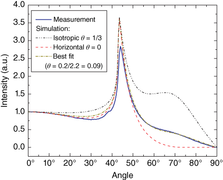
Figure 6.6 Determination of the orientation parameter of the blue fluorescent emitting system using an OLED stack with ETL thickness of 67 nm but without metallic cathode. The p‐polarized angular‐dependent emission pattern is compared to optical simulations yielding an orientation parameter  , i.e. nearly perfectly horizontal alignment of the transition dipole moments.
Source: Ref. [67]. Reproduced with permission of AIP Publishing LLC.
As discussed briefly in previous sections, the shape of the EQE oscillations with emitter/cathode distance, i.e. the relative heights of the first and the second maximum of the direct emission and the boost in efficiency, if the substrate modes are extracted, is strongly influenced by the RQE as well as the orientation of the transition dipole moments, whereas the charge carrier balance and the radiative exciton fraction are only linear scaling factors that do not change with ETL thickness. Hence, from Figure 6.5
b it is obvious that one (or both) of the mentioned factors influencing the shape of the EQE oscillations was not considered properly. Thus, angular‐dependent p‐polarized PL emission pattern analysis was performed for an OLED without metallic cathode at an ETL thickness of 67 nm to get information about the emitter orientation. Figure 6.6 illustrates the measured angular‐dependent intensity for an emission wavelength of 470 nm normalized to zero degree intensity and optical simulations for isotropic and horizontal alignment of the transition dipole moments. The best fit yields an orientation parameter of ![]() , which is in fact nearly completely horizontal and far away from the initially assumed isotropic emitter orientation.
, which is in fact nearly completely horizontal and far away from the initially assumed isotropic emitter orientation.

Figure 6.7 Efficiency analysis of the measured EQE values with and without macroextractor taking the strong horizontal orientation of the TDVs of the emitting species into account and assuming an unchanged radiative exciton fraction. The fit process (solid red line) yields a radiative quantum efficiency of 70%, much lower compared to the isotropic results. However, the fit for substrate mode emission still cannot describe the measured data in an appropriate way.
Source: Ref. [67]. Reproduced with permission of AIP Publishing LLC.
With this information it is now possible to repeat the analysis of the external quantum efficiency measurements for the OLEDs with varying ETL thickness taking the emitter orientation into account. Figure 6.7 illustrates the simulation of both the direct emission values and the substrate mode extraction, using the obtained orientation parameter and a reduced RQE of ![]() . However, there are still some deviations for the substrate mode emission indicating that something is missing. This could either be a charge balance factor
. However, there are still some deviations for the substrate mode emission indicating that something is missing. This could either be a charge balance factor ![]() smaller than one or a radiative exciton fraction
smaller than one or a radiative exciton fraction ![]() larger than 25%. While the former is very unlikely (and would actually require again a higher
larger than 25%. While the former is very unlikely (and would actually require again a higher ![]() value), an enhancement of
value), an enhancement of ![]() by delayed fluorescence is possible.
by delayed fluorescence is possible.

Figure 6.8 Time‐resolved emission ((a) electroluminescence and (b) photoluminescence) in the microsecond range. Both measurements show a strong delayed fluorescence component. Note that the intensity scale is logarithmic.
Source: Ref. [67]. Reproduced with permission of AIP Publishing LLC.
In order to prove this hypothesis, time‐resolved PL and EL spectroscopy is performed in the microsecond range. The excitation was accomplished by a short laser pulse (337 nm, 0.7 ns) or a rectangular electrical pulse (variable height, 20 ![]() s), respectively. The typical decay time for fluorescent emitting molecules is in the range of nanoseconds, hence, if one is detecting a long‐lived emission response in the microsecond range, this gives strong evidence that a mechanism causing delayed fluorescence is present. Figure 6.8 illustrates the results of these measurements and clearly demonstrates the delayed fluorescence decay in both experiments. Note that the RC time of the used OLED is about 500 ns and thus cannot be responsible for the long‐lived decay in the electrical excitation case. Interestingly, the delayed component is decreasing continuously and finally disappears in the photoluminescent experiment, if the sample is cooled to liquid helium temperature. This gives strong evidence that a thermally activated process is responsible for the delayed emission and therewith TTA can be ruled out.
s), respectively. The typical decay time for fluorescent emitting molecules is in the range of nanoseconds, hence, if one is detecting a long‐lived emission response in the microsecond range, this gives strong evidence that a mechanism causing delayed fluorescence is present. Figure 6.8 illustrates the results of these measurements and clearly demonstrates the delayed fluorescence decay in both experiments. Note that the RC time of the used OLED is about 500 ns and thus cannot be responsible for the long‐lived decay in the electrical excitation case. Interestingly, the delayed component is decreasing continuously and finally disappears in the photoluminescent experiment, if the sample is cooled to liquid helium temperature. This gives strong evidence that a thermally activated process is responsible for the delayed emission and therewith TTA can be ruled out.

Figure 6.9 Time‐resolved emission spectroscopy of the prompt fluorescence of the OLEDs. (a) Exemplary photoluminescence decay for an OLED with 184 nm ETL thickness resulting in an excited‐state lifetime of 3.66 ns. (b) Determination of the radiative quantum efficiency using the prompt emission decay times yielding a radiative quantum efficiency  and an intrinsic fluorescence lifetime
  ns.
ns.
Source: Ref. [67]. Reproduced with permission of AIP Publishing LLC.
To reduce the number of free parameters of the fit procedure for the external quantum efficiency, it is mandatory to obtain direct information about the RQE of the prompt fluorescence decay. Therefore, time‐resolved PL spectroscopy in the nanosecond range was carried out. Figure 6.9 illustrates an exemplary measurement and the analysis of the prompt fluorescence lifetimes for different ETL thicknesses. Fitting theses values with optical simulations – taking the already determined dipole orientation into account – results in a RQE ![]() of 45% only, which is clearly much less than both of the previously obtained values.
of 45% only, which is clearly much less than both of the previously obtained values.

Figure 6.10 Summary of the earlier approaches for fitting the EQE values (black and red line) together with the fit using the radiative exciton fraction  as free fit parameter and a radiative quantum efficiency of 45%. The new simulation (blue line) can describe both measured data sets of the EQE with and without macroextractor in a reasonable way, resulting in an enhanced value of
  .
.
Source: Ref. [67]. Reproduced with permission of AIP Publishing LLC.
Turning back to the efficiency analysis of the measured EQE values, it is now possible to perform optical simulations with ![]() as starting value of the fit process,
as starting value of the fit process, ![]() as fixed input, and the radiative exciton fraction as free variable. Figure 6.10 shows that a consistent description of both contributions, direct and substrate emission, can be obtained with one parameter set, yielding
as fixed input, and the radiative exciton fraction as free variable. Figure 6.10 shows that a consistent description of both contributions, direct and substrate emission, can be obtained with one parameter set, yielding ![]() , which is almost 50% higher than the classical value of 0.25. Note that this is only a lower limit for the radiative exciton fraction, as the charge carrier balance was assumed to be unity for the used device.
, which is almost 50% higher than the classical value of 0.25. Note that this is only a lower limit for the radiative exciton fraction, as the charge carrier balance was assumed to be unity for the used device.
This example clearly demonstrates that even in cases where the EQE of an OLED does not exceed the classical limit of 5% for a fluorescent emitter, delayed fluorescence may contribute significantly to the radiative exciton fraction. Moreover, to disentangle these effects and potential implications of nonisotropic emitter orientation, a comprehensive efficiency analysis using complementary experimental techniques combined with optical simulation is required.
6.4.2 Highly Efficient Thermally Activated Delayed Fluorescence Device
In this section we will investigate an OLED with a blue TADF emitter exceeding the classical efficiency limit of 5% by far. Again, by combining different techniques we will disentangle the contributions of the individual factors to the observed high EQE values [74].
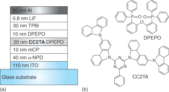
Figure 6.11 (a) OLED stack under investigation. (b) Molecular structure of the emitting system comprising DPEPO (matrix material) and CC2TA (fluorescent dye).
The stack layout of the OLED under investigation together with the molecular structure of the used emitting guest/host system is given in Figure 6.11. From previous investigations, CC2TA (2,4‐bis3‐(9H‐carbazol‐9‐yl)‐9H‐carbazol‐9‐yl‐6‐phenyl‐1,3,5‐triazine) was known to show strong TADF as it exhibits a very small singlet‐to‐triplet energy gap of only 60 meV [22]. The molecular structure follows the donor–acceptor–donor design principle to reduce the exchange splitting of purely organic fluorescent dyes. In this case, two carbazole containing donor groups and one triazine acceptor unit are used. The matrix material DPEPO (bis[2‐(diphenylphosphino)phenyl]ether) is also used as hole blocker, while mCP (1,3‐bis(N‐carbazolyl)benzene) acts as electron blocker. Both of them have high triplet energies so that energy transfer from the triplet state of CC2TA to the surrounding matrix and/or blocker materials is strongly suppressed. For further details we refer to Ref. [22].

Figure 6.12 (a) Current density–voltage characteristics of the OLED depicted in Figure 6.11. The inset shows the sky blue emission spectrum for a current density of 1 mA cm . (b) External quantum efficiency as a function of current density. The maximum EQE of
  % is achieved for 0.01 mA cm
 .
.
Source: Ref. [74]. Reproduced with permission of John Wiley & Sons.
The OLED shows a typical diode behavior with sky blue emission as can be seen in Figure 6.12. The external quantum efficiency of the device reaches a maximum value of ![]() % at 0.01 mA cm
% at 0.01 mA cm![]() , which clearly exceeds the classical limit for fluorescent emitting systems. For higher current densities a moderate roll‐off is observed. In the following, we determine the different contributions to the efficiency including emitter orientation and TADF as independent contributions.
, which clearly exceeds the classical limit for fluorescent emitting systems. For higher current densities a moderate roll‐off is observed. In the following, we determine the different contributions to the efficiency including emitter orientation and TADF as independent contributions.

Figure 6.13 Angular‐dependent PL emission pattern of a thin layer of CC2TA in DPEPO on a glass substrate connected to a half‐cylinder prism. (a) Measured spectra, (b) simulation for isotropic emitter orientation, and (c) simulation for horizontal emitter orientation. All spectra are normalized to zero degree emission.
Source: Ref. [74]. Reproduced with permission of John Wiley & Sons.
Figure 6.13 illustrates the measured angular‐dependent PL emission pattern of a simplified stack, which only consists of a thin emitting layer on a glass substrate attached to a half‐cylinder prism to extract the captured substrate modes, together with the results of optical simulations for isotropic and horizontal orientation of the TDVs. Comparing simulations with measurements clearly shows large deviations for the isotropic case for emission angles higher than 40°, while the horizontal simulation comes quite close to the measured data.

Figure 6.14 Cross section of the angular‐dependent photoluminescence emission pattern for the peak wavelength of 470 nm normalized to zero degree intensity. The dots represent the measurement, while the solid lines show simulations for isotropic (black) and horizontal (red) emitter orientation. The fit (green dashed line) results in an orientation parameter  of 0.08, which means nearly perfect horizontal orientation of the TDVs of the emitting species CC2TA.
Source: Ref. [74]. Reproduced with permission of John Wiley & Sons.
However, in order to determine the orientation parameter for CC2TA in DPEPO, it is useful to analyze the cross section of the angular emission pattern for the peak wavelength of 470 nm. Figure 6.14 shows the results of this investigation. The intensity of the optical simulations as well as of the PL emission is normalized to the zero degree values. The most interesting part of this analysis is the angular range between 40° and 90°, as the emission for extracted substrate modes is located in this region. The fit of the measured data results in an orientation parameter of ![]() , which means, in a simplistic picture, that 92% of the TDVs of the emitting species are aligned parallel to the substrate plane. This horizontal alignment enhances the outcoupling factor and, thus, contributes significantly to the high EQE of the OLEDs.
, which means, in a simplistic picture, that 92% of the TDVs of the emitting species are aligned parallel to the substrate plane. This horizontal alignment enhances the outcoupling factor and, thus, contributes significantly to the high EQE of the OLEDs.

Figure 6.15 Determination of the radiative quantum efficiency of CC2TA in DPEPO via the prompt fluorescence lifetime for a simplified stack design shown as inset. The dots represent the measured decay times for different UGH‐2 thicknesses, acting as optical spacer between the emitting system and a metallic mirror. The red line is the fit using the horizontal emitter orientation while the black dashed line is, for completeness, the corresponding simulation for isotropic distribution of the TDVs. Note that the gray data point was not considered for the fit due to very low intensity in the cavity minimum.
Source: Ref. [74]. Reproduced with permission of John Wiley & Sons.
As next step it is necessary to determine the RQE of the emitting system. Here, we use a simplified stack and not a complete OLED structure with different ETL thicknesses as in the previous section. The layer stack only consists of a glass substrate, a thin layer of the emitting system, the optical spacer UGH‐2 (1,4‐bis(triphenylsilyl)benzene, and a thick silver layer acting as mirror, as depicted in the inset of Figure 6.15. The UGH‐2 layer is implemented as wide bandgap material with high triplet energy to change the distance between the emitting system and the metallic mirror and, thus, to systematically vary the interference conditions for the radiative exciton decay. Figure 6.15 displays the changes of the excited‐state lifetime of the prompt fluorescence emission in the nanosecond range for varying UGH‐2 thickness together with optical simulations for isotropic as well as the present horizontal emitter orientation. Therefore, the behavior for the isotropic transition dipole distribution is only shown for completeness to emphasize the importance of taking emitter orientation into account even for the determination of the RQE of the emitting system. Apparently, the analysis with the correct horizontal orientation of the TDV of the emitting species results in a RQE ![]() of
of ![]() , which is consistent with the PL quantum efficiency of 0.62 measured in an integrating sphere, if the nonisotropic emitter orientation is taken into account. For more information about these calculations, we refer to [74].
, which is consistent with the PL quantum efficiency of 0.62 measured in an integrating sphere, if the nonisotropic emitter orientation is taken into account. For more information about these calculations, we refer to [74].

Figure 6.16 Measured EQE for a thickness optimized device together with optical simulations for a radiative quantum efficiency of 55% and variable ETL (TPBi) thickness. The black line represents a classical simulation with isotropic emitter orientation and a radiative exciton fraction of 25% (without TADF). The blue line corresponds to an enhanced outcoupling factor induced by the horizontal alignment of the TDVs. The red curve illustrates the optical simulation for horizontal emitter orientation and an enhanced radiative exciton fraction of 56% due to TADF, which is in good agreement with the measured data.
Source: Ref. [74]. Reproduced with permission of John Wiley & Sons.
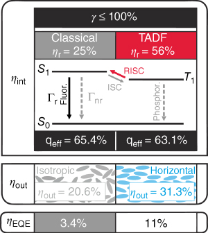
Figure 6.17 Summary of the efficiency analysis for the blue TADF emitter CC2TA in DPEPO. The left column represents a classical fluorescent model with isotropic emitter orientation, while the right column accounts for an enhanced radiative exciton fraction and outcoupling factor due to TADF and horizontal alignment of the TDVs of the emitting species, respectively.
Source: Ref. [74]. Reproduced with permission of John Wiley & Sons.
Finally, it is possible to analyze the measured external quantum efficiency of the thickness optimized device taking all achieved information into account. Figure 6.16 contains three sets of optical simulations for ![]() together with the measured EQE value. It is obvious that the experimental value can only be reproduced, if both the nonisotropic emitter orientation and an enhanced radiative exciton fraction
together with the measured EQE value. It is obvious that the experimental value can only be reproduced, if both the nonisotropic emitter orientation and an enhanced radiative exciton fraction ![]() originating from TADF are considered. Moreover, with the assumption of a charge carrier balance of unity, one can state a lower limit for
originating from TADF are considered. Moreover, with the assumption of a charge carrier balance of unity, one can state a lower limit for ![]() of about 56%.
of about 56%.
For better visualization, Figure 6.17 summarizes the contributions of the individual factors to the measured high EQE value of 11%. It is only possible to properly obtain the internal quantum efficiency, if the correct light‐outcoupling factor (determined by the emitter orientation) is taken. For example, Lee et al. have previously assumed isotropic orientation and, thus, concluded on ![]() (while the true value is only 35.1%). As a consequence, they largely overestimated the radiative exciton fraction as being more than 80% [22].
(while the true value is only 35.1%). As a consequence, they largely overestimated the radiative exciton fraction as being more than 80% [22].
This impressively demonstrates the necessity of a comprehensive efficiency analysis in the case of TADF emitters, which are prone to exhibit nonisotropic orientation distribution of their TDVs in evaporated guest/host systems. For completeness, we note that the nature of the optical transition leading to the observed light emission was not subject of our investigations and also not the orientation of the involved TDV with respect to the molecular frame. However, we want to add that the calculations reported in Ref. [74] were probably oversimplified, as they did not take into account the charge‐transfer character of the optical transitions.
6.4.3 Low Efficiency Roll‐Off Triplet–Triplet Annihilation Device
Apart from TADF, there is a second possibility for an enhanced radiative exciton fraction of fluorescent emitters, namely, TTA. Hence, in this section we will discuss the advantages of this mechanism, in particular, in terms of reduced efficiency roll‐off for high current densities.
We analyzed the well‐known green fluorescent emitter 2,3,6,7‐tetrahydro‐1,1,7,7‐tetramethyl‐1H,5H,11H‐10‐(2‐benzothiazolyl)quinolizino[9,9a,1gh]coumarin (C545T) doped at 1 wt% into the matrix material aluminum‐tris(8‐hydroxyquinoline) (Alq![]() ) [75]. For this emitting system external quantum efficiencies exceeding the classical limit of 5% have already been reported in literature [16, 76]. However, in the analysis of Pu et al. [16], there is a discrepancy of the determined radiative exciton fraction achieved by EQE measurements assuming a standard outcoupling factor of
) [75]. For this emitting system external quantum efficiencies exceeding the classical limit of 5% have already been reported in literature [16, 76]. However, in the analysis of Pu et al. [16], there is a discrepancy of the determined radiative exciton fraction achieved by EQE measurements assuming a standard outcoupling factor of ![]() % and time‐resolved EL investigations, resulting in
% and time‐resolved EL investigations, resulting in ![]() values of 54% and 31%, respectively. This gives strong evidence that the assumption of isotropic emitter orientation may not be valid in this case.
values of 54% and 31%, respectively. This gives strong evidence that the assumption of isotropic emitter orientation may not be valid in this case.

Figure 6.18 (a) Current density–voltage characteristics of a thickness optimized TTA OLED together with the electroluminescence emission spectrum for two different current densities. (b) External quantum efficiency values as a function of the current density. The stack design as well as the chemical structure of C545T is depicted as inset. The measured EQE stays constant over a wide current density region (three orders of magnitude).
Source: Ref. [75]. Reproduced with permission of AIP Publishing LLC.
For this reason, we first fabricated thickness‐optimized devices to reproduce the high external quantum efficiencies exceeding the classical limit of 5%. The current density–voltage characteristics as well as the stack layout, the EL emission spectrum, the chemical structure of C545T, and the EQE for a wide range of current densities are depicted in Figure 6.18. This OLED exhibits a very low onset voltage of only 2 V and shows strong green emission with a peak intensity at 523 nm. The maximum EQE (measured in a calibrated integrating sphere) of roughly 7%, exceeding the classical limit by almost 40%, is reached for a current density of 0.1 mA cm![]() and remains constant until 100 mA cm
and remains constant until 100 mA cm![]() . Thereafter, a fast decrease of the EQE to 1% for a current density of 1000 mA cm
. Thereafter, a fast decrease of the EQE to 1% for a current density of 1000 mA cm![]() is observed. The initial increase of the EQE is caused by unbalanced charge carrier flow for small current densities, while the efficiency roll‐off for high current densities is suggested to be induced by mechanisms such as singlet‐ or triplet‐polaron quenching [47]. Because of the formation of a negative interface polarization due to partial alignment of the permanent dipole moments of the Alq
is observed. The initial increase of the EQE is caused by unbalanced charge carrier flow for small current densities, while the efficiency roll‐off for high current densities is suggested to be induced by mechanisms such as singlet‐ or triplet‐polaron quenching [47]. Because of the formation of a negative interface polarization due to partial alignment of the permanent dipole moments of the Alq![]() molecules and therewith hole accumulation at the CBP/Alq
molecules and therewith hole accumulation at the CBP/Alq![]() interface [77–79], a narrow emission profile located at this position is very likely. Hence, the emitter to cathode distance for this device is given by the sum of the thicknesses of the emitting system and the neat Alq
interface [77–79], a narrow emission profile located at this position is very likely. Hence, the emitter to cathode distance for this device is given by the sum of the thicknesses of the emitting system and the neat Alq![]() layer acting as ETL.
layer acting as ETL.

Figure 6.19 Angular‐dependent photoluminescence cross section for the peak emission intensity at a wavelength of 523 nm for a 15 nm thick film of the emitting system C545T:Alq attached to a half‐cylinder prism. The dots are the measured data points, while the solid lines represent optical simulations for different emitter orientations: isotropic (black) and horizontal (red). The dashed line illustrates the fit resulting in an orientation parameter
  .
.
Source: Ref. [75]. Reproduced with permission of AIP Publishing LLC.
Next, we analyzed the orientation of the transition dipole moments of C545T doped into Alq![]() . Therefore, we used again a simplified stack design with a thin layer (15 nm) of the emitting system on a glass substrate connected to a half‐cylinder prism, and the p‐polarized emission was detected as a function of the emission angle. Figure 6.19 shows the results of this investigation, which yields an orientation parameter
. Therefore, we used again a simplified stack design with a thin layer (15 nm) of the emitting system on a glass substrate connected to a half‐cylinder prism, and the p‐polarized emission was detected as a function of the emission angle. Figure 6.19 shows the results of this investigation, which yields an orientation parameter ![]() of 0.14 indicating a strong horizontal alignment of the TDVs of C545T. Thus, the classical assumption of
of 0.14 indicating a strong horizontal alignment of the TDVs of C545T. Thus, the classical assumption of ![]() % is not valid. Optical simulations reveal that the outcoupling factor of a thickness optimized device as used in this investigation is enhanced by a factor of 1.5 and reaches its maximum of
% is not valid. Optical simulations reveal that the outcoupling factor of a thickness optimized device as used in this investigation is enhanced by a factor of 1.5 and reaches its maximum of ![]() % for an emitter to cathode distance of 65 nm.
% for an emitter to cathode distance of 65 nm.

Figure 6.20 Time‐resolved electroluminescence measurements showing a strong delayed fluorescence component after the electrical pulse. The relative fraction of delayed to prompt fluorescence does not change for different excitation voltages. From the indicated extrapolations (dashed lines), one can calculate the enhancement of the radiative exciton fraction  to be a factor of 1.18.
Source: Ref. [75]. Reproduced with permission of AIP Publishing LLC.
From previous publications it is known that OLEDs with C545T show delayed fluorescence from TTA [14]. Therefore, we performed time‐resolved EL spectroscopy with voltage pulses of variable amplitudes and a length of 50 ![]() s, required to achieve steady‐state conditions, and analyzed the contribution of TTA to the overall EL. Figure 6.20 shows the normalized emission intensities as a function of time for different pulse amplitudes. Note that a reverse bias of
s, required to achieve steady‐state conditions, and analyzed the contribution of TTA to the overall EL. Figure 6.20 shows the normalized emission intensities as a function of time for different pulse amplitudes. Note that a reverse bias of ![]() 4 V was applied to the devices directly after shutting down the forward bias to prevent delayed charge carrier recombination from, e.g. trapped charge carriers, which would also lead to a delayed EL signal. As the device exhibits an RC time of less than 1
4 V was applied to the devices directly after shutting down the forward bias to prevent delayed charge carrier recombination from, e.g. trapped charge carriers, which would also lead to a delayed EL signal. As the device exhibits an RC time of less than 1 ![]() s and the decay time of the delayed fluorescence is much larger than this value, it is possible to determine the contribution of TTA to the total EL by calculating the intersection of the electrical pulse with the extrapolation of the delayed fluorescence signal as depicted in Figure 6.20 by the two dashed lines. The quantitative analysis (for details see Ref. [75]) reveals an enhancement of
s and the decay time of the delayed fluorescence is much larger than this value, it is possible to determine the contribution of TTA to the total EL by calculating the intersection of the electrical pulse with the extrapolation of the delayed fluorescence signal as depicted in Figure 6.20 by the two dashed lines. The quantitative analysis (for details see Ref. [75]) reveals an enhancement of ![]() by a factor of 1.18 yielding an absolute value of 29.5% instead of the classical assumption of 25%. Remarkably, the relative ratios of steady state and delayed components are not affected by variable voltage pulse amplitudes, which means that the contribution of TTA is constant in this range, which in turn is in good agreement with the measured EQE values being more or less constant between 0.1 and 100 mA cm
by a factor of 1.18 yielding an absolute value of 29.5% instead of the classical assumption of 25%. Remarkably, the relative ratios of steady state and delayed components are not affected by variable voltage pulse amplitudes, which means that the contribution of TTA is constant in this range, which in turn is in good agreement with the measured EQE values being more or less constant between 0.1 and 100 mA cm![]() .
.

Figure 6.21 Measured EQE values for two OLEDs exhibiting different ETL thicknesses (dots) together with optical simulations for different assumptions for the radiative exciton fraction and emitter orientation. The comparison results in a radiative exciton fraction  of 28.4% that is in good agreement with the value obtained from time‐resolved electroluminescence investigations.
Source: Ref. [75]. Reproduced with permission of AIP Publishing LLC.
In order to complete the efficiency analysis for the presented OLED type, we finally compare the measured EQE values for two OLEDs with different emitter to cathode distances (ETL thicknesses) with optical simulation for variable assumptions for the radiative exciton fraction and emitter orientation. We used a RQE for the emitting system derived from its PL quantum efficiency of ![]() [80], and the charge carrier balance of the device was set to unity to obtain a lower limit for
[80], and the charge carrier balance of the device was set to unity to obtain a lower limit for ![]() . Figure 6.21 illustrates the measured EQE values for both OLEDs together with three different optical simulations. It can clearly be seen that the high external quantum efficiencies can only be reproduced by the optical simulation using the determined horizontal emitter orientation and an enhanced radiative exciton fraction
. Figure 6.21 illustrates the measured EQE values for both OLEDs together with three different optical simulations. It can clearly be seen that the high external quantum efficiencies can only be reproduced by the optical simulation using the determined horizontal emitter orientation and an enhanced radiative exciton fraction ![]() of 28.4%, which is in good agreement with the value obtained from the time‐resolved EL measurements presented before. Thus, the importance of taking nonisotropic emitter orientation into account is again clearly demonstrated, because otherwise
of 28.4%, which is in good agreement with the value obtained from the time‐resolved EL measurements presented before. Thus, the importance of taking nonisotropic emitter orientation into account is again clearly demonstrated, because otherwise ![]() would be strongly overestimated.
would be strongly overestimated.
In total, the main boost in efficiency originates from the horizontal alignment of the transition dipole moments of the emissive species (40% relative enhancement), and the increase in the radiative exciton fraction induced by TTA only plays a minor role (14% relative enhancement).
6.5 Conclusion
More than 15 years after the first presentation of second‐generation emitter materials based on phosphorescent metal–organic complexes, a third generation of emitter materials deploying triplet harvesting by delayed fluorescence is gaining more and more interest. OLEDs with extraordinary external quantum efficiency – comparable to their phosphorescent counterparts – clearly corroborate the huge potential of this family of materials.
In this chapter we presented an approach for a comprehensive efficiency analysis of OLEDs incorporating these third‐generation emitting systems. In contrast to phosphorescent devices, for which two of the four factors determining the external quantum efficiency are known (the charge carrier balance and the radiative exciton fraction are unity for these OLEDs), one has to determine three factors independently from each other for delayed fluorescence OLEDs as the radiative exciton fraction becomes a free parameter. Furthermore, since the chemical structure of this new emitter class is based on the donor–acceptor principle, the geometrical shape of these molecules promotes nonisotropic orientation of their transition dipole moments when evaporated from the gas phase. Hence, this effect has to be taken carefully into account in a comprehensive efficiency analysis. If the anisotropy of the TDVs distribution is ignored, the radiative exciton fraction is clearly overestimated.
In the presented case studies, all investigated third‐generation emitting materials exhibit strong horizontal emitter orientation enhancing the light‐outcoupling factor by almost 50% resulting in a huge boost of the external quantum efficiency of devices using these emitting systems. This clearly demonstrates, on the one hand, the importance of taking nonisotropic emitter orientation properly into account for the efficiency analysis, i.e. for determining the increased radiative exciton fraction due to TADF or TTA, as well as, on the other hand, the room for further improvement of such devices as the radiative exciton fraction is still not at its limits in the considered devices. If efficient triplet harvesting and high radiative efficiency can be combined with horizontal orientation of the TDVs of these molecules, these third‐generation emitting materials have the potential to match their phosphorescent counterparts as, for the moment, these molecules only exhibit moderate horizontal emitter orientation. Nevertheless, these third‐generation emitter materials also need to be further improved to reach stability levels of phosphorescent emitters [81–83].
Acknowledgments
The authors thank the German Ministry of Education and Research (BMBF, contract No. 13N12240), Deutsche Forschungsgemeinschaft (DFG, contract No. BR 1728/13‐1), and Bayerische Forschungsstiftung for funding. Furthermore, we acknowledge support by the Japanese Society for the Promotion of Science (JSPS) within their Summer Programs. We are grateful to OSRAM OLED GmbH (Regensburg, Germany) and the research group of Prof. Chihaya Adachi (Kyushu University, Fukuoka, Japan) for providing samples and fruitful discussions. Moreover, we acknowledge the contributions of Christian Mayr, Thomas Lampe, Bert J. Scholz and Jörg Frischeisen (University of Augsburg, Germany), Daniel S. Setz, Andreas F. Rausch, Thomas Wehlus and Thilo C. G. Reusch (Osram OLED GmbH, Germany), Michael Flämmich, Dirk Michaelis and Norbert Danz (Fraunhofer IOF, Germany), and Sae Youn Lee, Takuma Yasuda, and Chihaya Adachi (Kyushu University, Japan) to part of the results presented in this chapter.
References
- 1 Pope, M., Kallmann, H.P., and Magnante, P. (1963). Electroluminescence in organic crystals. J. Chem. Phys. 38 (8): 2042–2043.
- 2 Tang, C.W. and VanSlyke, S.A. (1987). Organic electroluminescent diodes. Appl. Phys. Lett. 51 (12): 913–915.
- 3 Burroughes, J.H., Bradley, D.D.C., Brown, A.R., Marks, R.N., Mackay, K., Friend, R.H., Burns, P.L., and Holmes, A.B. (1990). Light‐emitting diodes based on conjugated polymers. Nature 347 (6293): 539–541.
- 4 Tsutsui, T., Aminaka, E., Lin, C.P., and Kim, D.U. (1997). Extended molecular design concept of molecular materials for electroluminescence: sublimed‐dye films, molecularly doped polymers and polymers with chromophores. Philos. Trans. R. Soc. London, Ser. A 355 (1725): 801–814.
- 5 Baldo, M.A., O'Brien, D.F., You, Y., Shoustikov, A., Sibley, S., Thompson, M.E., and Forrest, S.R. (1998). Highly efficient phosphorescent emission from organic electroluminescent devices. Nature 395 (6698): 151–154.
- 6 Yersin, H. ed. (2007). Highly Efficient OLEDs with Phosphorescent Materials. Wiley‐VCH.
- 7 Brutting, W. and Adachi, C. ed. (2012). Physics of Organic Semiconductors. Wiley‐VCH.
- 8 Mullen, K. and Scherf, U. ed. (2005). Organic Light Emitting Devices. Wiley‐VCH.
- 9 Yook, K.S. and Lee, J.Y. (2012). Organic materials for deep blue phosphorescent organic light‐emitting diodes. Adv. Mater. 24 (24): 3169–3190.
- 10 Lee, J., Chen, H.‐F., Batagoda, T., Coburn, C., Djurovich, P.I., Thompson, M.E., and Forrest, S.R. (2016). Deep blue phosphorescent organic light‐emitting diodes with very high brightness and efficiency. Nat. Mater. 15 (1): 92–98.
- 11 Uoyama, H., Goushi, K., Shizu, K., Nomura, H., and Adachi, C. (2012). Highly efficient organic light‐emitting diodes from delayed fluorescence. Nature 492: 234–238.
- 12 Kondakov, D.Y. (2007). Characterization of triplet–triplet annihilation in organic light‐emitting diodes based on anthracene derivatives. J. Appl. Phys. 102 (11): 114504.
- 13 Kondakov, D.Y., Pawlik, T.D., Hatwar, T.K., and Spindler, J.P. (2009). Triplet annihilation exceeding spin statistical limit in highly efficient fluorescent organic light‐emitting diodes. J. Appl. Phys. 106 (12): 124510.
- 14 Luo, Y. and Aziz, H. (2010). Correlation between triplet–triplet annihilation and electroluminescence efficiency in doped fluorescent organic light‐emitting devices. Adv. Funct. Mater. 20 (8): 1285–1293.
- 15 Yokoyama, D., Park, Y., Kim, B., Kim, S., Pu, Y.‐J., Kido, J., and Park, J. (2011). Dual efficiency enhancement by delayed fluorescence and dipole orientation in high‐efficiency fluorescent organic light‐emitting diodes. Appl. Phys. Lett. 99 (12): 123303.
- 16 Pu, Y.‐J., Nakata, G., Satoh, F., Sasabe, H., Yokoyama, D., and Kido, J. (2012). Optimizing the charge balance of fluorescent organic light‐emitting devices to achieve high external quantum efficiency beyond the conventional upper limit. Adv. Mater. 24 (13): 1765–1770.
- 17 Suzuki, T., Nonaka, Y., Watabe, T., Suzuki, T., Nonaka, Y., Watabe, T., Nakashima, H., Seo, S., Shitagaki, S., and Yamazaki, S. (2014). Highly efficient long‐life blue fluorescent organic light‐emitting diode exhibiting triplet‐triplet annihilation effects enhanced by a novel hole‐transporting material. Jpn. J. Appl. Phys. 53: 052102.
- 18 Chiang, C.‐J., Kimyonok, A., Etherington, M.K., Griffiths, G.C., Jankus, V., Turksoy, F., and Monkman, A.P. (2013). Ultrahigh efficiency fluorescent single and bi‐layer organic light emitting diodes: the key role of triplet fusion. Adv. Funct. Mater. 23 (6): 739–746.
- 19 Endo, A., Ogasawara, M., Takahashi, A., Yokoyama, D., Kato, Y., and Adachi, C. (2009). Thermally activated delayed fluorescence from sn–porphyrin complexes and their application to organic light emitting diodes – a novel mechanism for electroluminescence. Adv. Mater. 21 (47): 4802–4806.
- 20 Endo, A., Sato, K., Yoshimura, K., Kai, T., Kawada, A., Miyazaki, H., and Adachi, C. (2011). Efficient up‐conversion of triplet excitons into a singlet state and its application for organic light emitting diodes. Appl. Phys. Lett. 98 (8): 083302.
- 21 Czerwieniec, R., Yu, J., and Yersin, H. (2011). Blue‐light emission of Cu(I) complexes and singlet harvesting. Inorg. Chem. 50 (17): 8293–8301.
- 22 Lee, S.Y., Yasuda, T., Nomura, H., and Adachi, C. (2012). High‐efficiency organic light‐emitting diodes utilizing thermally activated delayed fluorescence from triazine‐based donor–acceptor hybrid molecules. Appl. Phys. Lett. 101 (9): 093306.
- 23 Zhang, Q., Li, B., Huang, S., Nomura, H., Tanaka, H., and Adachi, C. (2014). Efficient blue organic light‐emitting diodes employing thermally activated delayed fluorescence. Nature 8: 326–332.
- 24 Dias, F.B., Bourdakos, K.N., Jankus, V., Moss, K.C., Kamtekar, K.T., Bhalla, V., Santos, J., Bryce, M.R., and Monkman, A.P. (2013). Triplet harvesting with 100% efficiency by way of thermally activated delayed fluorescence in charge transfer OLED emitters. Adv. Mater. 25 (27): 3707–3714.
- 25 Jankus, V., Data, P., Graves, D., McGuinness, C., Santos, J., Bryce, M.R., Dias, F.B., and Monkman, A.P. (2014). Highly efficient TADF OLEDs: how the emitter–host interaction controls both the excited state species and electrical properties of the devices to achieve near 100% triplet harvesting and high efficiency. Adv. Funct. Mater. 24 (39): 6178–6186.
- 26 Nobuyasu, R.S., Ren, Z., Griffiths, G.C., Batsanov, A.S., Data, P., Yan, S., Monkman, A.P., Bryce, M.R., and Dias, F.B. (2016). Rational design of TADF polymers using a donor–acceptor monomer with enhanced TADF efficiency induced by the energy alignment of charge transfer and local triplet excited states. Adv. Opt. Mater. 4 (5): 653.
- 27 Parker, C.A. (1963). Sensitized p‐type delayed fluorescence. Proc. R. Soc. London, Ser. A 276 (1364): 125–135.
- 28 Jankus, V., Chiang, C.‐J., Dias, F., and Monkman, A.P. (2013). Deep blue exciplex organic light‐emitting diodes with enhanced efficiency; P‐type or E‐type triplet conversion to singlet excitons? Adv. Mater. 25 (10): 1455–1459.
- 29 Cho, Y.J., Yook, K.S., and Lee, J.Y. (2014). A universal host material for high external quantum efficiency close to 25% and long lifetime in green fluorescent and phosphorescent OLEDs. Adv. Mater. 26 (24): 4050–4055.
- 30 Kim, B.S. and Lee, J.Y. (2014). Engineering of mixed host for high external quantum efficiency above 25% in green thermally activated delayed fluorescence device. Adv. Funct. Mater. 24 (25): 3970–3977.
- 31 Sun, J.W., Lee, J.‐H., Moon, C.‐K., Kim, K.‐H., Shin, H., and Kim, J.‐J. (2014). A fluorescent organic light‐emitting diode with 30% external quantum efficiency. Adv. Mater. 26: 5684–5688.
- 32 Kaji, H., Suzuki, H., Fukushima, T., Shizu, K.I., Suzuki, K., Kubo, S., Komino, T., Oiwa, H., Suzuki, F., Wakamiya, A., Murata, Y., and Adachi, C. (2015). Purely organic electroluminescent material realizing 100% conversion from electricity to light. Nat. Commun. 6: 8476.
- 33 Frischeisen, J., Yokoyama, D., Endo, A., Adachi, C., and Brütting, W. (2011). Increased light outcoupling efficiency in dye‐doped small molecule organic light‐emitting diodes with horizontally oriented emitters. Org. Electron. 12 (5): 809–817.
- 34 Kohler, A. and Bassler, H. ed. (2015). Electronic Processes in Organic Semiconductors. Wiley‐VCH.
- 35 Schwoerer, M. and Wolf, H.C. ed. (2006). Organic Molecular Solids. Wiley‐VCH.
- 36 Lüssem, B., Riede, M., and Leo, K. (2013). Doping of organic semiconductors. Phys. Status Solidi A 210 (1): 9–43.
- 37 Pfeiffer, M., Leo, K., Zhou, X., Huang, J.S., Hofmann, M., Werner, A., and Blochwitz-Nimoth, J. (2003). Doped organic semiconductors: physics and application in light emitting diodes. Org. Electron. 4 (2): 89–103.
- 38 Adachi, C., Baldo, M.A., Thompson, M.E., and Forrest, S.R. (2001). Nearly 100% internal phosphorescence efficiency in an organic light‐emitting device. J. Appl. Phys. 90 (10): 5048–5051.
- 39 Purcell, E.M. (1946). Spontaneous emission probabilities at radio frequencies. Phys. Rev. 69: 681.
- 40 Barnes, W.L. (1998). Fluorescence near interfaces: the role of photonic mode density. J. Mod. Opt. 45 (4): 661–699.
- 41 Neyts, K.A. (1998). Simulation of light emission from thin‐film microcavities. J. Opt. Soc. Am. A 15 (4): 962–971.
- 42 Furno, M., Meerheim, R., Hofmann, S., Lüssem, B., and Leo, K. (2012). Efficiency and rate of spontaneous emission in organic electroluminescent devices. Phys. Rev. B 85: 115205.
- 43 Brütting, W., Frischeisen, J., Schmidt, T.D., Scholz, B.J., and Mayr, C. (2012). Device efficiency of organic light‐emitting diodes: progress by improved light outcoupling. Phys. Status Solidi A 210: 44–65.
- 44 Setz, D.S., Schmidt, T.D., Flämmich, M., Nowy, S., Frischeisen, J., Krummacher, B.C., Dobbertin, T., Heuser, K., Michaelis, D., Danz, N., Brütting, W., and Winnacker, A. (2011). Comprehensive efficiency analysis of organic light‐emitting devices. J. Photonics Energy 1 (1): 011006.
- 45 Murawski, C., Leo, K., and Gather, M.C. (2013). Efficiency roll‐off in organic light‐emitting diodes. Adv. Mater. 25 (47): 6801–6827.
- 46 Wehrmeister, S., Jäger, L., Wehlus, T., Rausch, A.F., Reusch, T.C.G., Schmidt, T.D., and Brütting, W. (2015). Combined electrical and optical analysis of the efficiency roll‐off in phosphorescent organic light‐emitting diodes. Phys. Rev. Appl. 3: 024008.
- 47 Zhang, Y. and Forrest, S.R. (2012). Triplets contribute to both an increase and loss in fluorescent yield in organic light emitting diodes. Phys. Rev. Lett. 108: 267404.
- 48 Gather, M.C. and Reineke, S. (2015). Recent advances in light outcoupling from white organic light‐emitting diodes. J. Photonics Energy 5 (1): 057607.
- 49 Baldo, M.A., Lamansky, S., Burrows, P.E., Thompson, M.E., and Forrest, S.R. (1999). Very high‐efficiency green organic light‐emitting devices based on electrophosphorescence. Appl. Phys. Lett. 75 (1): 4–6.
- 50 Baldo, M.A., O'Brien, D.F., Thompson, M.E., and Forrest, S.R. (1999). Excitonic singlet‐triplet ratio in a semiconducting organic thin film. Phys. Rev. B 60 (20): 14422–14428.
- 51 Wohlgenannt, M., Tandon, K., Mazumdar, S., Ramasesha, S., and Vardeny, Z.V. (2001). Formation cross‐sections of singlet and triplet excitons in [pi]‐conjugated polymers. Nature 409 (6819): 494–497.
- 52 Barford, W., Bursill, R.J., and Makhov, D.V. (2010). Spin‐orbit interactions between interchain excitations in conjugated polymers. Phys. Rev. B 81: 035206.
- 53 Pope, M. and Swenberg, C.E. ed. (1999). Electronic Processes in Organic Crystals and Polymers. Oxford University Press.
- 54 Köhler, A. and Bässler, H. (2009). Triplet states in organic semiconductors. Mater. Sci. Eng., R 66 (4–6): 71–109.
- 55 van Eersel, H., Bobbert, P.A., Janssen, R.A.J., and Coehoorn, R. (2014). Monte Carlo study of efficiency roll‐off of phosphorescent organic light‐emitting diodes: evidence for dominant role of triplet‐polaron quenching. Appl. Phys. Lett. 105 (14): 143303.
- 56 Coehoorn, R., van Eersel, H., Bobbert, P., and Janssen, R. (2015). Kinetic Monte Carlo study of the sensitivity of OLED efficiency and lifetime to materials parameters. Adv. Funct. Mater. 25: 2024–2037.
- 57 Yokoyama, D. (2011). Molecular orientation in small‐molecule organic light‐emitting diodes. J. Mater. Chem. 21: 19187–19202.
- 58 Flämmich, M., Frischeisen, J., Setz, D.S., Michaelis, D., Krummacher, B.C., Schmidt, T.D., Brütting, W., and Danz, N. (2011). Oriented phosphorescent emitters boost OLED efficiency. Org. Electron. 12 (10): 1663–1668.
- 59 Schmidt, T.D., Scholz, B.J., Mayr, C., and Brütting, W. (2013). Efficiency analysis of organic light‐emitting diodes based on optical simulations. IEEE J. Sel. Top. Quantum Electron. 19 (5): 1–12.
- 60 Kim, S.‐Y., Jeong, W.‐I., Mayr, C., Park, Y.‐S., Kim, K.‐H., Lee, J.‐H., Moon, C.‐K., Brütting, W., and Kim, J.‐J. (2013). Organic light‐emitting diodes with 30% external quantum efficiency based on a horizontally oriented emitter. Adv. Funct. Mater. 23 (31): 3896–3900.
- 61 Callens, M.K., Yokoyama, D., and Neyts, K. (2015). Anisotropic materials in OLEDs for high outcoupling efficiency. Opt. Express 23 (16): 21128–21148.
- 62 Qu, Y., Slootsky, M., and Forrest, S.R. (2015). Enhanced light extraction from organic light‐emitting devices using a sub‐anode grid. Nat. Photonics 9: 758–763.
- 63 Schmidt, T.D., Setz, D.S., Flämmich, M., Frischeisen, J., Michaelis, D., Krummacher, B.C., Danz, N., and Brütting, W. (2011). Evidence for non‐isotropic emitter orientation in a red phosphorescent organic light‐emitting diode and its implications for determining the emitter's radiative quantum efficiency. Appl. Phys. Lett. 99 (16): 163302.
- 64 Jurow, M.J., Mayr, C., Schmidt, T.D., Lampe, T., Djurovich, P.I., Brütting, W., and Thompson, M.E. (2016). Understanding and predicting the orientation of heteroleptic phosphors in organic light‐emitting materials. Nat. Mater. 15: 85–91.
- 65 Chen, X.‐W., Choy, W.C.H., Liang, C.J., Wai, P.K.A., and He, S. (2007). Modifications of the exciton lifetime and internal quantum efficiency for organic light‐emitting devices with a weak/strong microcavity. Appl. Phys. Lett. 91 (22): 221112.
- 66 Nowy, S., Krummacher, B.C., Frischeisen, J., Reinke, N.A., and Brütting, W. (2008). Light extraction and optical loss mechanisms in organic light‐emitting diodes: influence of the emitter quantum efficiency. J. Appl. Phys. 104 (12): 123109.
- 67 Schmidt, T.D., Setz, D.S., Flämmich, M., Frischeisen, J., Michaelis, D., Mayr, C., Rausch, A.F, Wehlus, T., Scholz, B.J., Reusch, T.C.G., Danz, N., and Brütting, W. (2013). Comprehensive efficiency analysis of organic light‐emitting diodes featuring emitter orientation and triplet‐to‐singlet up‐conversion. Appl. Phys. Lett. 103 (9): 093303.
- 68 Giebink, N.C. and Forrest, S.R. (2008). Quantum efficiency roll‐off at high brightness in fluorescent and phosphorescent organic light emitting diodes. Phys. Rev. B 77 (23): 235215.
- 69 Schmidt, T.D., Flämmich, M., Scholz, B.J., Michaelis, D., Mayr, C., Danz, N., and Brütting, W. (2012). Non‐isotropic emitter orientation and its implications for efficiency analysis of organic light‐emitting diodes. Proceedings of SPIE, Volume 8435, p. 843513.
- 70 Frischeisen, J., Yokoyama, D., Adachi, C., and Brütting, W. (2010). Determination of molecular dipole orientation in doped fluorescent organic thin films by photoluminescence measurements. Appl. Phys. Lett. 96 (7): 073302.
- 71 Flämmich, M., Gather, M.C., Danz, N., Michaelis, D., Bräuer, A.H., Meerholz, K., and Tünnermann, A. (2010). Orientation of emissive dipoles in OLEDs: quantitative in situ analysis. Org. Electron. 11 (6): 1039–1046.
- 72 Meerheim, R., Furno, M., Hofmann, S., Lüssem, B., and Leo, K. (2010). Quantification of energy loss mechanisms in organic light‐emitting diodes. Appl. Phys. Lett. 97 (25): 253305.
- 73 Schmidt, T.D., Reichardt, L.J., Rausch, A.F., Wehrmeister, S., Scholz, B.J., Mayr, C., Wehlus, T., Ciarnain, R.M., Danz, N., Reusch, T.C.G., and Brütting, W. (2014). Extracting the emitter orientation in organic light‐emitting diodes from external quantum efficiency measurements. Appl. Phys. Lett. 105 (4): 043302.
- 74 Mayr, C., Lee, S.Y., Schmidt, T.D., Yasuda, T., Adachi, C., and Brütting, W. (2014). Efficiency enhancement of organic light‐emitting diodes incorporating a highly oriented thermally activated delayed fluorescence emitter. Adv. Funct. Mater. 24 (33): 5232–5239.
- 75 Mayr, C., Schmidt, T.D., and Brütting, W. (2014). High‐efficiency fluorescent organic light‐emitting diodes enabled by triplet–triplet annihilation and horizontal emitter orientation. Appl. Phys. Lett. 105 (18): 183304.
- 76 Okumoto, K., Kanno, H., Hamaa, Y., Takahashi, H., and Shibata, K. (2006). Green fluorescent organic light‐emitting device with external quantum efficiency of nearly 10%. Appl. Phys. Lett. 89 (6): 063504.
- 77 Schmidt, T.D., Setz, D.S., Flämmich, M., Scholz, B.J., Jaeger, A., Diez, C., Michaelis, D., Danz, N., and Brütting, W. (2012). Degradation induced decrease of the radiative quantum efficiency in organic light‐emitting diodes. Appl. Phys. Lett. 101 (10): 103301.
- 78 Noguchi, Y., Miyazaki, Y., Tanaka, Y., Sato, N., Nakayama, Y., Schmidt, T.D., Brütting, W., and Ishii, H. (2012). Charge accumulation at organic semiconductor interfaces due to a permanent dipole moment and its orientational order in bilayer devices. J. Appl. Phys. 111: 114508.
- 79 Nowy, S., Ren, W., Elschner, A., Lövenich, W., and Brütting, W. (2010). Impedance spectroscopy as a probe for the degradation of organic light‐emitting diodes. J. Appl. Phys. 107 (5): 054501.
- 80 Tian, M., Luo, J., and Liu, X. (2009). Highly efficient organic light‐emitting devices beyond theoretical prediction under high current density. Opt. Express 17 (24): 21370–21375.
- 81 Noguchi, Y., Kim, H.‐J., Ishino, R., Goushi, K., Adachi, C., Nakayama, Y., and Ishii, H. (2015). Charge carrier dynamics and degradation phenomena in organic light‐emitting diodes doped by a thermally activated delayed fluorescence emitter. Org. Electron. 17 (0): 184–191.
- 82 Sandanayaka, A.S.D., Matsushima, T., and Adachi, C. (2015). Degradation mechanisms of organic light‐emitting diodes based on thermally activated delayed fluorescence molecules. J. Phys. Chem. C 119 (42): 23845–23851.
- 83 Nakanotani, H., Masui, K., Nishide, J., Shibata, T., and Adachi, C. (2013). Promising operational stability of high‐efficiency organic light‐emitting diodes based on thermally activated delayed fluorescence. Sci. Rep. 3: 2127.