
15
Status and Next Steps of TADF Technology: An Industrial Perspective
Alhama Arjona‐Esteban1 and Daniel Volz2
1cynora GmbH, Werner-von-Siemens-Straße 2-6, Gebäude 5110, 76646 Bruchsal, Germany
2McKinsey & Company, Inc., Taunustor 1, 60310 Frankfurt, Germany
The scope of this chapter is a discussion of the thermally activated delayed fluorescence (TADF) technology from an industrial point of view, focusing on potential motivating factors favoring the use of TADF in commercial products, as well as current roadblocks.
In the last few years, the development of new materials has had a significant impact on the industrial application of organic light‐emitting diodes (OLEDs). Thanks to new functional materials, OLED displays with superior performance are now being used in smart watches, smartphones, and TVs. However, there is still room for improvement in areas like display resolution and energy efficiency.
With TADF, a new concept has been established to tackle these issues and will – once again through new, advanced materials – lead to superior products.
This chapter is divided in four sections. First, the key arguments for the use of TADF materials from the market's perspective will be discussed. Second, a status update for blue TADF technology as of the beginning of the year 2017 is presented. Third, we point out new trends concerning the use of TADF materials as hosts and finally conclude this chapter with an outlook.
15.1 What Does the Market Want?
Despite their first development in the late 1980s [1], OLEDs began their rise in commercial products only some years ago. These flat and flexible large‐area light sources offer unique benefits compared with other electroluminescent devices such as color tunability, very fast switching timer, easy processing of the devices, and no need of color filters (even though LCD technology and OLED technology may be fused). The materials are nontoxic and in principle can be sustainable [2], offering the possibility to address mass markets.
Many applications are imaginable for OLED technology, ranging from printed light sources to flexible displays. While people dream of realizing printed OLEDs, which was proven to be possible on lab scale, OLEDs made their commercial debut in vacuum‐processed, high‐performance displays that were employed in smartphones and smart watches, manufactured by companies such as Samsung or LG in Korea.
Unlike LEDs, OLEDs consist of several very thin stacked layers [3, 4]. Because of their form factor, they can serve as two‐dimensional light sources, thus enabling new applications: Recently realized smartphones demonstrated bendable displays using OLED technology. Furthermore, product designers dream of incorporating luminescent foils made from OLEDs into the design of consumer packaging as “smart labels,” on semitransparent light‐emitting windows and even on the front of buildings as decorative elements. While it is still early to predict if we will ever see such products, it is likely that the use of OLED technology for high‐end and potentially mass‐produced low‐cost applications will drastically increase.
15.1.1 The Emitter Materials: Heart of the OLED
Herein, we will focus on the emitting materials (see Table 15.1 and Figure 15.1), which are responsible for transforming excitons into visible light. The excitons formed in the device by recombination of positive and negative charge carriers are divided into singlet (25%) and triplet (75%) excitons due to spin statistics. In order to fabricate efficient OLEDs, emitter molecules that are able to transform both kinds of excitons into light are preferred.
Table 15.1 Main difference between the main emission mechanisms used in OLEDs.
| Performance | Key feature | |
| FLUO | 25% of the energy can be used for light generation | Focus on efficient emission from the S1 to S0 level to use singlet exciton emission. Generally being used for blue and often green pixels |
| PHOS | 100% of the energy can be used for light generation |
Heavy‐metal‐based materials that feature large spin–orbit coupling to harvest both singlet and triplet excitons. Metals can be iridium, platinum, or osmium, for example. Generally used for red pixels and in some cases also in green pixels. Blue PHOS emitters do not show enough stability |
| TADF | 100% of the energy can be used for light generation |
Comparable efficiencies to PHOS but a higher stability is expected Materials feature carefully adjusted energy levels, S1 and T1, to allow for a small ΔE(S–T) to harvest both singlet and triplet excitons |

Figure 15.1 Exciton statistics in OLEDs and their emissive decay paths. Fluorescence (FLUO) often relates to the first emitter material generation. Phosphorescence (PHOS) is the second material generation. TADF marks the latest conceptual development.
Source: Figure courtesy of CYNORA.
Looking at the emitter materials in more detail, three main radiative decay mechanisms are used to transform electrical energy into light: fluorescence (FLUO), phosphorescence (PHOS), and TADF. In the first OLEDs, fluorescent materials were used [5]. Around 1998, it was found that phosphorescent materials could also be applied in OLEDs, which led to a drastic increase in efficiency [6, 7]. Recently, emitters based on TADF were also shown to be suitable for very efficient OLED devices [8–12]. For a more detailed description of the technical background of TADF, we refer the reader to the other chapters in this book.
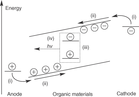
Figure 15.2 Elemental processes during the operation of an OLED. Basic steps are (i) injection of charge carriers in the organic materials, (ii) transport of the charge carriers, which is driven by Coulomb attraction, (iii) formation of excitons, and (iv) emission of light. In this complex system, the emitter (dashed line) has to match all other layers to function in an efficient manner.
Source: Ref. [2]. Reproduced with permission of Royal Society of Chemistry.
A potential TADF emitter material for industrial OLED applications has to satisfy several criteria:
- Performance: OLEDs are ultimately manufactured as display components in devices such as TVs and smartphones; further applications are lighting units for general lighting application and for the automotive industry (taillights). For both fields, the key performance indicators, device efficiency, color point of the device, and its operational stability, are critical. While the assessment of a material's potential is possible based on photoluminescence quantum efficiency (PLQY), a high PLQY is ultimately irrelevant when the proven performance in a device is lower and cannot be raised.
- Compatibility: Apart from providing the expected performance, a TADF material also needs to be compatible with the basic OLED layout. If the reduction or oxidation potential is far away from the other materials, it cannot be implemented in a working OLED architecture (compare with Figure 15.2). The energy levels (highest occupied molecular orbital (HOMO) and lowest unoccupied molecular orbital (LUMO) energy) have to match the other materials in the OLED stack in order to facilitate barrier‐free charge transport, a low operating voltage, high brightness, and good stability. Another compatibility aspect, which is discussed in Section , is processing. At this point, vacuum processing still dominates industrial OLED manufacturing, meaning that nonsublimable compounds are likely not to be suitable for implementation in a commercial product in the foreseeable future.
- Availability. To be implemented in a commercial product, TADF materials need to be available in a sufficient amount. This is somewhat connected to the number of synthetic steps and the complexity of the molecular structure, but there are no fixed guidelines since (looking at many commercial specialty chemicals and pharmaceuticals) optimization of synthetic procedures often opens straightforward routes to seemingly incredible complex structures, while relatively simple‐looking structures need to be sorted out because they cannot be made in large quantities. Availability can also encompass considerations of intellectual property and having a so‐called freedom to operate (FTO), which goes beyond the scope of this chapter [13]. What is partly connected to availability of a material is its sustainability, an aspect we previously discussed in detail [2] and will also be covered in Section 1.3.
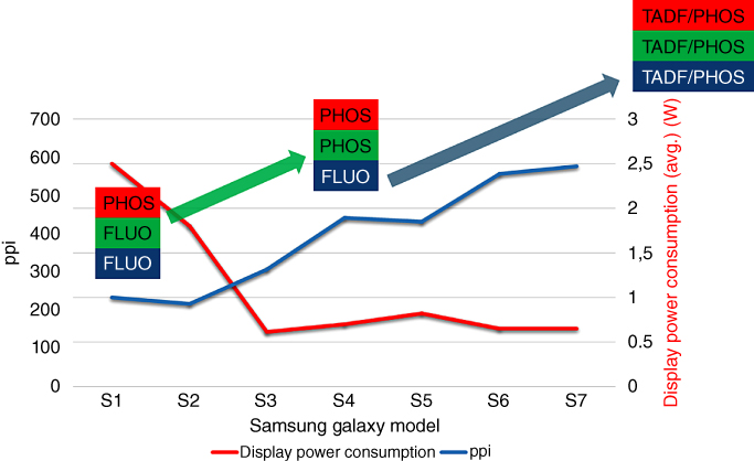
Figure 15.3 The display resolution (in pixel per inch (ppi)) and average power consumption (in W) of several generation of the Samsung Galaxy smartphone, which features OLED displays. Significant improvement was connected to the use of new material generations. In the future, all three colors may be generated by phosphorescent or TADF emitters.
Source: Figure courtesy of CYNORA.
The drastic impact of using different emitter materials on commercial products can be seen in Figure 15.3, where selected key performance indicators are plotted for various generations of Samsung Galaxy smartphones. The initial commercialization of OLED displays was possible only after the development of phosphorescent red emitters with suitable stability and efficiency [6]. Consequently, the first generation, the S1, featured fluorescent materials for green and blue pixels, while red pixels contained phosphorescent materials. After the introduction of green phosphorescent materials, the average power consumption significantly dropped from 2.5 to well below 1 W. On the other hand, the display's resolution was doubled to roughly 400 pixels per inch. Using the more efficient phosphorescent green materials allowed the display manufacturers to significantly decrease the size of green pixels, which allowed for an increase of the resolution and an improved customer experience.
15.1.2 Processing Aspects
The large majority of the OLED products available on the market are based on small molecules deposited via physical vapor deposition. The current deposition technique of choice for industrial OLED production is vacuum thermal evaporation (VTE). The organic molecules or metals are heated in a vacuum chamber with pressures below 5 × 10⁻⁵ mbar; they evaporate and then condense on a cooled substrate. The temperature needed for sublimation is most typically up to 300 °C for organics and between 500 and 1000 °C for metals. The patterning of the layers is generally done with a shadow mask.
These techniques allow for the fabrication of multilayer OLEDs with a good control of the layer thicknesses [3]. It is also convenient to employ vacuum equipment that is already used in the semiconductor industry. Moreover, the purity of the films reflects the purity of the materials; therefore pure and stable materials lead to long‐lived OLEDs. However, it is difficult to obtain homogenous layers on very large substrates, and it is very “material consuming” since the vast majority of the material end up on the walls of the vacuum chamber rather than on the substrate itself (see Figure 15.4).

Figure 15.4 Photo of an evaporation chamber that has been used to deposit silver electrodes after several hours of operation. The silver is peeling off the chambers' walls. Only a small fraction of the used materials is actually deposited on the substrate, while large amounts are lost. Because of the high level of purity that is necessary to manufacture long‐living OLED devices, reusing this excess material is not straightforward.
Source: Ref. [2]. Reproduced with permission of Royal Society of Chemistry.
The large waste of material during vacuum deposition prompted academic and industrial researchers to develop solution processing methodologies to allow for OLEDs fabricated by printing and coating techniques. The advantages of this concept would be evident: They could be performed at atmospheric pressure, are better suited to large‐area devices, and are much less material consuming. With inkjet printing, for example, one can deposit a droplet exactly where it is needed instead of depositing material everywhere and using a shadow mask. Both coating and printing are suitable for large‐scale fabrication and incorporation into roll‐to‐roll fabrication lines [14]. Several challenges need to be addressed prior to reaching market readiness for this approach:
- Blending of the functional layers during or after deposition [15, 16], a phenomenon also called interlayer diffusion, may occur when a solvent used for the deposition of further layers is able to dissolve already deposited layers. This issue can be prevented with orthogonal solvent strategies, i.e. using a solvent that is not able to dissolve previously cast layers. This strategy requires tuning of the material properties to achieve sufficient solubility in the desired solvent while preventing solvation in other solvents. Often, the hole‐transport layer is processed by this approach.
- Morphology and process parameter impact on device properties, which is more challenging for solution processing [17, 18]. Morphological defects like crystalline grains in functional layers may act as charge traps [19], while aggregation causes emission quenching, which decreases the efficiency and may also affect the lifetime of the devices [11]. Such morphology defects can be avoided by using materials with a low crystallization tendency, which corresponds to a low lattice energy and a good solubility, or by immobilizing the relevant molecules, e.g. by attaching them to a polymeric backbone [20–27].
- Potential necessity of crosslinking. Both morphological problems and troubles related to blending of layers during processing may be addressed with crosslinking [16, 28–35] of each layer after deposition, which prevents the dissolving of the layer during or after processing and stabilizes it against diffusion during device operation. Known approaches cover photochemical [36, 37], chemical [31, 35], thermal [32], and electrochemical techniques [33, 34]. Among various thermal reactions, simple click‐chemistry‐based processes are of particular interest [11, 21, 38–40]. A covalently anchored emitter prevents interlayer diffusion and promises to enhance the device lifetime drastically [30, 31].
From an industrial perspective, it is unclear if and when solution processing methodologies will be mature enough to be considered for the industrial manufacturing of OLEDs in general. Comparing solution processing with vacuum processing, in most cases both efficiency and device lifetime are lower, while the turn‐on voltage is higher for the former technique, even when identical materials are used.
15.1.3 Sustainability Aspects
Looking at potential supply bottlenecks as a result of the incorporation of rare metals, we concluded in an earlier study [2] that the growth of the market share of OLED technology for flat‐screen displays will not be hindered due to the low amount of material incorporated per device and the comparably low sales numbers. However, we pointed out that future industrial mass market applications such as lighting panels and especially the hypothetical use as smart labels could not be possible without finding alternatives for elements such as iridium, which is being used in PHOLED displays now (see Figure 15.3). The replacement of phosphorescent materials with TADF materials could solve this problem.
However, sustainability goes beyond avoiding supply bottlenecks: The key idea of the concept of “elemental sustainability” is to ensure that all extant elements in the periodic table are kept available for future generations [41]. Apart from iridium, the rare element indium, which is being used in indium tin oxide (ITO), could also be critical here.
15.1.3.1 Availability Issues
In 2009, 29% of computer displays, 17% of TVs, and 8% of mobile devices ready for end‐of‐life management were collected for recycling in the United States, according to a study of the US Environmental Protection Agency. The majority of devices in all of the three product categories were disposed, primarily in landfills [42]. Currently, thin film coatings for displays in smartphones and tablets account for more than half (80%) of the indium consumption [43]. The biggest competing industry for indium is highly efficient thin film solar cell photovoltaics. Indium reserves and resources are estimated to be 49 000 t [44], which makes indium one of the most scarce elements currently employed in OLEDs. Estimations on reserves for platinum group metals (PGMs) indicate that there are still between 91 000 and 338 000 t remaining [45].
Models for the future development of the annual production of PGMs predict that the annual production could grow until the second half of this century [45]. After that point we might start to run out of PGMs depending on the further exploration of new resources and the establishment of more extensive recycling methods. A striking approach that could open up new resources for PGMs is space mining. The abundance of iridium in certain asteroids is about five orders of magnitude higher than in the Earth's crust [46]. If the exploitation of these deposits was realized, a continuous supply of PGMs would be secured in the future [47]. Nevertheless, from a conservative point of view, scientists and engineers should not rely heavily on this possibility. In the last years, the annual production of iridium was about 3 t, according to the US Geological Survey [48]. Besides optoelectronics, PGMs are required for a variety of other industrial applications. For platinum the largest share is required for catalytic converters, whereas iridium is mainly used in alloys. Both iridium and platinum are used as heterogeneous catalysts in the chemical industry [49].
A former study [50] predicts for which raw materials the annual production would have to be increased significantly to cover the demand induced by emerging technologies in 2030. For indium, the increasing demand will mainly be caused by new display technologies, thin layer photovoltaics, and white LEDs, whereas platinum might play a key role for the fabrication of fuel cells for electric cars. These new fields of application for indium and platinum only add to the aforementioned demand by already existing industries, which is most likely to persist. Therefore, replacing scarce elements as indium, iridium, and platinum with more abundant alternatives, whenever possible, is most sustainable.
15.1.3.2 Recycling Considerations
It should be considered that currently, only a small amount of optoelectronic devices is collected for recycling. Incorporating those metals in OLEDs, where they are introduced in thin layers, with thicknesses in the order of several nanometers, also basically means diluting them to a degree where recycling is not feasible anymore. Even though there is not much reliable data available regarding recycling of rare metals from electronic devices [51], some conclusions can be drawn: As of today, the collection rates for smartphone and similar devices are not satisfactory [52]. Recycling is performed by pyrometallurgical routes, preferably after the battery has been removed [52]. While there are no accurate numbers available for iridium and platinum in OLEDs, estimations exist for LCD displays [52]. According to those, 700 mg m−2 of indium is included, which cannot be recycled with today's technology [53]. This seems to be related to the rather small concentration of rare metal per device, since other metals that are present in higher concentrations, such as gold, copper, silver, and palladium, can be recycled in satisfactory yields [53].
For metals that are used in the emitting layer of an OLED device, the situation is actually worse: The thickness is often between 30 and 100 nm, and the metal–organic compounds contain other elements (e.g. Irppy3 contains 30 wt% of iridium). Often, the emitting molecules are diluted in host materials, further bringing down the concentration.
15.1.4 Realization of Efficient and Stable Blue OLEDs
15.1.4.1 The Blue Gap
Apart from sustainability concerns, there is also a technical issue that favors TADF over PHOS materials: the blue gap, which denotes the current trade‐off between the efficiency and the stability of blue emitters. Figure 15.3 indicates that as of today, blue pixels of commercial products contain FLUO materials, even though they are less efficient. The reason for this is that – even after almost 20 years of industrial and academic research on the field of PHOS emitters – science failed to produce a blue PHOS material that combines efficiency, stability, and a proper color point. If a blue emitter were to show high efficiency and long lifetime, as TADF is promising to do, this would lead to great opportunities to create better products with even lower power consumption and better resolution, something that is of great commercial interest at present.
Figure 15.5 indicates the impact of the blue gap in the current blue fluorescent emitters. All OLED displays currently require relatively large blue pixel areas to reach enough brightness in the display. In smartphones with red, green, and blue pixels, the blue pixel makes up to 52% of the total area. Having TADF or PHOS pixels with a much higher efficiency would enable the display manufacturers to make smaller blue pixels to yield the same amount of light, which would pave the way again to increase the display resolution. Additionally, customers would benefit from a longer battery life of their mobile device, which is closely connected to the power consumption of the display.

Figure 15.5 Simplified structure of an OLED as it is used in a smartphone display. The light of the blue, red, and green pixels is used directly to make up the displayed image. Currently, the surface area of blue pixels is in the order of 52% of the total display.
Source: Picture courtesy of CYNORA.
OLED TVs have a more complex stack architecture, essentially making white light from red‐, green‐, and blue‐emitting layers and then using color filters to separate the colors again for the different pixels. Having a more efficient blue, which again makes up about 50% of the display area, would effectively reduce the power consumption of the TV by switching to a less complex stack design, which could potentially reduce manufacturing costs.
15.1.4.2 Key Performance Indicators
Knowing that, for the display quality, the color coordinates measured in the Commission Internationale de l'Éclairage (CIE) system [54] are most relevant and that aspects like doping concentration [55], outcoupling [56], microcavities [57], and emitter orientation [58] are affecting the color of a device, it is not feasible to use aspects like the peak emission, spectral shape, or spectral width to compare different devices.
As a status indicator, the so‐called blue index is an often‐used tool. Keeping in mind that a slight offset of the emission color may be corrected with color filters in a display, the CIEy coordinate of the device's electroluminescence (EL) spectrum is divided by the efficiency and measured in candela per ampere (cd A−1). With state‐of‐the‐art blue fluorescent materials [59–62], it is possible to realize efficiency values around 10 cd A−1 at CIEy values around 0.1, yielding a blue index of 100. With phosphorescent or TADF emitters, this value can reach up to 300–400.
Another aspect to mind is the efficiency roll‐off [63], the loss of efficiency at higher operating voltage or brightness, which should not be significant in an OLED display in the relevant brightness (for example, between 10 and 3000 cd m−2 brightness regime). If the roll‐off of one pixel color is stronger (or, as a matter of fact, weaker) than for the others, issues can arise when operating the display at different brightness levels.
15.2 Mastering Blue OLEDs with TADF Technology
15.2.1 Current Status of Blue TADF Technology: Academia
The general approach for emitter design is to combine electron‐rich (donor) and electron‐poor (acceptor) moieties in a molecule, so that the HOMO and LUMO orbitals are separated, thus decreasing the singlet–triplet gap (ΔEST). Typical examples for donor moieties are heterocyclic structures such as carbazole or dimethylacridine (DMAC) derivatives, while acceptor moieties vary from benzonitriles to triazines or sulfones. In this subsection, we collected a list with blue TADF materials published between 2012 and the beginning of 2017. Table 15.2 contains all relevant references together with information concerning the responsible principal investigator (PI), the used donor and acceptor types, the best OLED performance, and references to the molecular structure of key emitters, which are collected in Figures 15.6–15.10 (for a discussion of the different molecular structures, kindly refer to one of the other chapters in this book).
Table 15.2 Status of sky‐ to deep‐blue TADF technology as published in the scientific literature.
| PI | Donor | Acceptor | Performance | Examples |
| Adachi and coworkers [64] | Arylamine, carbazole | Diphenyl sulfone | 5% EQE max, no CIE | Group 1 |
| Adachi and coworkers [65] | Carbazole derivatives | Benzophenone | 14.3% EQE, CIE (0.17, 0.27) | Group 2 |
| Adachi and coworkers [65] | DMAC | Diphenyl sulfone | 20% EQE, CIE (0.16, 0.20) | Group 3 |
| Adachi and coworkers [67] | Carbazole derivatives | Triazine | 15% EQE, CIE (0.18, 0.28) | Group 4 |
| Lee and coworkers [68] | Carbazole | Triazine | 15% EQE, CIE (0.16, 0.17) | Group 5 |
| Adachi and coworkers [69] | Carbazole derivatives | Triarylborane | 14% EQE, CIE (0.17, 0.30) | Group 6 |
| Kim and coworkers [70] | Azasiline | Triazine | 22% EQE, CIE (0.15, 0.20) | Group 7 |
| Lee and Lee [71] | DMAC | Thioxanthene dioxide | 20% EQE, CIE (0.15, 0.13) | Group 8 |
| Kido and coworkers [72] | Carbazole derivatives | Bis(phenylsulfonyl)benzene | 11.7% EQE, CIE (0.18, 0.19) | Group 9 |
| Kitamoto et al. [73] | Phenoxazine | Phenoxaborin | 15% EQE, no CIE | Group 10 |
| Zhang and coworkers [74] | Carbazole | Phenyl‐cyanopyridine | 9% EQE, CIE (0.18, 0.26) | Group 11 |
| Adachi and coworkers [75] | Acridan derivatives | Phenoxaborin | 20.1% EQE, CIE (0.14, 0.16) | Group 12 |
| Duan and coworkers [76] | Carbazole derivatives | Benzonitrile | 21.5% EQE, CIE (0.16, 0.26) | Group 13 |
| Duan and coworkers [77] | Carbazole derivatives | Benzonitrile | 21.2% EQE, CIE (0.21, 0.41) | Group 14 |
| Yasuda and coworkers [78] | Diphenylacridan | Pyrimidine | 12% EQE, CIE (0.16, 0.24) | Group 15 |
| Adachi and coworkers [79] | Acridan | Phenazaborin | 18% EQE, CIE (0.15, 0.23) | Group 16 |
| Hatakeyama et al. [80] | Near‐range charge transfer | 20% EQE, CIE (0.12, 0.13) | Group 17 | |
| Adachi and coworkers [81] | Diphenylacridan | Benzonitrile | 16% EQE, CIE (0.16, 0.16) | Group 18 |
| Lee and coworkers [82] | Carbazole derivatives | Triazine | 15.7% EQE, CIE (0.17, 0.24) | Group 19 |
| Yasuda and coworkers [83] | Acridan derivatives | Pyrimidine | 20% EQE, CIE (0.16, 0.23) | Group 20 |
| Adachi and coworkers [84] | Carbazole derivatives | Triazine | 18% EQE, CIE (0.15, 0.10) | Group 21 |
| Lee and coworkers [85] | Carbazole | Benzonitrile | 14% EQE, CIE (0.14, 0.12) | Group 22 |
| Xu and coworkers [86] | Phenoxazine | Phosphine oxide | 15% EQE, CIE (0.17, 0.20) | Group 23 |
| Kim and coworkers [87] | Azasiline | Diphenylsulfone, triazine | 5% EQE, CIE (0.15, 0.09) | Group 24 |
| Kido and coworkers [88] | DMAC | Pyrimidine | 18% EQE, CIE (0.16, 0.15) | Group 25 |
| Gong and coworkers [89] | Carbazole | Triazine | 15% EQE, CIE (0.15, 0.20) | Group 26 |

Figure 15.6 Selected structures of published blue TADF emitters (part 1).
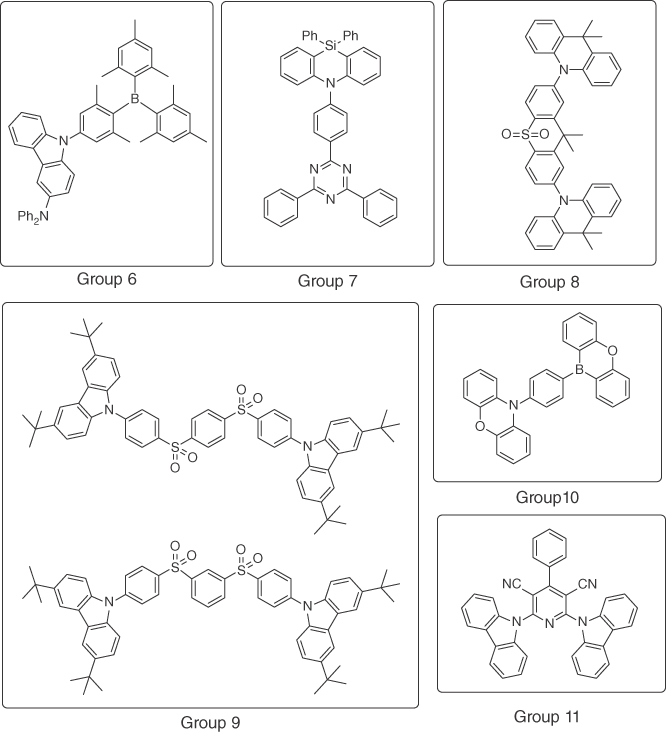
Figure 15.7 Selected structures of published blue TADF emitters (part 2).
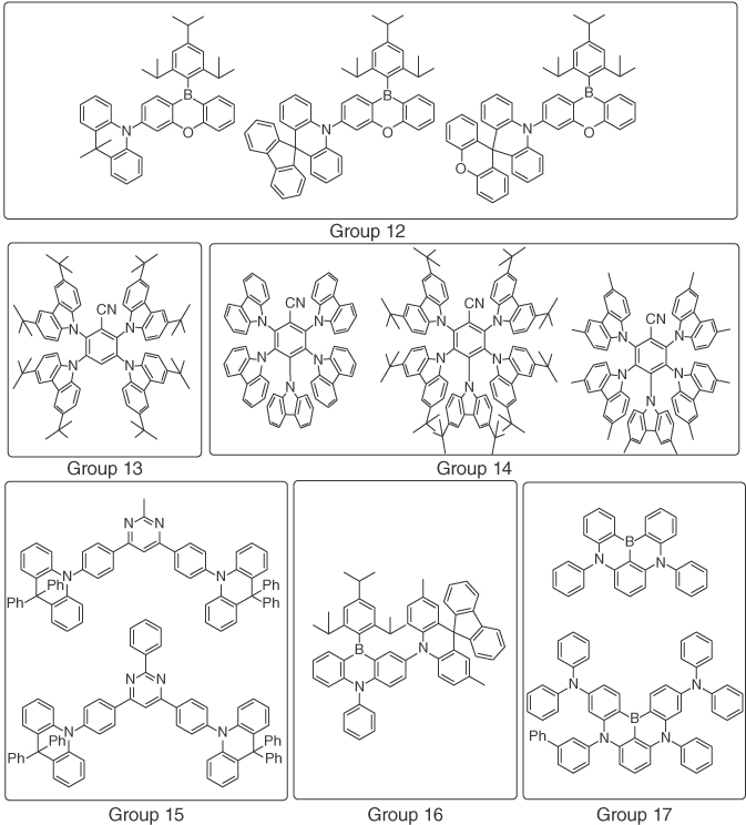
Figure 15.8 Selected structures of published blue TADF emitters (part 3).
Figure 15.9 Selected structures of published blue TADF emitters (part 4).
Figure 15.10 Selected structures of published blue TADF emitters (part 5).
From the collected data, two main conclusions can be derived. First, academic research proves that it should be possible to achieve very high performance with blue TADF technology. Even at very low CIEy coordinates between 0.1 and 0.2, efficiencies in the order of 20% EQE were realized.
Second, there is still a lot of room for improvement. In general, only few academic researchers in the TADF field deal with the degradation, and stability parameters are hardly ever reported. One noteworthy exception is a study by the group of Lian Duan, which reports promising performance values, displayed in Figure 15.11 [77]. These results are in themselves excellent for the device lifetime, compared with what academic researchers published, and among the best in the field looking at color point and efficiency. However, much like most references displayed in Table 15.2, they reveal that the overall stability is still too low for industrial application and that the efficiency roll‐off is strong, reducing the excellent initial efficiency by more than a factor of two at a practical luminance of 500 cd m−2.
Figure 15.11 Performance of 4TCzBN and 5TCzBN. The lifetime was reported at a starting luminance of 500 cd m−2 [77].
Looking at the molecular building blocks, it is apparent that most researchers focus on a narrow set of donor unit that contains triarylamine cores, which are often fused to five‐membered carbazole‐type donors or bridged to six‐membered derivatives. The used bridges range from sp3‐hybridized carbon (→ acridanes) to oxygen and sulfur (→ phenoxazine, phenothiazine) to silicon (→ azasiline). The acceptor units on the other hand cover more chemical space, ranging from aromatic systems substituted with electron‐withdrawing groups to fused nitrogen‐containing heterocycles. Often, other heteroatoms such as sulfur, phosphorous, and boron are found here.
15.2.2 Current Status of Blue TADF Technology: Industry
During the last 2 years, we have witnessed breathtaking improvement of TADF materials, which now can surpass conventional PHOS materials in terms of color point and efficiency, with similar stability. A main driving force behind this progress was the development of suitable screening algorithms for molecular design, which make use of density functional theory (DFT) calculations. These computational tools drastically increased the efficiency of material development by allowing to only synthesize highly efficient TADF materials, thus leading to very short material development cycles with a very steep learning curve per cycle.
Results based on this development approach were recently published by the team at CYNORA [90]. We reported several blue materials, among them a blue emitter reaching 14% EQE at 500 cd m−2 and a lifetime LT80 of 420 h at 500 cd m−2 starting luminance [90]. This material featured an emission maximum below 480 nm.
In here, we briefly discuss the properties of two other recently developed materials, TADF 1 and TADF 2, which are shown in Figures 15.12 and 15.13, as well as Table 15.3.
Figure 15.12 Comparison between photoluminescence (PL) (red curve) of a mid‐blue TADF emitter and its electroluminescence (EL) (blue curve) performance in a bottom‐emitting OLED.
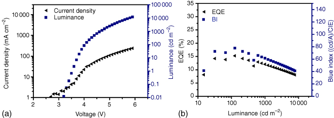
Figure 15.13 Performance of a recent deep‐blue TADF 1 OLED material. (a) Current‐density–voltage characteristics of the device. (b) Dependence of the EQE with luminance. Due to the used host system and stack architecture, a high maximum luminance and low turn‐on voltage are achieved. At a practical luminance of 1000 nits, the EQE is above 12%. However, the device still shows a significant efficiency roll‐off – at 150 nits, a maximum EQE of 15% is reached. This shows that even with the nonoptimized emitter TADF 1, better performance can be expected in an optimized stack architecture.
Table 15.3 Device performance of the CYNORA material (TADF 1) versus Ir(dmp)3, the currently most stable and efficient blue phosphorescent emitter [91], in 13 wt% mCBP (PHOS).
| CIE (1000 nits) | EQE (1000 nits) | Blue indexa * | LT80 (500 nits) | |
| TADF 1 | (0.17, 0.27) | 12% | 78 | 94 |
| PHOS | (0.16, 0.31) | 8% | c. 53 | c. 100 |
aBlue index: calculated by dividing the efficiency in cd A−1 by the CIEy value.
The electrooptic JVL characteristics of this material in a simple device architecture, using the literature‐known host mCBP [92] (short for 4,4′‐bis(3‐methylcarbazol‐9‐yl)‐2,2′‐biphenyl), show a voltage of about 4.2 V at 500 cd m−2. The so‐called blue index, which can be calculated by dividing the current efficiency in cd A−1 and the CIEy color coordinate, approaches 80 at 500 cd m−2 in a bottom‐emitting device.
Ir(dmp)3, short for iridium (III) tris[3‐(2,6‐dimethylphenyl)‐7‐methylimidazo[1,2‐f] phenanthridine], is currently representing one of the most stable blue iridium emitters with a rather blue color point and decent efficiency. In a recent study by Forrest and coworkers [91], the basic performance was reported in the same host used to obtain the data shown in Table 15.3. The LT80 at 500 cd m−2 as well as the blue index of Ir(dmp)3 was estimated from the values given in the publication. Even using a simple, nonoptimized screening architecture and normal R&D‐grade purity, the stability LT80 at this starting luminance is in the order of 100 h, which is in the range of the best phosphorescent materials when also considering the better color and the higher efficiency [91] (Table 15.3). Considering that phosphorescent materials are under investigation since 1997 [6], while TADF has just been studied since 2011 [8], these results demonstrate the breathtaking development curve for TADF.
Moreover, deep‐blue materials with high performance have as well been developed. Emitter TADF 2, for example, displayed performances up to 20% in OLEDs with a CIEy value of 0.17 (Figure 15.14). The efficiency of this emitter reached similarly high performance as the best materials displayed in Table 15.2.

Figure 15.14 The color of OLEDs is measured in the CIE color coordinate system. The blue sector is defined by CIEy values roughly below 0.30 (a). To satisfy the color expectations of the display industry, CIEy values below 0.20, ideally even around CIEy 0.10, will be needed. With current TADF materials, CIEy values in the order of 0.15 can be reached (b). The shown EL spectrum corresponds to CIEy 0.17, which is associated with a peak efficiency of 20% EQE.
15.3 An Alternative Approach: TADF Emitters as (Co) Hosts
15.3.1 General Remarks
Forrest proposed three main approaches to combine both device lifetime and efficiency in blue OLEDs [93]: (i) reducing the excited state lifetime, (ii) reducing the exciton density, and (iii) reducing the effectiveness of bimolecular recombination processes that can promote the excitation to very high energies.
Apart from that, general rules concerning emitter design do apply, too. For example, it is crucial to use robust, stable compounds that are not prone to decomposition or morphological changes such as crystallization, which need to be provided in excellent purity [94].
To understand various aspects of the use of TADF as hosts, it is critical to understand the fundamental differences between Förster‐type and Dexter‐type energy transfer, the two key mechanisms for the energy transfer between two species (Figure 15.15).
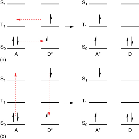
Figure 15.15 Elemental step of the energy transfer according to the mechanisms described by Dexter (a) [95] and Förster (b) [96]. In the Dexter process, electrons are directly exchanged, and the spin of the whole system is conserved, whereas the spin of each species (D and A) is conserved in the Förster process. Because of this, only the Dexter process allows triplet excitons to migrate.
Because of the exchange of electrons during the so‐called Dexter transfer [95], it is mainly important that the distance between two species that are involved in a transfer step is in the order of 0.5–2 nm – for both singlet and triplet excitons. This short‐range transfer is the only way for triplet excitons to migrate. During the transfer, the total spin of the system is conserved. It relies on orbital overlap. The rate for this process can be expressed with
where r is the distance between the species, L the sum of the van der Waals radii of the species, and J the spectral overlap, defined by
The Förster transfer [96] does not rely on a direct exchange of electrons, but on dipole–dipole interaction. The spin of each participating species remains, which allows only singlet excitons to be transferred with this process. The rate for this process can be expressed with
where, in addition to the factors defined above, the radiative decay rate of the donating species, kr, and the photoluminescence quantum yield (PLQY), φ, are of relevance.
The rate is not an exponential function of r, which allows for the Förster process also to occur when r = 20 nm.
15.3.2 First Attempts of Using TADF as Hosts
The fact that energy transfer from TADF molecules to fluorescent emitters is possible was established early: In 2008, Li and coworkers demonstrated that a green‐emitting Cu(I)‐TADF emitter is strongly quenched when introducing a neighboring layer with a low triplet energy. Thus, introducing a DPVBi layer between the TADF‐containing emission layer (EML) and the ETL reduced the efficiency of the device from 16.7 to 5.7 lm W−1 [97]. In 2009, it was shown that the triplet energy of the ETL can affect the efficiency of a TADF OLED due to quenching of TADF triplet excitons by low‐lying triplets of fluorescent molecules [98]. Because of the conceptual analogies between TADF‐type emitters and ambipolar host materials [99–102], it is fair to speculate that the first uses of TADF molecules for host applications were realized unbeknownst to the researchers, which was already discussed elsewhere [10].
Figure 15.16 Materials used in a study by Duan [76]. 4TCzBN was used as the emitter, while 2,6‐2CzBN, 3,5‐2CzBN, 2,4‐2CzBN, and 2,4,6‐3CzBN were evaluated as host materials. All hosts showed a high triplet energy and a good alignment with the HOMO and LUMO energy of 4TCzBN. The best host based on necessary driving voltage was 3,5‐2CzBN, which was attributed to a high PLQY indicated by PL studies, good alignment of frontier orbital energies, and a good ambipolar charge carrier mobility.
15.3.3 Discussion of Various Concepts
Often, the term hyperfluorescence is associated with the use of TADF materials as hosts in OLEDs [65, 103]. This is problematic, since hyperfluorescence was already established several decades ago [104] in medical imaging to describe an increased FLUO during fluorescein angiography, a technique used by ophthalmologists to study the retina.
Also, there are different ways of implementing TADF materials as hosts, which are often described with this term in a confusing manner. Because of this, we will treat the various concepts in separate sections in here.
15.3.3.1 TADF as Host for Other TADF Emitters
Kim and coworkers recently pointed out that the availability of suitable host materials for TADF is somewhat limited, because of the required high triplet energy, in combination with properly adjusted energy levels [105]. Duan and coworkers demonstrated an interesting potential solution to this: By using the same donor and acceptor motifs in emitter and host molecules, devices with high‐efficiency and low driving voltage were realized (Figure 15.16) [76]. It was pointed out that the charge carrier mobility in the EML also needs to be high to bring down the driving voltage.
15.3.3.2 TADF as Host for Fluorescent Materials
Lee and coworkers pointed out a valid issue of this approach: the necessity of a three‐component EML [106]. While the studies discussed in the previous section suggest that it should be possible to technically realize three‐component EMLs where the relative amount of the components differs over three orders of magnitude, transferring them into mass production will be challenging and require optimization of the processing technology. To avoid these costly and elaborate expenses would require two‐component setups of TADF hosts and fluorescent dyes.
In a pioneer work, Duan demonstrated the combination of PIC‐TRZ and DIC‐TRZ, which both emit around 500 nm, with DDAF, an orange‐emitting fluorescent dye that emits at 580 nm (Figure 15.17) [107, 108]. Using Alq3 as a conventional fluorescent host, DDAF gave a peak efficiency in the order of 3% EQE, while the TADF‐type hosts gave a peak efficiency of 11% EQE. In both cases, doping concentrations of 1 wt% were used. In this work, it is proposed to use fluorescent molecules with sterically demanding substituents in future approaches in order to reduce charge trapping on the dopant.

Figure 15.17 Materials used in a study by Duan [107, 108]. PIC‐TRZ and DIC‐TRZ served as TADF‐type host materials, while Alq3 is a fluorescent reference host. The dopant was DDAF, an orange‐emitting fluorescent emitter.
The suitability of TADF materials for host applications seems to be connected to the absence of concentration quenching. While many emitting materials get less efficient at high doping concentrations [109], other materials may actually require high concentrations to emit efficiently (so‐called aggregation‐induced emission (AIE)) [110, 111].
An ideal TADF‐type host material would actually not show any photophysical changes when modifying the concentration. Apart from Cu(I)‐type TADF emitters that are usually devoid of concentration quenching even in neat films or powder [11, 39, 112–114], this issue has been investigated for a great number of metal‐free TADF emitters as well [64, 115, 116].
Interestingly, the presence of DMAC (Figure 15.18) as a donor seems to reduce concentration quenching. While it has been speculated that steric hindrance (resulting in a reduced probability for Dexter transfer processes) could be responsible for this beneficial behavior [117]; this is yet to be investigated systematically.
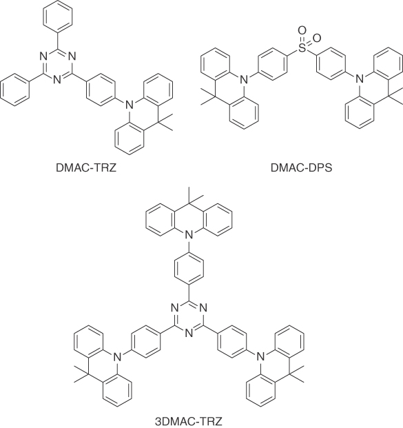
Figure 15.18 Numerous organic TADF emitters have been reported to not show concentration quenching [64, 115, 116]. Often this is connected with the presence of dimethylacridine units as donors.
Just recently, phenoxazine and phenothiazine (Figure 15.19) have been identified as alternatives for DMAC donors, yielding high efficiencies well over 15% EQE and even improved roll‐off behavior in nondoped devices compared with conventional OLEDs with DPEPO as host materals [117].

Figure 15.19 Lee et al. introduced PTSOPT and PTSOPO, two sky blue TADF emitters that were successfully used in efficient, nondoped OLED devices [117].
15.3.3.3 TADF as Host for Phosphorescent Emitters
In addition, TADF‐type hosts were used in combination with phosphorescent emitters [108]. The driving motivation is again the triplet energy: As stated earlier, phosphorescent emitters emit via a transition between the T1 and S0 levels, and, again, the triplet energy of host materials needs to be larger than the triplet energy of the dopant. Especially when moving toward phosphorescent high‐energy emission, TADF emitters are particularly attractive for such applications because of the small singlet–triplet splitting, ΔES1–T1.
A broader review on TADF and ambipolar host materials has been previously published [10]. Some examples are shown in Figure 15.20. D2ACN was published in 2008 in a study describing its use as a host material in red PHOLEDs [118]. After the realization of the beneficial properties of TADF materials as dopants in 2011 [8], the related molecule Spiro‐CN was used in a TADF OLED [119].
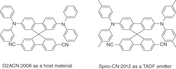
Figure 15.20 D2ACN is a greenish‐yellow TADF‐type host, which was used in combination with a red phosphorescent emitter (10% EQEmax) [118]. Spiro‐CN, a derivative of this molecule, was used as a TADF emitter in combination with a fluorescent host (5% EQEmax) [119].
Figure 15.21 Structures of the phosphorescent emitter PO‐01 and the TADF‐type host BBIC‐TRZ [108].
Combining the orange emitter PO‐01 in 10 wt% concentration with the TADF‐type host BBIC‐TRZ (Figure 15.21) gave excellent performance values with efficiencies in the order of 20% EQE, almost negligible roll‐off up to brightness values of 2000 cd m−2 and a high operational stability of LT50 = 1900 h at 1000 cd m−2 starting luminance under constant current conditions [108]. It is speculated that a potential reason for this surprisingly high stability is the possibility of energy transfer from the host to the dopant via both Förster and Dexter processes. Since TADF hosts are capable of transforming triplet into singlet excitons, a higher ratio of the favorable Förster‐type transfer processes can occur, reducing the triplet exciton density. Interaction between triplet excitons and polarons – so‐called triplet‐polaron quenching (TPQ) – is assumed to be a major degradation pathway in phosphorescent OLEDs [93, 120, 121].
While it seems intriguing to fuse the properties of TADF‐type emitters with the proven performance of phosphorescent materials, there are some drawbacks. For instance, part of the benefits of the metal‐free TADF systems (sustainability, freedom of broad patents, potential cost issues) is lost when combining them with heavy‐metal‐containing systems. Most importantly, since it is not yet proven if the reason for the instability of blue PHOLEDs is tied to the phosphorescent dopant, the hosts, or both, using TADF‐type hosts is no tool to solve any issues based on degradation of the phosphorescent dopants themselves.
15.4 Outlook: What to Expect from TADF Technology in the Future
In 2015, it was already established by CYNORA and others [9] that it is possible to realize a favorable deep‐blue color point with TADF material technology. Recently, great progress toward more stable blue TADF devices was achieved, with emitters featuring emission below 480 nm, 14% external quantum efficiency, and lifetime values LT80 of 420 h (measured at 500 cd m−2 brightness) [90]. Within a relatively short period of R&D, TADF emitters have now reached a similar performance to PHOS emitters with a blue color point. The cornerstone of these successes was a fast translation of quantum chemical predictions from DFT calculations into material design and a continuous improvement of the underlying theory, which leads to improved materials in each learning cycle. Following this trend, blue TADF technology can reach market readiness in the very near future.
Further improvement can be expected through the realization of more sophisticated stack architectures: It is known that mCBP, a component used in the aforementioned early‐stage devices, features several stability issues, potentially limiting the stability of these OLEDs [122]. Thus, the use of alternative, more stable hosts will lead to even longer lifetimes.
Nevertheless, it is also clear that the basic stability of both the materials and the stack architectures still needs to be improved fundamentally. Looking back at a very steep learning curve displayed by research‐driven companies such as CYNORA, as well as the great academic progress [77, 105, 123], this necessary advancement seems achievable in a short amount of time. TADF will contribute to the next material‐driven advancement of the OLED industry, making OLEDs ready for even more applications soon.
References
- 1 Tang, C.W. and VanSlyke, S.A. (1987). Appl. Phys. Lett. 51: 913.
- 2 Volz, D., Wallesch, M., Fléchon, C., Danz, M., Verma, A., Navarro, J.M., Zink, D.M., Bräse, S., and Baumann, T. (2015). Green Chem. 17: 1988–2011.
- 3 Shinar, J. (2003). Organic Light‐Emitting Devices: A Survey. Springer‐Verlag.
- 4 Yersin, H., Finkenzeller, W.J., Walter, M.J., Djurovich, P.I., Thompson, M.E., Tsuboyama, T., Akira, S.O., Ueno, K., Chi, Y., Chou, P.‐T., Yang, X.‐H., Jaiser, F., Neher, D., Xiang, H.‐F., LAi, S.‐W., Lai, P.T., Che, C.‐M., Tanaka, I., Tokito, S., Van Dijken, A., Brunner, K., Börner, H., Langeveld, B.M.W., Mak, C.S.K., Nazeeruddin, M.K., Klein, C., Grätzel, M., Zuppiroli, L., Berner, D., Bian, Z.‐Q., and Huang, C.‐H. (2008). Highly Efficient OLEDs with Phosphorescent Materials, 1e. Wiley‐VCH.
- 5 Van Slyke, S.A., Chen, C.H., and Tang, C.W. (1996). Appl. Phys. Lett. 69: 2160.
- 6 Baldo, M.A., O'Brian, Y., You, A., Shoustikov, A., Sibley, S., Thompson, M.E., and Forrest, S.R. (1998). Nature 395: 151–154.
- 7 Baldo, M.A., Lamansky, S., Burrows, P.E., Thompson, M.E., and Forrest, S.R. (1999). Appl. Phys. Lett. 75: 4.
- 8 Endo, A., Sato, K., Yoshimura, K., Kai, T., Kawada, A., Miyazaki, H., and Adachi, C. (2011). Appl. Phys. Lett. 98: 083302.
- 9 Bergmann, L., Zink, D.M., Bräse, S., Baumann, T., and Volz, D. (2016). Top. Curr. Chem. 374: 22.
- 10 Volz, D. (2016). J. Photonics Energy 6: 020901.
- 11 Yersin, H., Rausch, A.F., Czerwieniec, R., Hofbeck, T., and Fischer, T. (2011). Coord. Chem. Rev. 255: 2622–2652.
- 12 Yersin, H. and Monkiwius, U. (2008). DE 102008033563 A1.
- 13 McCarthy, J.T. (1995). McCarthy's Desk Encyclopedia of Intellectual Property, Bureau of National Affars, 3e.
- 14 Krebs, F.C. (2009). Sol. Energy Mater. Sol. Cells 93: 394–412.
- 15 Smith, A.R.G., Lee, K.H., Nelson, A., James, M., Burn, P.L., and Gentle, I.R. (2012). Adv. Mater. 24: 822–826.
- 16 Zuniga, C.A., Barlow, S., and Marder, S.R. (2011). Chem. Mater. 23: 658–681.
- 17 Yoon, Y., Lee, H., Kim, T., Kim, K., Choi, S., Yoo, H.K., Friedman, B., and Lee, K. (2013). Solid State Electron. 79: 45–49.
- 18 Höfle, S., Pfaff, M., Do, H., Bernhard, C., Gerthsen, D., Lemmer, U., and Colsmann, A. (2014). Org. Electron. 15: 337–341.
- 19 Kaake, L.G., Barbara, P.F., and Zhu, X.‐Y. (2010). J. Phys. Chem. Lett. 1: 628–635.
- 20 Meyers, A. and Weck, M. (2004). Chem. Mater. 16: 1183–1188.
- 21 Volz, D., Baumann, T., Flügge, H., Mydlak, M., Grab, T., Bächle, M., Barner‐Kowollik, C., and Bräse, S. (2012). J. Mater. Chem. 22: 20786.
- 22 Moad, G., Chen, M., Häussler, M., Postma, A., Rizzardo, E., and Thang, S.H. (2011). Polym. Chem. 2: 492.
- 23 Furuta, P.T., Deng, L., Garon, S., Thompson, M.E., and Fréchet, J.M.J. (2004). J. Am. Chem. Soc. 126: 15388–15389.
- 24 Gao, H., Poulsen, D.A., Ma, B., Unruh, D.A., Zhao, X., Millstone, J.E., and Fréchet, J.M.J. (2010). Nano Lett. 10: 1440–1444.
- 25 Ma, B., Lauterwasser, F., Deng, L., Zonte, C.S., Kim, B.J., Fréchet, J.M.J., Borek, C., and Thompson, M.E. (2007). Chem. Mater. 19: 4827–4832.
- 26 Wang, X.‐Y., Kimyonok, A., and Weck, M. (2006). Chem. Commun. (Camb.) 3933–3935.
- 27 Volz, D., Hirschbiel, A.F., Zink, D.M., Friedrichs, J., Nieger, M., Baumann, T., Bräse, S., and Barner‐Kowollik, C. (2014). J. Mater. Chem. C 2: 1457.
- 28 Nuyken, O., Jungermann, S., Wiederhirn, V., Bacher, E., and Meerholz, K. (2006). Monatsh. Chem. Chem. Mon. 137: 811–824.
- 29 Nuyken, O., Bacher, E., Braig, T., Fáber, R., Mielke, F., Rojahn, M., Wiederhirn, V., Meerholz, K., and Müller, D. (2002). Des. Monomers Polym. 5: 195–210.
- 30 Gather, M.C., Köhnen, A., Falcou, A., Becker, H., and Meerholz, K. (2007). Adv. Funct. Mater. 17: 191–200.
- 31 Köhnen, A., Riegel, N., Kremer, J.H.‐W.W.M., Lademann, H., Müller, D.C., and Meerholz, K. (2009). Adv. Mater. 21: 879–884.
- 32 Zhong, C., Liu, S., Huang, F., Wu, H., and Cao, Y. (2011). Chem. Mater. 23: 4870–4876.
- 33 Gu, C., Fei, T., Yao, L., Lv, Y., Lu, D., and Ma, Y. (2011). Adv. Mater. 23: 527–530.
- 34 Baba, A., Onishi, K., Knoll, W., and Advincula, R.C. (2004). J. Phys. Chem. B 108: 18949–18955.
- 35 Huyal, I.O., Koldemir, U., Ozel, T., Demir, H.V., and Tuncel, D. (2008). J. Mater. Chem. 18: 3568.
- 36 Liaptsis, G. and Meerholz, K. (2013). Adv. Funct. Mater. 23: 359–365.
- 37 Liaptsis, G., Hertel, D., and Meerholz, K. (2013). Angew. Chem. 52: 9563–9567.
- 38 Zink, D.M., Baumann, T., Nieger, M., and Bräse, S. (2011). Eur. J. Org. Chem. 2011: 1432–1437.
- 39 Czerwieniec, R., Yu, J., and Yersin, H. (2011). Inorg. Chem. 50: 8293–8301.
- 40 Zink, D.M., Grab, T., Baumann, T., Nieger, M., Barnes, E.C., Klopper, W., and Bräse, S. (2011). Organometallics 30: 3275–3283.
- 41 Anastas, P.T. and Warner, J.C. (1998). Green Chemistry: Theory and Practice. New York: Oxford University Press.
- 42 U. S. Environmental Protection Agency and U. S. Office of Resource Conservation and Recovery (2011). Electronics Waste Management in the United States Through 2009.
- 43 Peiró, L.T., Méndez, G.V., and Ayres, R.U. (2013). Environ. Sci. Technol. 47: 2939–2947.
- 44 Jackson, B. and Mikolajczak, C. (2011). Availability of Indium and Gallium. Indium Corporation.
- 45 Mudd, G.M. (2012). Ore Geol. Rev. 46: 106–117.
- 46 Henderson, P. and Henderson, G.M. (2009). The Cambridge Handbook of Earth Science Data. Cambridge University Press.
- 47 Libourel, G. and Corrigan, C.M. (2014). Elements 10: 11–17.
- 48 U.S. Geological Survey (2007). Mineral Commodity Summaries. U.S. Geological Survey.
- 49 Brenan, J.M. (2008). Elements 4: 227–232.
- 50 Angerer, G., Marscheider‐Weidemann, F., Lüllmann, A., Erdmann, L., Scharp, M., Handke, V., and Marwede, M. (2009). Rohstoffe für Zukunftstechnologien: Einfluss des branchenspezif ischen Rohstoffbedarfs in rohstoffintensiven Zukunftstechnologien auf die zukünftige Rohstoffnachfrage. Institut für Zukunftsstudien und Technologiebewertung IZT gGmbH.
- 51 Chancerel, P., Rotter, V.S., Ueberschaar, M., Marwede, M., Nissen, N.F., and Lang, K.‐D. (2013). Waste Manage. Res. 31: 3–16.
- 52 Binnemans, K., Jones, P.T., Blanpain, B., Van Gerven, T., Yang, Y., Walton, A., and Buchert, M. (2013). J. Cleaner Prod. 51: 1–22.
- 53 Manhart, A., Buchert, M., Bleher, D., and Pingel, D. (2012). Electronics Goes Green 2012+ (EGG), pp. 1–5.
- 54 Trezona, P.W. (2001). Color Res. Appl. 26: 67–75.
- 55 dos Santos, P.L., Ward, J.S., Bryce, M.R., and Monkman, A.P. (2016). J. Phys. Chem. Lett. 7: 3341–3346.
- 56 Bocksrocker, T., Eschenbaum, C., Preinfalk, J.B., Hoffmann, J., Asche‐Tauscher, J., Maier‐Flaig, F., and Lemmer, U. (2012). Renewable Energy and the Environment Optics and Photonics Congress, LM3A.4. Washington, DC: Optical Society of America.
- 57 Zhang, X.‐W., Liu, L.‐M., Li, J., Zhang, L., Jiang, X.‐Y., Zhang, Z.‐L., Wang, H., and Liu, X.‐Y. (2011). J. Disp. Technol. 7: 515–519.
- 58 Komino, T., Tanaka, H., and Adachi, C. (2014). Chem. Mater. 26: 3665–3671.
- 59 Kuma, H. and Hosokawa, C. (2014). Sci. Technol. Adv. Mater. 15: 034201.
- 60 Zhu, M. and Yang, C. (2013). Chem. Soc. Rev. 42: 4963–4976.
- 61 Li, K., Liu, M., Yang, S., Chen, Y., He, Y., Murtaza, I., Goto, O., Shen, C., Meng, H., and He, G. (2017). Dyes Pigm. 139: 747–755.
- 62 Li, Y., Liu, J.‐Y., Zhao, Y.‐D., and Cao, Y.‐C. (2017). Mater. Today 20 (5): 258–266.
- 63 Murawski, C., Leo, K., and Gather, M.C. (2013). Adv. Mater. 25: 6801–6827.
- 64 Zhang, Q., Li, J., Shizu, K., Huang, S., Hirata, S., Miyazaki, H., and Adachi, C. (2012). J. Am. Chem. Soc. 134: 14706–14709.
- 65 Lee, S.Y., Yasuda, T., Yang, Y.S., Zhang, Q., and Adachi, C. (2014). Angew. Chem. Int. Ed. 53: 6402–6406.
- 66 Reineke, S. (2014). Nat. Photonics 8: 269–270.
- 67 Hirata, S., Sakai, Y., Masui, K., Tanaka, H., Lee, S.Y., Nomura, H., Nakamura, N., Yasumatsu, M., Nakanotani, H., Zhang, Q., Shizu, K., Miyazaki, H., and Adachi, C. (2014). Nat. Mater. 14: 1–37.
- 68 Kim, M., Jeon, S.K., Hwang, S., and Lee, J.Y. (2015). Adv. Mater. 27: 1–6.
- 69 Suzuki, K., Kubo, S., Shizu, K., Fukushima, T., Wakamiya, A., Murata, Y., Adachi, C., and Kaji, H. (2015). Angew. Chem. Int. Ed. 54: 15231–15235.
- 70 Sun, J.W., Baek, J.Y., Kim, K.‐H., Moon, C.‐K., Lee, J.‐H., Kwon, S.‐K., Kim, Y.‐H., and Kim, J.‐J. (2015). Chem. Mater. 27: 6675–6681.
- 71 Lee, I. and Lee, J.Y. (2016). Org. Electron. 29: 160–164.
- 72 Liu, M., Seino, Y., Chen, D., Inomata, S., Su, S., Sasabe, H., and Kido, J. (2015). Chem. Commun. 51: 16353–16356.
- 73 Kitamoto, Y., Namikawa, T., Ikemizu, D., Miyata, Y., Suzuki, T., Kita, H., Sato, T., and Oi, S. (2015). J. Mater. Chem. C 3: 9122–9130.
- 74 Liu, W., Zheng, C.‐J., Wang, K., Chen, Z., Chen, D.‐Y., Li, F., Ou, X.‐M., Dong, Y.‐P., and Zhang, X.‐H. (2015). ACS Appl. Mater. Interfaces 7: 18930–18936.
- 75 Numata, M., Yasuda, T., and Adachi, C. (2015). Chem. Commun. 51: 9443–9446.
- 76 Zhang, D., Cai, M., Bin, Z., Zhang, Y., Zhang, D., and Duan, L. (2016). Chem. Sci. 7: 3355–3363.
- 77 Zhang, D.D., Cai, M., Zhang, Y., Zhang, D.D., and Duan, L. (2016). Mater. Horiz. 3: 145–151.
- 78 Park, I.S., Lee, J., and Yasuda, T. (2016). J. Mater. Chem. C 4: 7911–7916.
- 79 Park, I.S., Numata, M., Adachi, C., and Yasuda, T. (2016). Bull. Chem. Soc. Jpn. 89: 375–377.
- 80 Hatakeyama, T., Shiren, K., Nakajima, K., Nomura, S., Nakatsuka, S., Kinoshita, K., Ni, J., Ono, Y., and Ikuta, T. (2016). Adv. Mater. 28: 2777–2781.
- 81 Noda, H., Kabe, R., and Adachi, C. (2016). Chem. Lett. 45: 1463–1466. doi: 10.1246/cl.160814.
- 82 Kim, M., Choi, J.M., and Lee, J.Y. (2016). Chem. Commun. 52: 10032–10035.
- 83 Park, I.S., Komiyama, H., and Yasuda, T. (2017). Chem. Sci. 8: 953–960.
- 84 Cui, L.‐S., Nomura, H., Geng, Y., Kim, J.U., Nakanotani, H., and Adachi, C. (2017). Angew. Chem. Int. Ed. 56: 1571–1575.
- 85 Cho, Y.J., Jeon, S.K., Lee, S.S., Yu, E., and Lee, J.Y. (2016). Chem. Mater. 28: 5400–5405.
- 86 Duan, C., Li, J., Han, C., Ding, D., Yang, H., Wei, Y., and Xu, H. (2016). Chem. Mater. 28: 5667–5679.
- 87 Sun, J.W., Baek, J.Y., Kim, K.‐H., Huh, J.‐S., Kwon, S.‐K., Kim, Y.‐H., and Kim, J.‐J. (2017). J. Mater. Chem. C 5: 1027–1032.
- 88 Komatsu, R., Ohsawa, T., Sasabe, H., Nakao, K., Hayasaka, Y., and Kido, J. (2017). ACS Appl. Mater. Interfaces 9: 4742–4749. doi: 10.1021/acsami.6b13482.
- 89 Cha, J.‐R., Lee, C.W., and Gong, M.‐S. (2017). Dyes Pigm. 140: 399–406.
- 90 Press release (October 2016). www.cynora.com.
- 91 Zhang, Y., Lee, J., and Forrest, S.R. (2014). Nat. Commun. 5: 1–7.
- 92 Li, G., Fleetham, T., Turner, E., Hang, X.C., and Li, J. (2015). Adv. Opt. Mater. 3: 390–397.
- 93 Forrest, S.R. (2015). Philos. Trans. R. Soc. A: Math. Phys. Eng. Sci. 373: 20140320.
- 94 Fujimoto, H., Suekane, T., Imanishi, K., Yukiwaki, S., Wei, H., Nagayoshi, K., Yahiro, M., and Adachi, C. (2016). Sci. Rep. 6: 38482.
- 95 Dexter, D.L. (1953). J. Chem. Phys. 21: 836.
- 96 Förster, T. (1948). Ann. Phys. 437: 55–75.
- 97 Su, Z., Li, W., Chu, B., Xu, M., Che, G., Wang, D., Han, L., Li, X., Zhang, D., Bi, D., and Chen, Y. (2008). J. Phys. D: Appl. Phys. 41: 085103.
- 98 Zhang, Q., Komino, T., Huang, S., Matsunami, S., Goushi, K., and Adachi, C. (2012). Adv. Funct. Mater. 22: 2327–2336.
- 99 Leung, M., Hsieh, Y.‐H., Kuo, T., Chou, P.‐T., Lee, J.‐H., Chiu, T.‐L., and Chen, H.‐J. (2013). Org. Lett. 15: 4694–4697.
- 100 Kim, D., Zhu, L., and Brédas, J.‐L. (2012). Chem. Mater. 24: 2604–2610.
- 101 Wagner, D., Hoffmann, S.T., Heinemeyer, U., Münster, I., Köhler, A., Strohriegl, P., Ho, S.T., Mu, I., and Ko, A. (2013). Chem. Mater. 25: 3758–3765.
- 102 Takizawa, S., Montes, V.A., and Anzenbacher, P. (2009). Synthesis (Stuttg) 2452–2458.
- 103 Adachi, C. (2013). SID Symp. Dig. Tech. Pap. 44: 513–514.
- 104 Turner, R.G., James, D.G., Friedmann, A.I., Vijendram, M., and Davies, J.P. (1975). Br. J. Ophthalmol. 59: 657–663.
- 105 Sun, J.W., Kim, K.‐H., Moon, C.‐K., Lee, J.‐H., and Kim, J.‐J. (2016). ACS Appl. Mater. Interfaces 8: 9806–9810.
- 106 Song, W., Lee, I., and Lee, J.Y. (2015). Adv. Mater. 27: 4358–4363.
- 107 Zhang, D., Duan, L., Li, C., Li, Y., Li, H., Zhang, D., and Qiu, Y. (2014). Adv. Mater. 26: 5050–5055.
- 108 Duan, L. (2015). SID Symp. Dig. Tech. Pap. 2: 498–501.
- 109 Zhang, Y.Q., Zhong, G.Y., and Cao, X.A. (2010). J. Appl. Phys. 108: 083107.
- 110 Li, J., Jiang, Y., Cheng, J., Zhang, Y., Su, H., Lam, J.W.Y., Sung, H.H.Y., Wong, K.S., Kwok, H.S., and Tang, B.Z. (2014). Phys. Chem. Chem. Phys. 17: 1134–1141.
- 111 Hong, Y., Lam, J.W.Y., and Tang, B.Z. (2011). Chem. Soc. Rev. 40: 5361–5388.
- 112 Flügge, H., Rohr, A., Döring, S., Fléchon, C., Wallesch, M., Zink, D., Seeser, J., Leganés, J., Sauer, T., Rabe, T., Kowalsky, W., Baumann, T., and Volz, D. (2015). Reduced concentration quenching in a TADF‐type copper(I)‐emitter. Proc. SPIE 9566, Organic Light Emitting Materials and Devices XIX, 95661P (22 September 2015). doi: 10.1117/12.2185935.
- 113 Wallesch, M., Volz, D., Zink, D.M., Schepers, U., Nieger, M., Baumann, T., and Bräse, S. (2014). Chem. Eur. J. 20: 6578–6590.
- 114 Volz, D., Zink, D.M., Bocksrocker, T., Friedrichs, J., Nieger, M., Baumann, T., Lemmer, U., and Bräse, S. (2013). Chem. Mater. 25: 3414–3426.
- 115 Wada, Y., Shizu, K., Kubo, S., Fukushima, T., Miwa, T., Tanaka, H., Adachi, C., and Kaji, H. (2016). Appl. Phys. Express 9: 032102.
- 116 Zhang, Q., Tsang, D., Kuwabara, H., Hatae, Y., Li, B., Takahashi, T., Lee, S.Y., Yasuda, T., and Adachi, C. (2015). Adv. Mater. 27: 2096–2100.
- 117 Lee, I.H., Song, W., and Lee, J.Y. (2016). Org. Electron. 29: 22–26.
- 118 Hung, W.‐Y., Tsai, T.‐C., Ku, S.‐Y., Chi, L.‐C., and Wong, K.‐T. (2008). Phys. Chem. Chem. Phys. 10: 5822.
- 119 Nakagawa, T., Ku, S.‐Y., Wong, K.‐T., and Adachi, C. (2012). Chem. Commun. 48: 9580.
- 120 van Eersel, H., Bobbert, P.A., Janssen, R.A.J., and Coehoorn, R. (2014). Appl. Phys. Lett. 105: 143303.
- 121 Coehoorn, R., Van Eersel, H., Bobbert, P.A., and Janssen, R.A.J. (2015). Adv. Funct. Mater. 25: 2024–2037.
- 122 Klubek, K.P., Tang, C.W., and Rothberg, L.J. (2014). Org. Electron. 15: 1312–1316.
- 123 Nakanotani, H., Masui, K., Nishide, J., Shibata, T., and Adachi, C. (2013). Sci. Rep. 3: 2127.