
14
Solution‐Processed TADF Materials and Devices Based on Organic Emitters
Nidhi Sharma1,2, Michael Yin Wong1, Ifor D.W. Samuel2, and Eli Zysman‐Colman1
1University of St Andrews, Organic Semiconductor Centre, EaStCHEM School of Chemistry, St Andrews, KY16 9ST, Fife, UK
2University of St Andrews, Organic Semiconductor Centre, SUPA School of Physics and Astronomy, St Andrews, KY16 9SS, Fife, UK
14.1 Introduction
Since the seminal discovery of electroluminescence (EL) in a bilayer organic light‐emitting diode (OLED) by Tang and VanSlyke [1], OLEDs have blossomed over the last three decades due to their enormous potential in flat‐panel display and solid‐state lighting (SSL) applications. Compared with existing liquid crystal displays (LCDs), OLED displays give high contrast and viewing angle, together with high brightness and vivid colors. In addition, OLED displays provide low power usage, the capacity to display true black, a more robust, and environmentally friendly design than LCD screens. An extensive worldwide research and development effort has brought OLED technology to global adoption for displays, and the first commercial lighting devices are available.
OLEDs produce light when a voltage is applied to them, leading to the injection of charges. The injected electrons and holes can combine to form an exciton (bound electron‐hole pair). The spin of the two charges can be combined in four ways, leading to 25% of the excitons formed under electrical excitation being in the singlet spin state and 75% triplets [2]. In fluorescent materials, electrically generated triplet excitons dissipate their energy in the form of heat resulting in a theoretical limit of 25% internal quantum efficiency (IQE). Taking into account a light‐outcoupling efficiency of ca. 20% in a typical OLED, this results in a maximum external quantum efficiency (EQE) of 5% for the device. Even though a higher proportion of singlets has been suggested in conjugated polymers [3], triplet formation is nevertheless a major loss mechanism that needs to be overcome for highly efficient devices.
To increase the IQE limit of the OLED, phosphorescent materials were developed to harvest the nonemissive triplet excitons [4]. Phosphorescence is achieved through the use of organometallic complexes that incorporate a heavy metal. Its presence facilitates a rapid intersystem crossing (ISC) as a result of the large spin–orbit coupling (SOC) constant associated with the metal. Likewise, SOC induced by the heavy metal enhances radiative decay from the excited triplet state to the singlet ground state. Using this approach, both singlet and triplet excitons are harvested, which in turn leads to 100% IQE. Indeed, OLEDs employing phosphorescent metal complex emitters have been shown to exhibit EQEs of over 30% [5]. The majority of these highly efficient phosphorescent materials are based on scarce and expensive iridium(III) and platinum(II) complexes. In order to achieve a truly inexpensive OLED technology, a paradigm shift in materials development is required. Innovative design strategies relying on triplet–triplet annihilation (TTA) [6] or thermally activated delayed fluorescence (TADF) [7] have emerged in recent years. The maximum IQE for TTA is 62.5%, whereas for TADF it is a tantalizing 100%. TADF‐based materials development has progressed rapidly since the first report of a TADF material used in an OLED in 2009 [8]. Recruitment of triplet excitons in TADF materials occurs through their conversion to singlet excitons through a rapid reverse intersystem crossing (rISC) made possible by a vanishingly small singlet–triplet excited‐state energy difference (ΔEST). Small ΔEST values (usually defined as <200 meV) are achieved when the HOMO–LUMO exchange integral is small, which occurs when the HOMO and LUMO are spatially separated. Examples of OLEDs using noble metal‐free TADF emitters have already achieved EQEs of over 30% in the blue [5b] and green [5a] and close to 19% in red [9] devices, demonstrating their great potential as replacements for high‐efficiency phosphorescent OLEDs [10].
Generally, the fabrication of OLEDs has been categorized into one of two approaches: Thermal evaporation under vacuum is predominantly used for small molecule‐based OLEDs [11]; for polymeric [12] and dendrimeric materials [13], solution processing techniques such as spin‐coating and inkjet printing are employed [14]. Most OLEDs based on TADF emitters possess a vacuum‐evaporated multilayer architecture. Careful choice of these layers permits optimal charge injection and transport and exciton recombination kinetics leading to high‐efficiency devices. However, the complexity, inefficiency of materials use, and cost of vacuum deposition limit the mass production of cost‐effective OLEDs, which is particularly germane for SSL applications [15]. Solution‐processed OLEDs on the other hand hold great promise for reducing in dramatic fashion the fabrication cost of the device, particularly when it comes to pixel patterning and large area OLEDs [16]. Inkjet and roll‐to‐roll printing can effectively be used to fabricate large area high‐resolution full‐color flat‐panel displays; these fabricated onto a wide range of substrates including flexible plastic and metal foil [17].
In general, for a solution‐processed OLED material, it is necessary to have a uniform, amorphous film. Light‐emitting polymers have been the most intensively studied on this platform [14a, 18], though the performance metrics of OLEDs employing polymers are typically lower than those using thermally deposited small molecules. Over the past few years, the device efficiency and lifetime of polymer‐based devices has improved to the point of being attractive candidates for commercial OLED devices [14a]. There remain still some intrinsic challenges when using polymeric materials such as batch‐to‐batch variation and purification of the polymers. Light‐emitting dendrimers were developed as an alternative class of solution‐processed material, although macromolecular are also monodisperse. In this approach the core of the dendrimer defines the key electronic properties (e.g. color of light emission), while conjugated dendrons keep the cores apart and surface groups confer solubility [19]. In this way a very wide range of chromophores can be made solution processable, and their aggregation controlled [20]. Solution‐processed small molecules are also attractive because they too have well‐defined molecular structures, reproducibility of their synthesis, and facile purification. Thus, it is a good strategy to develop OLEDs based on solution‐processable small molecules. Unfortunately, the majority of the small molecule emitters designed for vacuum deposition are not suitable for the solution processing due to their poor film morphology and easy crystallization upon spin casting. Device performance of such small molecule solution‐processed OLEDs remains inferior to that of vacuum‐deposited OLEDs [16].
The evolution of the development of solution‐processed OLEDs mirrors that of vacuum‐deposited OLEDs and started with polymers [12] and dendrimers [13, 19a], and then systems based on fluorescent [1] small molecules [21] were developed. Phosphorescent materials replaced fluorescent analogues in vacuum‐deposited devices in order to achieve higher device efficiencies [4]. In the phosphorescent‐based solution‐processed OLEDs, device performance was enhanced by using dendrimers to confer solubility and control aggregation, leading to an EQE of 16% and green emission for the device. Soluble hosts and phosphorescent light‐emitting materials [15a, 20, 22] have also achieved highly efficient solution‐processed devices – a small molecule host and dopant materials for vacuum‐deposited phosphorescent OLEDs were modified or used without modifications. Using this approach, EQEs close to 20% were reported for red [15a, 22a, 23], green [22b, 24], and blue [22c, d, 25, phosphorescent OLEDs, which were comparable with their vacuum‐deposited counterparts.
Although most of the studies for achieving highly efficient devices have been focused on the development of solution‐processable phosphorescent materials, recent progress in TADF materials has opened up the possibility for the development of high‐efficiency solution‐processed OLEDs using this class of materials. Figure 14.1 shows the comparison of the maximum EQEs achieved for green‐emitting TADF OLEDs fabricated by vacuum deposition and solution processing over the past 5 years, the data of which were obtained at their turn‐on voltages (∼1–5 cd m−2 brightness). Although it is well established in OLED development to quote the efficiencies at display brightnesses (e.g. 100 cd m−2), surprisingly in the field of TADF materials, many papers do not do this. Since the first report of a solution‐processed TADF emitter in late 2014 [26], the field has progressed rapidly, and already EQEs comparable to those of highly efficient vacuum‐deposited TADF emitters have been achieved.

Figure 14.1 Chronological comparison of maximum EQEs achieved in OLEDs using green TADF emitters.
In this review, we discuss the development of purely organic (i.e. metal‐free) small molecule organic solution‐processed TADF materials and their use in OLED devices and compare their performance with the state‐of‐the‐art vacuum‐deposited TADF materials and devices. Solution‐processed TADF polymers and dendrimers are also discussed, and their device performance is contrasted with small molecule solution‐processed TADF OLEDs.
14.1.1 Solution‐Processed Blue TADF Materials and Devices
The color of an OLED is defined by its Commission Internationale de l'Éclairage (CIE) coordinates. For a pure blue emitter, standard CIE coordinates defined by the National Television System Committee (NTSC) are (0.14, 0.08), whereas Phase Alternating Line (PAL) systems define pure blue color by CIE coordinates of (0.15, 0.06). Not all reports in the literature document CIE coordinates, and so in this chapter we have taken a simplified definition of blue emitters to be those materials with EL maxima (λEL) shorter than 490 nm. The photophysical properties of blue emitters 1–8 and EL characteristics of the corresponding OLEDs are summarized in Tables 14.1 and 14.2, respectively. The first report of a solution‐processed blue TADF emitter was published by Mei et al. in 2015 [27]. They employed an inductively electron‐withdrawing trifluoromethyl (‐CF3) group as the acceptor with weakly donating carbazole donors in compounds 1 (4CzCF3Ph) and 2 (5CzCF3Ph). Compound 1 exhibited blue emission with emission maxima, λPL, at 442 nm in toluene and 445 nm in a thin film consisting of 10 wt% 1 doped in mCP. With an additional carbazole donor, 2 displayed a redshifted emission with λPL at 475 nm in toluene and 495 nm in a thin film consisting of 10 wt% 2 doped in mCP. Both the compounds exhibited microsecond delayed emission decays, τd, of 9.31 μs for 1 and 15.33 μs for 2 in degassed toluene solution, indicating the emission was delayed fluorescence. The photoluminescence quantum yields, ΦPL, for 1 and 2 in toluene are 13% and 24%, respectively, under ambient conditions, which increased to 24% and 43%, respectively, under oxygen‐free conditions. The ΔEST, determined from the energy difference of the highest energy vibronic subbands of the 77 K fluorescence and phosphorescence spectra, was found to be 0.24 eV for 1 and 0.02 eV for 2, suggesting more efficient rISC in 2 than in 1. Solution‐processed devices were fabricated using the device stack: indium tin oxide (ITO)/poly(3,4‐ethylenedioxythiophene)polystyrene sulfonate (PEDOT:PSS) (40 nm)/mCP:10 wt% 1 or 2 (40 nm)/TmPyPB (60 nm)/LiF (0.8 nm)/Al (100 nm). Compounds 1 and 2 exhibited λEL of 464 and 484 nm with CIE coordinates of (0.17, 0.18) and (0.21, 0.33), respectively. Devices based on 2 showed a maximum EQE of 5.2% with luminance and current efficiency of 2436 cd m−2 and 11.6 cd A−1, respectively, whereas for 1 these values decreased to 1032 cd m−2 and 1.03 cd A−1 with an EQE of 0.67%. The significantly higher device efficiency for 2 was attributed to its significantly smaller ΔEST (Figure 14.2).
One of the key factors in achieving highly efficient solution‐processed TADF OLEDs is to improve the solubility of the emitters in organic solvents. To address this issue, Lee and coworkers [28] reported fluorine‐substituted benzonitrile acceptor‐based TADF emitters 3 (3CzFCN) and 4 (4CzFCN) with improved solubility and blue emission color. The design principles for 3 and 4 were almost identical to those of 1 and 2. Here, the authors replaced the trifluoromethylbenzene acceptor with difluorobenzonitrile/fluorobenzonitrile acceptors. Improvement in the solubility of 3 and 4 in dichloromethane and blue emission was attributed to the hydrophobic and weak electron‐withdrawing nature of the F atom, respectively. Both 3 and 4 show a remarkably small ΔEST of 0.06 eV. Compound 3 emits at 443 nm with a ΦPL of 76% in 10 wt% CzSi thin film, while the λPL for 4 is 453 nm but with remarkable 100% ΦPL under oxygen‐free conditions. Their solution‐processed devices were fabricated using the following device structure: ITO/PEDOT:PSS (60 nm)/PVK (15 nm)/CzSi:10 wt% 3 or 15 wt% 4 (25 nm)/TSPO1 (5 nm)/TPBi (30 nm)/LiF (1 nm)/Al (100 nm). OLED devices showed blue emission with λEL of 463 and 471 nm and CIE coordinates of (0.16, 0.19) and (0.16, 0.25) for 3 and 4, respectively. At the same time, vacuum‐deposited devices for 3 and 4 were also fabricated for comparison with device structures of ITO/NPB(35 nm)/CzSi:10 wt% 3 or 4 15 wt% (20 nm)/TSPO1 (5 nm)/TPBi (30 nm)/LiF(1 nm)/Al (100 nm). The solution‐processed devices were highly efficient with excellent maximum EQEs of 17.8% (8% at 100 cd m−2) for 3 and 20% (16.3% at 100 cd m−2) for 4, which were higher than their vacuum‐deposited counterparts (maximum EQE of 12.9% (10.9% at 100 cd m−2) for 3, EQE of 17.3% (12.3% at 100 cd m−2) for 4). These examples represent the highest reported EQE values for solution‐processed blue TADF devices to date (Figure 14.3).

Figure 14.2 Chemical structures of emitters 1 and 2.
Table 14.1 Photophysical properties of emitters 1–40 of interest.
| Material |
Solution λPL/ΦPL/τd (medium) nm/%/μs |
Solid state λPL/ΦPL/τd (medium) nm/%/μs |
ΔEST (eV) |
HOMO (eV) |
LUMO (eV) |
References |
| 4CzCF3Ph (1) | 440/24/9.31(PhMe) | 445/−/− (10 wt% in mCP) | 0.24 | −5.60 | −2.62 | [27] |
| 4CzCF3Ph (2) | 481/43/15.33(PhMe) | 495/−/− (10 wt% in mCP) | 0.02 | −5.57 | −2.75 | [27] |
| 3CzFCN (3) | −/−/28(PhMe) | 443/76/− (10 wt% in CzSi) | 0.06 | −6.38 | −3.56 | [28] |
| 4CzFCN (4) | −/−/17(PhMe) | 453.100/− (10 wt% in CzSi) | 0.06 | −6.31 | −3.49 | [28] |
| TB‐1PXZ (5) | −/−/− | 478/12/5.9(10 wt% in CzSi) | 0.12 | −5.08 | −2.24 | [29] |
| TB‐2PXZ (6) | −/−/− | 484/47/2.9(10 wt% in CzSi) | 0.05 | −5.08 | −2.29 | [29] |
| DV‐MOC‐DPS (8) | −/−/− | 430/71/50 (9 wt% DV‐CDBP) | 0.31 | −5.29 | −2.03 | [30] |
| 4CzIPN (9) | 507/94/5.1 (PhMe) | 507/94/3.1 (1 wt% CzSi) | 0.08 | — | — | [31] |
| m4CzIPN (10) | −/−/− | 527/67/2.6 (1 wt% CzSi) | 0.02 | — | — | [32] |
| t4CzIPN (11) | −/−/− | 530/78/2.9 (1 wt% CzSi) | 0.01 | — | — | [32] |
| 4CzCNPy (12) | 536/−/− (CHCl3) | 560/54.9/8.4 (8 wt% in 4CzPy) | 0.07 | −5.72 | −3.26 | [33] |
| 13 | 572/2.1/− (MeCN) | 500/90/6.34 (10 wt% PMMA) | — | −5.87 | −2.99 | [34] |
| 3 ACR‐TRZ (14) | −/−/− | 504/98/6.7 (16 wt% CBP) | 0.015 | — | — | [35] |
| DMAC‐TRZ (15) | −/−/− | 500/83/3.6 (Neat) | — | — | — | [36d] |
| TB‐3PXZ (16) | −/−/− | 509/95/1.3 (10 wt% CzSi) | — | −5.08 | −2.38 | [29] |
| ACRDSO2 (17) | ∼520/34/− (PhMe) | 520/71/8.3 (6 wt% CBP) | 0.01 | −5.26 | −2.65 | [37] |
| Red‐1b (18) | 593/−/− (PhMe) | 644/28/0.82 (Neat) | 0.40 | — | — | [38] |
| FDQPXZ (19) | −/−/− | 600/74/3.2 (5 wt% Bepp2) | 0.05 | −5.06 | −2.91 | [39] |
| PXZDSO2 (20) | −/−/− | 540/62/5.0 (6 wt% CBP) | 0.048 | −5.06 | −2.67 | [37] |
| 21 | −/−/− | ∼540/43.6/1–50 000 (neat) | 0.22 | — | — | [40] |
| P12 (22) | 491/34/4.06 (PhMe) | 494/34/2.36 (neat) | — | — | — | [41] |
| pCzBP (23) | 472/28/− (PhMe) | 508/23/74 (10 wt% TCTA:TAPC) | 0.16 | −5.64 | −2.76 | [42] |
| pAcBP (24) | 550/26/− (PhMe) | 540/46/24 (10 wt% TCTA:TAPC) | 0.004 | −5.41 | −2.78 | [42] |
| PAPCC (25) | −/−/− | 472/9/0.32 (neat) | 0.37 | −5.38 | −2.57 | [43] |
| PAPTC (26) | −/−/− | 510/44/0.23 (neat) | 0.13 | −5.33 | −2.77 | [43] |
| 27 | −/−/− | 511/−/1–100 (neat) | 0.28 | — | — | [44b] |
| 28 | −/−/− | 535/−/1–100 (neat) | 0.35 | −5.31 | −3.10 | [44a] |
| 29 | −/−/− | 546/−/1–100 (neat) | 0.46 | −5.33 | −3.06 | [44a] |
| 30 | −/−/− | 553/−/1–100 (neat) | 0.42 | −5.42 | −3.06 | [44a] |
| 31 | −/−/− | 556/−/1–100 (neat) | 0.40 | −5.43 | −3.05 | [44a] |
| PCzDP‐5, 10, 15 and 20 (32) | 425, 510/50–67/− (PhMe) | 497–509/39–74/∼1.9–2.3 (neat) | 0.02 | — | — | [45] |
| 33 | −/−/− | ∼496/71/∼296 (neat) | 0.12 | −5.14 | −1.82 | [46] |
| G2TAZ (34) | 473/94/− (PhMe) | 500/52/3.1 (neat) | 0.03 | −5.76 | −3.01 | [26] |
| G3TAZ (35) | 473/100/− (PhMe) | 500/31/1.9 (neat) | 0.06 | −5.72 | −2.97 | [26] |
| G4TAZ (36) | 473/94/− (PhMe) | 500/8.4/2.4 (neat) | 0.06 | −5.68 | −2.80 | [26] |
| CDE (37) | −/−/0.52 (PhMe) | 520/77/− (neat) | 0.11 | −5.12 | −2.54 | [47] |
| CDE1 (38) | −/−/0.62 (PhMe) | 499/75/− (neat) | 0.15 | −5.25 | −2.69 | [47] |
| Tz‐Cz (39) | ∼480/−/− (PhMe) | 490/58/∼3–4 (neat) | 0.20 | −5.20 | −2.31 | [48] |
| Tz‐3Cz (40) | ∼490/−/− (PhMe) | 487/76/∼3–4 (neat) | 0.20 | −5.00 | −2.11 | [48] |
Table 14.2 Electroluminescence properties of emitters 1–40 of interest.
| Material | λEL (nm) | ΔEST (eV) | Host | Device structure |
ηext (%) |
Von (V) |
Lmax (cd m−2) |
PEmax (lm W−1) |
CEmax (cd A−1) |
CIE/(x, y) | References |
| 1 | 464 | 0.24 | mCP | ITO/PEDOT: PSS/mCP:10 wt% 1/TmPyPB/LiF/Al | 0.67 | 4.8 | 1 032 | — | 1.03 | (0.17, 0.18) | [27] |
| 2 | 484 | 0.02 | mCP | ITO/PEDOT: PSS/mCP:10 wt% 2/TmPyPB/LiF/Al | 5.2 | 3.9 | 2 436 | — | 11.8 | (0.21, 0.33) | [27] |
| 3 | 463 | 0.06 | CzSi | ITO/PEDOT: PSS/PVK/CzSi:10 wt% 3/TSPO1/TPBi/LiF/Al | 17.8 | — | — | — | 26.9 | (0.16, 0.19) | [28] |
| 4 | 471 | 0.06 | CzSi | ITO/PEDOT: PSS/PVK/CzSi:15 wt% 4/TSPO1/TPBi/LiF/Al | 20.0 | — | — | — | 36.1 | (0.16, 0.25) | [28] |
| 5 | 478 | 0.12 | CzSi | ITO/PEDOT: PSS/CzSi:10 wt% 5/TmPyPB/LiF/Al | 1.0 | — | — | 0.7 | 1.7 | (0.19, 0.29) | [29] |
| 6 | 484 | 0.05 | CzSi | ITO/PEDOT: PSS/CzSi:10 wt% 6/TmPyPB/LiF/Al | 8.9 | — | — | 13.8 | 21.0 | (0.18, 0.40) | [29] |
| 8(7) | 444 | 0.31 | DV‐CDBP(7) | ITO/PEDOT: PSS/5 : 9 wt% 8/TPBi/LiF/Al | 2.0 | 5.3 | 899 | 0.9 | 1.6 | (0.12, 0.13) | [30] |
| 9 | 507 | 0.08 | CzSi | ITO/PEDOT: PSS/PVK/CzSi:2 wt% 9/TSPO1/LiF/Al | 8.1 | — | 8.9 | — | (0.20, 0.43) | [32] | |
| 9 | 520 | 0.08 | CBP | ITO/Buf‐HIL/CBP:1 wt% 9/TPBi/LiF/Al | 24 | 3.8 | — | 58 | 73 | (0.20, 0.43) | [49] |
| 9 | 520 | 0.08 | CBP | ITO/PEDOT: PSS/CBP:6 wt% 9/TPBi/LiF/Al | 18.5 | 3.4 | — | — | — | (0.20, 0.43) | [50] |
| 9 | 520 | 0.08 | CBP | ITO/PEDOT: PSS/CBP:6 wt% 9/T2T/Bpy‐TP2/LiF/Al | 11.9 | 3.8 | — | — | — | (0.20, 0.43) | [50] |
| 9 | 520 | 0.08 | CPCB | ITO/PEDOT: PSS/CPCB:6 wt% 9/T2T/Bpy‐TP2/LiF/Al | 9.9 | 3.4 | — | — | — | (0.20, 0.43) | [50] |
| 9 | 520 | 0.08 | CBP | ITO/PEDOT: PSS/CBP:5 wt% 9/TPBi/LiF/Al | 8.4 | 3.4 | — | 20 | 26 | (0.20, 0.43) | [51] |
| 9 | 520 | 0.08 | CBP | ITO/PEDOT: PSS/CBP:15 wt% 9/TPBi/LiF/Al | 9.9 | 3.3 | — | 26 | 33 | (0.20, 0.43) | [51] |
| 9 | 520 | 0.08 | CBP | ITO/PEDOT: PSS/CBP:5 wt% 9/B3PyPB/LiF/Al | 15 | 3.1 | — | 51 | 50 | (0.20,0.43) | [51] |
| 9 | 520 | 0.08 | CBP | ITO/PEDOT: PSS/CBP:5 wt% 9/B4PyMPM/LiF/Al | 12 | 2.5 | — | 48 | 39 | (0.20, 0.43) | [51] |
| 10 | 518 | 0.02 | CzSi | ITO/PEDOT: PSS/PVK/CzSi:2 wt% 10/TSPO1/LiF/Al | 8.2 | — | — | 13.2 | — | (0.29, 0.57) | [32] |
| 11 | 520 | 0.01 | CzSi | ITO/PEDOT: PSS/PVK/CzSi:2 wt% 11/TSPO1/LiF/Al | 18.3 | — | — | 42.7 | — | (0.31, 0.59) | [32] |
| 12 | 524 | 0.07 | mCP | ITO/PEDOT: PSS/mCP:8 wt% 12/TmPyPB/LiF/Al | 11.3 | 6.2 | — | 14.8 | 38.9 | (0.35, 0.59) | [33] |
| 12 | 524 | 0.07 | 4CZPy | ITO/PEDOT: PSS/4CZPy:8 wt% 12/TmPyPB/LiF/Al | 10.4 | 4.7 | — | 17.9 | 35.4 | (0.34, 0.59) | [33] |
| 12 | 516 | 0.07 | pCNBCzmMe | ITO/PEDOT: PSS/pCNBCzmMe:8 wt% 12/TmPyPB/LiF/Al | 10.8 | 3.2 | 16 100 | 29.9 | 34.5 | (0.31, 0.60) | [52] |
| 12 | 520 | 0.07 | pCNBCzoCF3 | ITO/PEDOT: PSS/pCNBCzoCF3: 8 wt% 12/TmPyPB/LiF/Al | 9.7 | 3.7 | 14 370 | 22.7 | 32.2 | (0.32, 0.61) | [52] |
| 12 | 520 | 0.07 | pCNBCzmCF3 | ITO/PEDOT: PSS/pCNBCzmCF3: 8 wt% 12/TmPyPB/LiF/Al | 10.9 | 3.3 | 19 200 | 30.9 | 35.7 | (0.33, 0.60) | [52] |
| 13 | 546 | — | Neat | ITO/PEDOT: PSS/PVK/13/B3PYMPM/LiF/Al | 5.1 | 3.6 | — | 10.3 | 14.9 | (0.41, 0.53) | [34] |
| 14 | 504 | 0.015 | CBP | ITO/PEDOT: PSS/CP:16 wt% 14/BmPyPhB/Liq/A) | 18.6 | — | — | 36.3 | — | — | [35] |
| 15 | 498 | — | Neat | ITO/PEDOT: PSS/15/BmPyPhB/Liq/Al | 17.6 | 4.8 | 6 000 | — | 29.5 | — | [53] |
| 15 | 498 | — | Neat | ITO/PEDOT: PSS/15/B4PyMPM/Liq/Al | 16.8 | 4.0 | 10 000 | — | — | — | [53] |
| 16 | 510 | 0.01 | CzSi | ITO/PEDOT: PSS/CzSi:10 wt% 16/TmPyPB/LiF/Al | 13.9 | 5.2 | — | 32.6 | 41.5 | (0.23, 0.54) | [29] |
| 17 | 534 | 0.05 | CBP | ITO/Buf‐HIL/CBP:6 wt% 17/TmPyPB/LiF/Al | 17.5 | 3.7 | — | 53.3 | — | (0.32, 0.58) | [37] |
| 18 | 644 | 0.40 | Neat | ITO/PEDOT: PSS/PVK/18/TPBi/CsF/Al | 1.75 | 5.0 | 7 800 | — | 1.22 | (0.65, 0.33) | [38] |
| 19 | 600 | 0.05 | CBP:PBD | ITO/PEDOT: PSS/CBP: PBD:10 wt% 19/TmPyPB/LiF/Al | 9.0 | 3.0 | — | — | — | (0.53, 0.46) | [39] |
| 20 | 552 | 0.04 | CBP | ITO/Buf‐HIL/CBP:6 wt% 20/TmPyPB/LiF/Al | 15.2 | 4.1 | — | 45.1 | — | (0.42, 0.5) | [37] |
| 21 | 530 | 0.22 | Neat | ITO/PEDOT: PSS/Interlayer/21/NaF/Al/Ag | 10.0 | — | — | — | — | (0.32, 0.58) | [40] |
| 22 | 506 | Neat | ITO/PEDOT:PSS/poly‐TPD/neat 22/TmPyPB/Ba/Al | 4.3 | 3.1 | — | 11.2 | 10.7 | (0.24, 0.43) | [41] | |
| 23 | 500 | 0.16 | TAPC:TCTA | ITO/PEDOT: PSS/TAPC:TCTA:10 wt% 22/TmPyPB/LiF/Al | 8.1 | 6.0 | 5 100 | 9.0 | 24.9 | (0.28, 0.43) | [42] |
| 24 | 548 | 0.004 | TAPC:TCTA | ITO/PEDOT: PSS/TAPC:TCTA:10 wt% 23/TmPyPB/LiF/Al | 9.3 | 4.3 | 30 800 | 20.3 | 31.8 | (0.38, 0.57) | [42] |
| 25 | 508 | 0.37 | Neat | ITO/PEDOT: PSS/Neat 25/TmPyPB/LiF/Al | 1.34 | 3.0 | 10 251 | 37.1 | 41.8 | (0.25, 0.47) | [43] |
| 26 | 521 | 0.13 | Neat | ITO/PEDOT: PSS/Neat 26/TmPyPB/LiF/Al | 12.36 | 2.6 | 556 | 3.67 | 3.6 | (0.30, 0.59) | [43] |
| 27 | 512 | 0.28 | PBD:PVK | ITO/PEDOT: PSS/PVK:PBD:10 wt% 27/TmPyPB/LiF/Al | 11.5 | 2.1 | — | 1.5 | 5.7 | — | [44b] |
| 28 | 533 | 0.35 | mCP | ITO/PEDOT: PSS/mCP:10 wt% 28/TPBi/LiF/Al | 20.1 | 5.8 | — | 40.1 | 61.3 | (0.36, 0.55) | [44a] |
| 29 | 536 | 0.46 | mCP | ITO/PEDOT: PSS/mCP:10 wt% 29/TPBi/LiF/Al | 15.2 | 6.8 | — | 32.6 | 52.5 | (0.37, 0.53) | [43] |
| 30 | 539 | 0.42 | mCP | ITO/PEDOT: PSS/mCP:10 wt% 30/TPBi/LiF/Al | 1.8 | 6.9 | — | 1.9 | 5.0 | (0.39, 0.53) | [43] |
| 31 | 556 | 0.40 | mCP | ITO/PEDOT: PSS/mCP:10 wt% 31/TPBi/LiF/Al | 1.4 | 7.4 | — | 1.6 | 3.3 | (0.43, 0.51) | [43] |
| 32 | 496 | 0.02 | Neat | ITO/PEDOT:PSS/32/TmPyPB/Liq/Al | 16.1 | — | — | 14.3 | 38.6 | (0.24, 0.40) | [45] |
| 34 | 510 | 0.03 | Neat | ITO/PEDOT: PSS/34/TPBi/LiF/Al | 2.4 | 3.3 | — | — | — | (0.25, 0.49) | [26] |
| 35 | 500 | 0.06 | Neat | ITO/PEDOT: PSS/35/TPBi/LiF/Al | 3.4 | 3.5 | — | — | — | (0.26, 0.48) | [26] |
| 36 | 498 | 0.06 | Neat | ITO/PEDOT: PSS/36/TPBi/LiF/Al | 1.5 | 3.5 | — | — | — | (0.23, 0.36) | [26] |
| 37 | 546 | 0.11 | Neat | ITO/PEDOT: PSS/37/TPBi/Liq/Al | 12 | 4.8 | >10 000 | 17.3 | 38.9 | (0.38, 0.56) | [47] |
| 38 | 522 | 0.15 | Neat | ITO/PEDOT: PSS/38/TPBi/Liq/Al | 5.2 | 7.7 | 2 512 | 8.7 | 13.9 | (0.32, 0.52) | [47] |
| 39 | 520 | 0.20 | Neat | ITO/PEDOT: PSS/39/TPBi/CS2CO3/Al | 10.1 | 4.0 | 18 200 | — | 20.0 | (0.24, 0.51) | [48] |
| 40 | 520 | 0.20 | Neat | ITO/PEDOT: PSS/40/TPBi/CS2CO3/Al | 6.5 | 3.6 | 22 950 | — | 30.5 | (0.24, 0.51) | [48] |

Figure 14.3 Chemical structures of emitters 3 and 4.
Liu et al. [29] employed triarylborane‐based acceptors and decorated their materials with phenoxazine donors. Boron‐based groups are weak electron‐acceptor materials, thanks to the vacant p‐orbital present on the boron atom. Using this approach, they reported solution‐processed TADF emitters based on phenoxazine as donor units and a sterically hindered triarylborane acceptor 5 (TB‐1PXZ) and 6 (TB‐2PXZ). The rISC was deliberately modulated by controlling the number of donor units. Compounds 5 and 6 showed λPL at 478 and 484 nm with ΦPL of 12% and 47%, respectively, in 10 wt% CzSi films under nitrogen‐saturated conditions. Small ΔEST of 0.12 and 0.05 eV and τd of 5.9 and 2.9 μs, respectively, confirmed the TADF nature of their emission. Solution‐processed devices based on the architecture ITO/PEDOT:PSS (30 nm)/CzSi:5, 6 (10 wt%, 40 nm)/TmPyPB(40 nm)/Liq(2 nm)/Al(100 nm) exhibited λEL of 480 and 490 nm with CIE coordinates of (0.19, 0.29) and (0.18, 0.40) for 5 and 6, respectively. Maximum EQEs of 1.0% and 8.9% were realized for 5 and 6, which reduced to 0.9% and 8.8% at a luminance of 100 cd m−2, respectively. Although the reported EQEs are significantly lower than the blue solution‐processed TADF emitters of Lee and coworkers [28], a careful further optimization of the device stacks and molecular design of the emitter could improve the efficiency of the OLEDs (Figure 14.4).
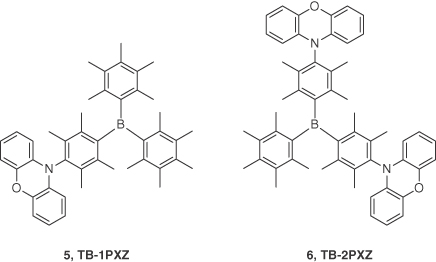
Figure 14.4 Chemical structures of emitters 5 and 6.
To achieve high efficiencies, TADF emitters are usually employed as dopants in a host material to prevent concentration quenching. The choice of host material becomes critical, especially for blue emitters since a wide bandgap material with high triplet energy is required. Solution processability of such materials further limits the choice of host materials available. To overcome this limitation, Sun et al. [30] reported a host and emitter design 7 (DV‐CDBP) and 8 (DV‐MOC‐DPS), respectively, with thermally cross‐linkable pendant units designed to improve the film‐forming capabilities of emissive layer. Compound 7 was chosen as the host because of its high triplet energy of 2.95 eV. Compound 8 exhibited a ΔEST of 0.31 eV but with a λPL of 430 nm and ΦPL of 71% in 9 wt% doped film of 8 in 7. The transient photoluminescence spectrum revealed a prompt emission decay, τp, of 11 ns and a τd of 50 μs in degassed toluene, a typical profile for a TADF emitter. A solution‐processed device using the device stack ITO/PEDOT:PSS (30 nm)/8 doped in 7 in the mass ratio 1 :0.09 (50 nm)/TPBI (40 nm)/Cs2CO3 (2 nm)/Al (100 nm) exhibited a maximum EQE of 2.0% (1.3% at 100 cd m−2) with current and power efficiencies of 1.6 cd A−1 and 0.9 lm W−1, respectively. A deep blue emission with λEL of 444 nm and CIE coordinates of (0.12, 0.13) was realized for the device. Although the efficiencies of the devices were below the 5% threshold to unequivocally demonstrate that triplet excitons are being harvested in the device, these materials do demonstrate a promising strategy to transform emitters designed for vacuum‐deposited OLEDs [54] into ones compatible for solution‐processed OLEDs.
As described at the beginning of this section, a deep blue emitter is defined by its CIE coordinates ranging from (0.14, 0.08) to (0.15, 0.06). The solution‐processed TADF OLED with CIE coordinates most closely approaching the blue standard so far is based on emitter 4, exhibiting an EQE of 20% but with CIE coordinates of (0.16, 0.25), which are still fairly far from the standard. The “bluest” solution‐processed OLED showed better CIE coordinates of (0.12, 0.13) using 8 as the emitter; however the maximum EQE for this device was considerably lower at 2%. Thus, the development of high‐performance deep blue TADF OLEDs remains a challenge for both solution‐processed and vacuum‐deposited devices (Figure 14.5).
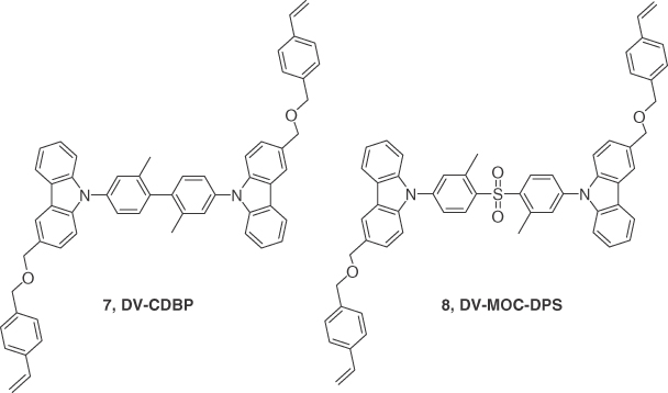
Figure 14.5 Chemical structures of emitters 7 and 8.
14.1.2 Solution‐Processed Green TADF Materials and Devices
The NTSC standard defines green color by CIE coordinates of (0.20, 0.71), and CIE coordinates of a pure green emission defined by the PAL standard are (0.29, 0.60). In this section, we have defined green emitters as those with λEL from 490 to 550 nm. Although a pure 490 nm emission would not be green, the broad emission spectrum of the organic semiconductors means that materials with emission peaking at 490 nm are typically closer to green than blue. The photophysical properties of emitters 9–17 and EL characteristics of the corresponding OLEDs are summarized in Tables 14.1 and 14.2, respectively.
The era of development of high‐efficiency green TADF OLEDs began in 2012 when Uoyama et al. [31] reported the emitter 2,4,5,6‐tetra(carbazol‐9‐yl)‐1,3‐dicyanobenzene (4CzIPN), 9. Compound 9 exhibited a λPL at 507 nm and a very high ΦPL of 94% in degassed toluene. The relatively short τd of 5.1 μs is indicative of TADF behavior, which was further confirmed by a small ΔEST of 83 meV. The device structure used was based on the following architecture: ITO/NPB (35 nm)/9: CBP (6 wt%, 15 nm)/TPBI (65 nm)/LiF (0.8 nm)/Al (100 nm). An EQE close to 19.3% was obtained with λEL at 520 nm for the OLED fabricated by vacuum deposition. This high device efficiency was comparable with those of highly efficient green phosphorescent OLEDs. Inspired by these results, Cho et al. [32] developed high‐efficiency solution‐processed OLEDs by modifying the structure of 9 with either methyl (10; m4CzIPN) or tert‐butyl (11; t4CzIPN) groups decorating the carbazole donors to improve the solubility of the materials. In their study, 9 displayed λPL at 507 nm in 1 wt% doped CzSi film, while the emission of 10 and 11 were redshifted by about 20 nm due to the inductively electron‐donating nature of the alkyl groups that strengthen the donor character. The ΦPL of 1 wt% doped films of 10 and 11 in CzSi were 67% and 78%, respectively, where CzSi serves as a high bandgap host, and were lower than that of 9 (ΦPL = 94%). Compounds 9–11 in 1 wt% CzSi spin‐coated films showed τd of 3.1, 2.6, and 2.9 μs, respectively. Uniform film morphology and efficient energy transfer from the host to the dopant translated to high‐performance solution‐processed devices with the following architecture: ITO/PEDOT:PSS (60 nm)/PVK (15 nm)/9, 10, 11: CzSi (1 wt%, 30 nm)/TSPO1 (35 nm)/LiF(1 nm)/Al(200 nm). Devices exhibited green emission with λEL of 520, 540, and 545 nm and CIE coordinates of (0.20, 0.43), (0.29, 0.57), and (0.31, 0.59) for 9, 10, and 11, respectively. The maximum EQE reported for these devices using 9–11 were of 8.1%, 8.2%, and 18.3%, which reduced to 7.2%, 5.4%, and 12.0% at a luminance of 1000 cd m−2, respectively (Figure 14.6).
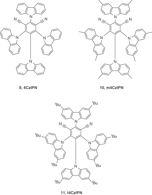
Figure 14.6 Chemical structures of emitters 9, 10, and 11.
Although the solution‐processed OLED using 9 reported by Cho et al. [32] did not perform close to its vacuum‐deposited analogue, a much improved OLED using 9 was realized later by Suzuki et al. [50] They developed a new host material, 1,3‐bis{3‐[3‐(9‐carbazolyl)phenyl]‐9‐carbazolyl}benzene (CPCB), possessing a high triplet energy of 2.79 eV, and compared the device performance using this bespoke host to that with CBP as the host. Conjugation length and high triplet energy were maintained by linking four carbazole units to three phenyl bridges via the metapositions. The host CPCB showed good solubility (>5 wt%) in many polar solvents, which are typically used in solution processing; 6 wt% doped films of 9 in CPCB exhibited a high ΦPL of 86% under nitrogen‐saturated conditions. A solution‐processed device based on the architecture ITO/PEDOT:PSS(40 nm)/9:CPCB 6 wt% (30 nm)/T2T(10 nm)/Bpy‐TP2(40 nm)/LiF(1 nm)/Al (100 nm) showed an EQE of 9.9% (9.8 at 1000 cd m−2). They also fabricated solution‐processed devices using CBP as the host with the same device structure and realized a slightly improved EQE of 11.9% (11.4% at 1000 cd m−2). Although devices doped in CPCB have lower efficiencies than their CBP‐based counterparts, nonetheless CPCB was proved to be an effective host material for solution‐processed TADF devices. Moreover, replacing the Bpy‐TP2 electron‐transporting layer (ETL) with TPBI resulted in a dramatic improvement of the EQE to 18.5% (17.2% at 1000 cd m−2), which is close to the 19.3% realized for the corresponding vacuum‐deposited OLED [31]. The improvement in efficiency was attributed to the increased quenching of excitons by the PEDOT:PSS layer due to its lower singlet energy (1.6 eV) in the case where Bpy‐TP2 was used as the ETL. On using T2T/Bpy‐TP2 as ETLs, the recombination zone in the EML was shifted toward (host/hole‐injection layer) HIL/EML interface (i.e. PEDOT:PSS/EML) due to improved electron transport in ETL and injection into the EML from T2T/Bpy‐TP2 layer.
After optimizing the device performance with 9 as the emitter by varying the host material, Komatsu et al. [51] fabricated solution‐processed devices and evaluated their performance as a function of ETL material. Specifically, a comparison of device performance was drawn using B3PyPB and B4PyMPM as ETL versus TPBI as ETL in devices with the following architecture: ITO/PEDOT:PSS (30 nm)/9:CBP (35 nm)/ETL (65 nm)/Liq (3 nm)/Al (100 nm), with 9 doped at 5 or 15 wt% in CBP. TPBI‐based OLEDs with doping concentration of 9 at 5 wt% showed a maximum EQE of 9.4% at a luminance of 1000 cd m−2, which varied little upon increasing the doping concentration to 15 wt% (maximum EQE = 9.9%; 9.3% at a luminance of 1000 cd m−2). Compound 9 has a deep ionization potential/electron affinity of 6.1/3.7 eV. Since TPBI has a shallow ionization potential of 6.3 eV, it does not have sufficient hole‐blocking ability and therefore efficiency suffers. To solve this problem, B3PyPB and B4PyMPM were used as ETL materials due to their deep HOMO levels of 6.6 eV [55] and 7.1 eV [56], respectively, and high electron mobility of ∼10−4 cm2 V−1 s−1. OLEDs with 5 wt% 9 in CBP and using B3PyPB or B4PYMPM showed much improved maximum EQEs of 15% (13% at 1000 cd m−2) and 16% (13% at 1000 cd m−2), respectively, due to more effective hole blocking by the ETL. These maximum EQEs are among the highest reported efficiencies for solution‐processed TADF devices and are not only close to highly efficient vacuum‐deposited green TADF materials but also comparable to the best solution‐processed green phosphorescent materials [20, 24b]. Further improvement in solution‐processed TADF green devices using 9 as the emitter was realized when Kim et al. [49] simplified the device structure by eliminating the PVK HTL (hole transporting layer). TADF devices without HTL can suffer from severe exciton quenching at the PEDOT:PSS/EML interface, which can limit the efficiency to a great extent. To overcome this problem, a self‐organized buffer hole‐injection layer (Buf‐HIL) was employed consisting of PEDOT:PSS and tetrafluoroethylene‐perfluoro‐3,6‐dioxa‐4‐methyl‐7‐octene‐sulfonic acid copolymer (PFI) [57]. The lower surface energy of PFI resulted in its rise to the top surface during spin‐coating of Buf‐HIL. This process led to the formation of a self‐organized Buf‐HIL with gradient PFI concentration, [PFI], which increased gradually from bottom to top of the HIL. Due to the deep ionization potential of PFI, this gradient [PFI] resulted in a gradual increase of the work function (WF) of Buf‐HIL from 5.20 eV at the bottom to 5.95 eV at the top surface of the HIL. This gradual increase in WF facilitated the hole injection from ITO to the bottom surface and hole transporting to the host from the top surface. CBP was chosen as the host as a good match of the Buf‐HIL WF with the HOMO (6.0 eV) of CBP. This not only improved the hole/electron balance in the EML but also avoided exciton quenching at the interface of the HIL/EML by eliminating the accumulation of holes at that interface. Solution‐processed devices (ITO/Buf‐HIL (40 nm)/9: CBP (40 nm)/ TPBI(50 nm)/ LiF(1 nm)/ Al(100 nm)) attained a maximum EQE of 24%, PE of 58 lm W−1, which were much greater than the PEDOT:PSS‐based OLEDs (maximum EQE = 15%, PE = 17.5 lm W−1) and the vacuum‐deposited OLEDs (maximum EQE = 19.3%). This device is the most efficient reported to date for a solution‐processed OLED employing a pure organic TADF emitter.
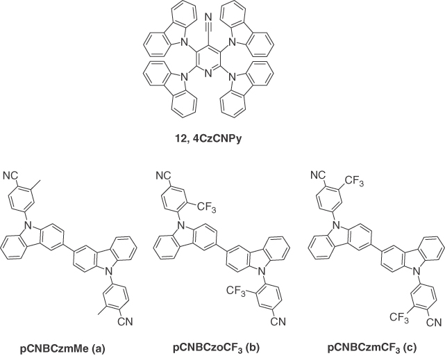
Figure 14.7 Chemical structures of emitter 12 and host materials a–c.
Inspired by the structure of 9, Tang et al. [33] employed a related acceptor in 4‐cyanopyridine, producing the emitter 2,3,5,6‐tetracarbazolyl‐4‐cyano‐pyridine (4CzCNPy), 12, and simultaneously developed a cyano‐free new host material 4CzPy. Compound 12 showed strong green‐yellow emission with λPL at 536 nm in chloroform solution and a yellow emission (λPL = 560 nm) in 8 wt% doped in 4CZPy thin film. The ΦPL of the film was 24.7% under ambient conditions, which increased to 54.7% under oxygen‐free conditions. A τd of 8.4 μs and ΔEST of 0.07 eV confirmed the TADF nature of the emission. By using 12 as the dopant in either the high triplet energy 4CZPy (2.8 eV) or mCP as hosts in a simple three layer solution‐processed device of ITO/PEDOT:PSS (40 nm)/12:host (8 wt%, 30 nm)/TmPyPB (60 nm)/LiF (1 nm)/Al (100 nm), maximum EQEs of 10.4% (9.6% at 1000 cd m−2) and 11.3% (10.6% at 1000 cd m−2) were achieved, respectively, with λEL of 524 nm and CIE coordinates of (0.35, 0.59) obtained for both the devices. A maximum luminance of 21 431 cd m−2 and current density of 273 mA cm−2 were obtained at an operational voltage of 13.9 V using 4CZPy as the host. On the other hand, these values were 16 305 cd m−2, 225 mA cm−2, and 14.4 V for mCP‐based devices. The low cost, high luminance, and high efficiency demonstrated the promise of emitter 12 in EL devices. To further study the effect of the host material on the device performance, the same group developed three new hybrid TADF host materials based on alkyl‐substituted bicarbazole/cyanobenzene [52]. Three simple bicarbazole derivatives, namely, pCNBCzmMe (a), pCNBCzoCF3 (b), and pCNBCzmCF3 (c), were synthesized by decorating the 9‐positions of bicarbazole with cyanobenzene to improve the solubility and electron‐transporting capabilities of the materials, while methyl and trifluoromethyl moieties were introduced to fine‐tune their optoelectronic properties. The chemical structures of these three host materials are shown in Figure 14.7, and the data collected in Table 14.3. These three materials exhibited TADF properties with ΔEST of 0.30, 0.19, and 0.14 eV for a–c, respectively, in pristine neat films. They fabricated solution‐processed devices for double TADF host/dopant system using these three TADF materials as host and 12 as TADF dopant with the configuration of ITO/PEDOT:PSS(40 nm)/12:Host (8 wt%, 40 nm)/TmPyPB (60 nm)/LiF (1 nm)/Al (100 nm). A maximum brightness >14 000 cd m−2 and EQEs ranging from 10% to 11% that remained almost identical at a luminance of 100 cd m−2 were achieved containing these hosts. Although devices with double TADF host–guest system did not much improve the EQE of the OLED with 12, it did reveal an interesting approach of designing host–guest systems that may improve charge transport.
Table 14.3 Chemical structures of host, hole transporting, and electron‐transporting materials.
| Material | Structure | Type |
| PEDOT:PSS |  |
Hole transporting layer (HTL) |
| PVK |  |
Host/hole‐injection layer (HIL) |
| mCP | 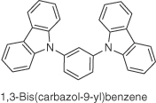 |
Host |
| CzSi |  |
Host |
| CBP |  |
Host |
| DV‐CDBP | ![Chemical structure of 9,9′-(2,2′-dimethyl-[1,1′-biphenyl]-4,4′-diyl)bis(3-(((4-vinylbenzyl)oxy)methyl)-9H-carbazole) (DV-CDBP).](http://images-20200215.ebookreading.net/4/1/1/9783527339006/9783527339006__highly-efficient-oleds__9783527339006__images__c14t003f.jpg) |
Host |
| CPCB |  |
Host |
| 4CZPy |  |
Host |
| pCNBCzmMe | ![Chemical structure of 4,4′-(9H,9′H-[3,3′-bicarbazole]-9,9′-diyl)bis(2-methylbenzonitrile) (pCNBCzmMe).](http://images-20200215.ebookreading.net/4/1/1/9783527339006/9783527339006__highly-efficient-oleds__9783527339006__images__c14t003i.jpg) |
Host |
| pCNCZoCF3 | ![Chemical structure of 4,4′-(9H,9′H-[3,3′-bicarbazole]-9,9′-diyl)bis(2-methylbenzonitrile) (pCNCZoCF3).](http://images-20200215.ebookreading.net/4/1/1/9783527339006/9783527339006__highly-efficient-oleds__9783527339006__images__c14t003j.jpg) |
Host |
| pCNCZmCF3 | ![Chemical structure of 4,4′-(9H,9′H-[3,3′-bicarbazole]-9,9′-diyl)bis(2-(trifluoromethyl)benzonitrile) (pCNCZmCF3).](http://images-20200215.ebookreading.net/4/1/1/9783527339006/9783527339006__highly-efficient-oleds__9783527339006__images__c14t003k.jpg) |
Host |
| PBD |  |
Host |
| TAPC |  |
Host |
| TCTA |  |
Host |
| TPBI |  |
Electron‐transporting layer (ETL) |
| TmPyPB | ![Chemical structure of 1,3,5-Tri[(3-pyridyl)-phen-3-yl]benzene (TmPyPB).](http://images-20200215.ebookreading.net/4/1/1/9783527339006/9783527339006__highly-efficient-oleds__9783527339006__images__c14t003p.jpg) |
Electron transporting layer (ETL) |
| TSPO1 |  |
Hole‐blocking layer (HBL) |
| T2T | ![Chemical structure of 2,4,6-tri([1,1′-biphenyl]-3-yl)-1,3,5-triazine (T2T).](http://images-20200215.ebookreading.net/4/1/1/9783527339006/9783527339006__highly-efficient-oleds__9783527339006__images__c14t003r.jpg) |
Hole‐blocking layer (HBL) |
| Bpy‐TP2 | ![Chemical structure of 2,7-di([2,2′-bipyridin]-5-yl)triphenylene (Bpy-TP2).](http://images-20200215.ebookreading.net/4/1/1/9783527339006/9783527339006__highly-efficient-oleds__9783527339006__images__c14t003s.jpg) |
Electron‐transporting layer (ETL) |
| B3PyPB |  |
Electron‐transporting layer (ETL) |
| B3PyMPM |  |
Electron‐transporting layer (ETL) |
| B4PyMPM | 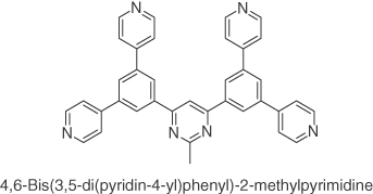 |
Electron‐transporting layer (ETL) |
PEDOT and PSS, Poly(3,4‐ethylenedioxythiophene)polystyrene sulfonate.
A distinct approach of using charged emitters in nondoped solution‐processed TADF OLEDs was first reported by our group [34]. We developed a charged emitter 13 by tethering methylimidazolium units onto 2CzPN [31]. The ΦPL of 13 was 73% doped in 10 wt% PMMA film under ambient conditions, which increased to 90% under nitrogen‐saturated conditions. The τd of 6.34 μs confirmed its TADF nature. Solution‐processed OLEDs using the device structure of ITO/PEDOT:PSS(30 nm)/PVK(30 nm)/13:mCP:OXD7 or neat 13 (10 wt%, 30 nm)/B3PyMPM(60 nm)/Ca(20 nm)/Al(100 nm) were fabricated using a double host system with mCP and OXD7 to balance and confine the hole ratio in the EML. The device with neat 13 as the EML produced a green OLED with λEL = 546 nm and CIE coordinates of (0.41, 0.53) with a maximum EQE of 5.1% with low turn‐on voltage of 3.6 V, which outperformed the device with the doped EML (maximum EQE = 2.7%, turn‐on voltage of 5.8 V). Although the neat‐film device did not exceed the previous reported EQEs of green solution‐processed OLEDs, its performance metrics were still superior to the few reports of nondoped TADF OLEDs in the literature [26, 38] (Figure 14.8).

Figure 14.8 Chemical structure of emitter 13.
So far, most of the research have focused on developing and modifying the D–A materials that are mainly based on carbazole as the donor. A handful of reports of vacuum‐deposited highly efficient TADF emitters exist in the literature where disubstituted acridan units are used as donors [36]. Acridan was first employed as a donor in a solution‐processable TADF emitter 3ACR‐TRZ, 14, which contains a triazine acceptor unit [35]. They doped 16 wt% 14 into CBP, which resulted in an emission with λPL at 504 nm with an outstanding ΦPL of 98% under nitrogen‐saturated atmosphere. The τd was measured to be 6.7 μs, while a ΔEST of only 15 meV confirmed the TADF nature of the emitter. Solution‐processed OLEDs based on the device structure ITO/PEDOT:PSS (35 nm)/16 wt% 14:CBP (55 nm)/B3PyPB (30 nm)/Liq (1 nm)/Al(100 nm) were fabricated. The OLEDs produced blue‐green emission with λEL = 504 nm, a maximum EQE of 18.6% and a power efficiency of 36.3 lm W−1. Motivated by the excellent device performance of 14, Wada et al. [53] developed emitter DMAC‐TRZ, 15, based on the same electron donor and acceptor fragments as 14 and reported a maximum EQE of 20% by vacuum depositing a host‐free neat film of 15. These encouraging results led the same group to fabricate a solution‐processed device with 15 as the emitter [53]. A neat film of 15 prepared by spin‐coating showed a ΦPL of 84% that was almost identical to that found for its vacuum‐deposited film (ΦPL = 83%). Solution‐processed devices based on ITO/PEDOT:PSS (40 nm)/15 (30 nm)/BmPyPB (60 nm)/Liq (1 nm)/Al (100 nm) exhibited a maximum EQE of 17.5% with λEL of 498 nm, which was not only comparable to the nondoped vacuum‐deposited counterpart (maximum EQE = 20%) but is also the highest value reported to date for a nondoped TADF solution‐processed OLED (Figure 14.9).
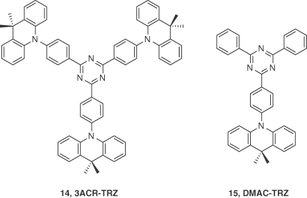
Figure 14.9 Chemical structures of emitters 14 and 15.
After employing acridan to develop green high‐performance TADF emitters, Liu et al. [29] reported solution‐processed TADF emitters based on phenoxazine as donor units. They developed a series of triarylborane‐based TADF emitters, namely, TB‐1PXZ (5), TB‐2PXZ (6), and TB‐3PXZ (16) by varying the number of donor units and studied their optoelectronic properties. Emitters 5 and 6 produce blue light and were discussed in the previous section. Compound 16 showed a λPL at 509 nm with a near‐unity ΦPL 95% in 10 wt% doped CzSi films under nitrogen‐saturated conditions. A barely resolved ΔEST of 0.01 eV and a very short τd of 1.3 μs confirmed its TADF nature. Solution‐processed devices based on ITO/PEDOT:PSS (30 nm)/16:CzSi: (10 wt%, 40 nm)/TmPyPB(40 nm)/Liq (2 nm)/Al (100 nm) exhibited a maximum EQE of 13.6% (12.3% at luminance of 100 cd m−2) with an λEL of 510 nm and CIE coordinates of (0.23, 0.54). The high efficiency observed for the OLED with 16 was attributed to its high ΦPL and efficient rISC process due to the very small ΔEST (Figure 14.10).

Figure 14.10 Chemical structure of emitter 16.
To further enhance the device performance, another TADF emitter 17 (ACRDSO2) was reported by Xie et al. [37] In their design a novel acceptor, thianthrene‐9,9′,10,10′‐tetraoxide, was coupled to a dimethylacridan, DMAC, donor through a phenyl bridge. Compound 17 exhibited a λPL at 520 nm with ΦPL of 71% in 6 wt% doped CBP films. Moreover, a ΔEST of 0.058 eV and a short τd of 8.3 μs are indications of efficient rISC. Solution‐processed devices with the device structure ITO/Buf‐HIL (40 nm)/6 wt% 17:CBP (35 nm)/TmPyPB (55 nm)/LiF (1 nm)/Al (100 nm) showed a maximum EQE of 17.5% at a luminance of 100 cd m−2 with an λEL at 534 nm (Figure 14.11).
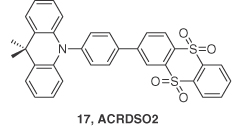
Figure 14.11 Chemical structure of emitter 17.
14.1.3 Solution‐Processed Yellow‐to‐Red TADF Materials and Devices
NTSC standard defines red color by CIE coordinates of (0.67, 0.33), and CIE coordinates of a pure red emission defined by PAL standard are (0.64, 0.33). In this section, we have defined the yellow‐to‐red emitters as those whose λEL lie between 550 nm and 644 nm. The photophysical properties of 18–20 and the EL characteristics of corresponding OLEDs are summarized in Tables 14.1 and 14.2, respectively.
Far less effort has been devoted to the design of efficient long wavelength TADF emitters compared with the focus on blue and green emitters. Due to a trade‐off between singlet–triplet energy splitting and high fluorescence radiative rates [58], it is difficult to design and realize highly efficient TADF emitters, especially orange/red emitters, which tend to exhibit low ΦPL values because nonradiative decay rates increase exponentially with the emission wavelength following the well‐known energy gap law [59]. Uoyama et al. [31] reported an orange emitter 4CzTPN where the vacuum‐deposited OLED produced orange light with a λEL of 585 nm in EL and maximum EQE of 11.2%. In order to improve the efficiency of red‐emitting devices, the same group developed emitters employing a central anthraquinone acceptor and two donors separated by a phenyl bridge from the acceptor. The introduction of the bridge was designed to enhance the radiative decay rates. Employing emitters d–f (Figure 14.12) in OLEDs led to devices with EQEs of 12.5%, 9.0%, and 6.9%, respectively, with corresponding λEL values of 624, 637 and 584 nm, respectively [60]. These efficiencies are among the highest reported to date for vacuum‐deposited red TADF OLEDs.
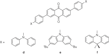
Figure 14.12 Chemical structures of emitters d–f.
To realize solution‐processed red TADF OLEDs, Chen et al. [38] reported a dithienylbenzothiadiazole‐based TADF emitter, 18 (red‐1b), which exhibited λPL at 644 nm in neat film with a ΦPL of 28% under nitrogen‐saturated conditions. The ΔEST of 0.40 eV is unusually large for a TADF material, and the short τd of 828 ns is probably reflective of increased nonradiative decay. A solution‐processed nondoped device based on ITO/PEDOT:PSS (35 nm)/PVK (30 nm)/18 (30 nm)/TPBI (60 nm)/CsF(1 nm)/Al (100 nm) realized a maximum EQE of 1.75% (1.27% at a luminance of 100 cd m−2) with pure red emission (λEL = 644 nm). The authors explained and confirmed the delayed fluorescence in the EL device by performing magneto‐electroluminescence (MEL) measurements and attributed the emission mechanism to the coexistence of TADF and TTA. MEL is a tool to study rISC and TTA by the relative variation of EL intensity versus the strength of an external magnetic field. For an emitter showing prompt and delayed fluorescence, prompt fluorescence is a magnetic field independent because the direct radiative decay of the singlets is not affected by magnetic field. In the absence of an external magnetic field, rISC is very efficient between three degenerate triplet substates (T−1, T0, and T+1) and the singlet state (S1). In the presence of a strong external magnetic field, Zeeman splitting of the triplet states lifts the degeneracy between T−1 and T+1 states, leaving only one channel for rISC from T0 to S; partly blocking the rISC and as a result leading to a decreased TADF. The MEL of emitter 18 consisted of a rapid decrease in the presence of external magnetic field (Figure 14.13).
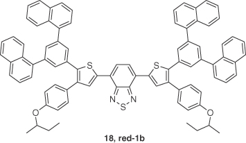
Figure 14.13 Chemical structure of emitter 18.
To overcome the existing limited EQE observed for red TADF OLEDs, Yu et al. [39] reported an asymmetric D–A TADF molecule (FDQPXZ), 19 containing fluorine‐substituted quinoxaline acceptor and phenoxazine donor units. Fluorine was introduced to increase the acceptor strength and redshift the emission further. Compound 19 showed a very small ΔEST of 0.04 eV, favorable for efficient rISC with a λPL of 606 nm in 5 wt% doped Bepp2 films with a ΦPL of 74%. The prompt and delayed lifetimes are 29 ns and 3.2 μs, respectively, demonstrating the TADF nature of the emission. Solution‐processed devices based on ITO/PEDOT:PSS(40 nm)/10 wt% 19:CBP:PBD (40 nm)/TmPyPB (50 nm)/LiF (1 nm)/Al (100 nm) exhibited a maximum EQE of 9.0% (7.8% at a luminance of 100 cd m−2) with a λEL of 600 nm and CIE coordinates of (0.53, 0.46), which was the first example of a high‐performance solution‐processed orange‐red TADF OLED (Figure 14.14).
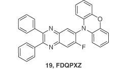
Figure 14.14 Chemical structure of emitter 19.
To further enhance the device performance, red TADF emitter 20 was reported by Xie et al. [37] They developed a novel acceptor thianthrene‐9,9′,10,10′‐tetraoxide and coupled it with phenoxazine (20; PXZDSO2). In many TADF emitter designs effective separation between the HOMO and LUMO, and hence, small ΔEST is achieved as a result of a large torsional angle between donor and acceptor. However, an overly large dihedral angle prevents efficient radiative decay from S1 to S0 by reducing the transition dipole moment according to Fermi's golden rule [61]. Thus, the introduction of the phenyl spacer group was designed to weaken the nonradiative internal conversion by elongating the distance between donor and acceptor moieties, and hence, to increase the ΦPL while maintaining a small ΔEST. Compound 20 exhibited λPL at 540 nm with ΦPL of 62% in 6 wt% doped CBP films. A ΔEST of 48 meV and a short τd of 5.0 μs for 20 favored an efficient rISC. Solution‐processed devices with the device structure ITO/Buf‐HIL (40 nm)/6 wt% 20:CBP (35 nm)/TmPyPB (55 nm)/LiF (1 nm)/Al (100 nm) showed a maximum EQE 15.2% at a luminance of 100 cd m−2 for 20. The OLED with 20 exhibited yellow emission with λEL at 552 nm and CIE coordinates of (0.42, 0.55). The OLED with the yellow emitter 20 proved to be the first example of a solution‐processed device that exhibited a comparable performance with a vacuum‐deposited OLED of the same approximate energy (Figure 14.15).

Figure 14.15 Chemical structures of emitter 20.
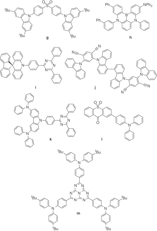
Figure 14.16 Chemical structures of emitters g–m.
14.1.4 Comparison of State‐of‐the‐Art Solution‐Processed OLEDs to Vacuum‐Deposited Counterparts
To further optimize the device performance of solution‐processed TADF OLEDs, it is crucial to understand the performance difference between state‐of‐the‐art OLEDs fabricated by solution processing and vacuum deposition. Since the first report of solution‐processed TADF OLEDs in 2014, this field has progressed remarkably, and EQEs comparable to state‐of‐the‐art vacuum‐deposited TADF OLEDs have already been achieved for each of blue, green, and red colors. Achieving a deep blue emission yet maintaining high efficiency is quite challenging. The deepest blue vacuum‐deposited TADF emitter reported to date is based on a sulfone acceptor and tert‐butylcarbazole donor (emitter g, Figure 14.16) moieties and possessed an EQE of 9.9% (λEL 423 nm) while exhibiting impressive CIE coordinates of (0.15, 0.07) [54]. A redshift in the EL spectrum usually accompanies a more efficient OLED in the blue. For example, the OLED with emitter h has a λEL of 468 nm yet retains deep blue CIE coordinates of (0.12, 0.13) along with an EQE of 20.2% [62]. A further shift in λEL to 490 nm for emitter i coincided with an impressive maximum EQE of 36.7% (35% at 100 cd m−2) emitting with CIE coordinates of (0.18, 0.43) [63]. In fact, this device remains the most efficient reported for small molecule‐based TADF OLEDs to date. By comparison, the best solution‐processed TADF blue OLED in terms of maximum EQE reported thus far is based on emitter 4 with the OLED exhibiting a maximum EQE of 20% with CIE coordinates of (0.16, 0.25). Vacuum‐deposited TADF OLEDs based on emitter j showed an EQE of 19.5% with CIE coordinates (0.16, 0.23); almost identical in emission color to solution‐processed TADF OLED of emitter 4 [64]. From this comparison, there is still room for improved solution‐processed blue TADF OLEDs. For the green OLEDs, the most efficient vacuum‐deposited device is based on emitter k and exhibited maximum EQE of 29.6% (26% at 100 cd m−2) with λEL at 520 nm [65]. Solution‐processed devices provide comparable performance with the most efficient based on emitter 9 showing an EQE of 24% with an identical EL emission maximum and CIE at (0.20, 0.43). When it comes to the comparison of OLEDs emitting at lower energy, EQEs of 15.2% and 9.0% have been achieved for emitters 20 and 19 with λEL of 552 and 600 nm, respectively, for solution‐processed devices, whereas for the most efficient vacuum‐deposited OLEDs, these values are higher at 18.5% for yellow with λEL at 552 nm (emitter l) [66] and 17.5% for red with λEL at 610 nm (emitter m) [67].
14.1.5 Solution‐Processed TADF Polymers and Dendrimers
We have so far only discussed the transfer of TADF technology from vacuum‐deposited OLEDs to solution‐processed OLEDs using small molecule TADF emitters and hosts. In the solution processing of small molecules, the tactic is to blend these functionalized small molecule TADF dopants into various hosts in order to maintain good charge transport and film morphology characteristics. However, the host–guest blend approach has significant challenges including dopant aggregation, diffusion of dopants into the clusters of hosts and into neighboring layers, and the propensity for the dopant to form microcrystalline domains, leading to poor film morphology [68]. Polymers, on the other hand, are particularly suitable for solution processing to make high quality films, e.g. by spin‐coating or blade‐coating. Furthermore the viscosity of polymer solutions can be readily adjusted to be ideal for inkjet printing. Light‐emitting dendrimers have also proved a very effective strategy for conferring solution processability and controlling aggregation [13, 20, 69]. However, it is not trivial to achieve TADF in polymers and dendrimers given the challenge of simultaneously achieving small ΔEST and suppression of internal conversion in molecules containing many atoms. Additionally, intermolecular and intramolecular TTA quenches the triplet populations in polymers easily. Despite these challenges, TADF polymers and dendrimers would be attractive materials for solution‐processed OLEDs. To date through, there have only been a handful of reports of TADF polymers and dendrimers. In this section we discuss these materials (emitters 21–40) in terms of their photophysical properties and EL characteristics of the corresponding OLEDs (Tables 14.1 and 14.2, respectively).
Keeping the design strategies of TADF in mind, π‐conjugated polymers have been utilized in realizing solution‐processed TADF OLEDs. Nikolaenko et al. [40] reported the first example of a TADF polymer based on a strategy, which they called “intermonomer TADF.” They proposed an approach where donor and acceptor centers were distinct monomers, which upon polymerization, formed the charge transfer (CT) emitter. The polymer, 21, exhibited a small ΔEST due to the spatial separation of HOMO and LUMO, enabling efficient thermal upconversion of triplet excitons (Figure 14.17). They used a bis(diarylamine) donor and a 1,3,5‐triazine acceptor as monomers and added a high T1 energy backbone monomer 1,4‐bis(4‐(4,4,5,5‐tetramethyl‐1,3,2‐dioxaborolan‐2‐yl)phenyl)butane to break the conjugation to avoid the TTA in polymeric structure. The optoelectronic characterization of the neat film of 21 revealed TADF character with the transient PL decay consisting of two components: prompt (15–50 ns) and delayed (1 μs to 50 ms), the ΦPL in air of 41% increasing slightly to 44% under nitrogen‐saturated conditions, and a ΔEST of 220 meV, determined from the peak position of the fluorescence and phosphorescence spectra. Polymer OLEDs were fabricated using device structure ITO/PEDOT:PSS (65 nm)/interlayer (40 nm)/21 (80 nm)/NaF (2 nm)/Al (100 nm)/Ag (100 nm). They used a polymeric interlayer (poly(2,5‐dihexylbenzene‐N‐(4‐(2‐butyl)phenyl)‐diphenylamine)) possessing a reasonably high triplet level (T1 = 2.52 eV) to minimize the triplet quenching in the TADF emissive layer and to prevent the aggregation of the TADF emissive cores. Devices showed a green emission with λEL at 530 nm and a maximum EQE of 10%.
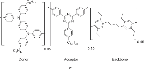
Figure 14.17 Chemical structure of emitters 21.
Luo et al. [41] prepared a series of copolymers (P0–P12) using a known TADF chromophore (PXZ‐OXD) [70] unit tethered to a poly(carbazole) backbone. The best device employed P12 (22). Polymer 22 exhibited a λPL at 494 nm with a ΦPL of 34% under nitrogen‐saturated conditions and a τd of 2.36 μs as a neat thin film. The solution‐processed OLED with the architecture (ITO/PEDOT:PSS (30 nm)/poly‐TPD (40 nm)/neat 22 (50 nm)/TmPyPB (35 nm)/Ba (20 nm)/Al (100 nm)) showed a maximum EQE of 4.3% (2.4% at luminance of 100 cd m−2) with λEL at 506 nm (Figure 14.18).
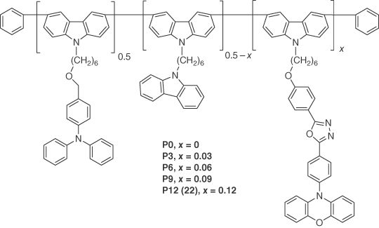
Figure 14.18 Chemical structure of emitter 22.
Using a similar strategy to that of Nikolaenko et al. Lee et al. [42] developed a class of π‐conjugated polymers 23 (pCzBP) and 24 (pAcBP) based on alternating benzophenone acceptor and carbazole/acridan donor cores. A 10 wt% doped blend film of these polymer in a mixed host matrix (TCTA:TAPC(65 : 25)) showed λPL at 508 and 540 nm with ΦPL of 23 and 46% under nitrogen‐saturated conditions for 23 and 24, respectively. Transient PL decays of 23 and 24 exhibited both prompt and delayed components where τd = 74 and 10 μs, respectively. The ΔEST extracted from the onset wavelengths of the doped film emission spectra at 300 and 5 K were exceedingly small at 16 and 4 meV for 23 and 24, respectively. OLED devices with the structure of ITO/PEDOT:PSS (40 nm)/23, 24:TCTA:TAPC (10 : 65 : 25, 40 nm)/TmPyPB (40 nm)/LiF (0.8 nm)/Al (80 nm) showed green emission for 23 and yellow emission for 24. The device using 23 achieved an EQE of 8.1% with λEL of 500 nm, while that of 24 showed an EQE of 9.3% with λEL of 548 nm; EQE of 24 remained as high as 8.1% at a luminance of 1000 cd m−2. These devices greatly exceeded the theoretical limit for conventional fluorescent OLEDs and provided a molecular design strategy for the further development of solution‐processed TADF polymer OLEDs (Figure 14.19).
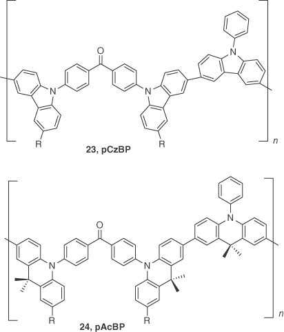
Figure 14.19 Chemical structure of emitters 23 and 24.

Figure 14.20 Chemical structure of emitters 25 and 26.
Zhu et al. [43] proposed an alternative strategy, exemplified in polymers 25 (PAPCC) and 26 (PAPTC), wherein the donor units are contained within the polymer backbone and the acceptor units grafted as the side chains (Figure 14.20). Pristine thin films of 25 and 26 displayed a broad, structureless emission with λPL at 472 and 510 nm and ΦPL of 9% and 44%, respectively, under nitrogen‐saturated conditions. Polymers 25 and 26 exhibited ΔEST of 0.37 and 0.13 eV, respectively, with very short τd of 0.32 and 0.23 μs, respectively. Solution‐processed devices based on ITO/PEDOT:PSS (50 nm)/neat 25 or 26 (40 nm)/TmPyPB (50 nm)/LiF (1 nm)/Al(100 nm) were fabricated and showed EQEs of 1.3% at a luminance of 6 cd m−2 with a λEL of 508 nm and 12.3% at a luminance of 180 cd m−2 with a λEL of 521 nm, respectively. The relatively high EQE for the device with 26 was attributed to its smaller ΔEST of 0.13 eV, which facilitated the effective upconversion of triplet excitons.
Employing similar strategies as those illustrated previously, a variety of highly efficient polymers 27–31 based on phenothiazine donors and a dibenzothiophene‐S,S‐dioxide acceptors were reported jointly by the groups of Bryce and coworkers [44]. Polymer 27 contained the phenothiazine donor in the backbone along with dibenzothiophene, whereas, a polystyrene (PS) backbone was used as a spacer dispersing unit in polymers 28–31 to suppress the internal conversion and TTA. Polymers 28–30 comprised of different molecular ratios of donor–acceptor with respect to styrene units. All the polymers showed broad and featureless emission spectra as pristine thin films with emission maxima ranging from 535 (28) to 556 nm (31). Characteristic PL decay kinetics were observed with τd ranging from 1 to 100 μs. ΔEST values for 27–31 were calculated to be 0.28, 0.35, 0.46, 0.42, and 0.40 eV, respectively. Solution‐processed polymer OLEDs were fabricated using the device structures ITO/PEDOT:PSS (40 nm)/27:PBD:PVK (10 : 40 : 50, 45 nm)/TPBI (50 nm)/LiF (1 nm)/Al (100 nm) and ITO/PEDOT:PSS (40 nm)/28–31:mCP (10 wt%, 45 nm)/TPBI (50 nm)/LiF (1 nm)/Al (100 nm) and showed maximum EQEs of 11.5% at a luminance of 1000 cd m−2 (λEL = 512 nm), 20.1% (λEL = 533 nm, EQE at 100 cd m−2 = 5.3%), 15.2% (λEL = 536 nm, EQE at 100 cd m−2 = 2.8%), 1.8% (λEL = 539 nm, EQE at 100 cd m−2 = 1.8%), and 1.4% (λEL = 556 nm, EQE at 100 cd m−2 = 0.6%) for 27–31, respectively. A sharp drop in EQE was observed with decreasing styrene content in the family 28–31 owing to the corresponding increase in TTA. A device of 28 was also fabricated using CBP as a host, and an EQE of 2.5% was achieved, while the EQE of the device with 28 using mCP as the host was much higher at 20.1%, demonstrating the importance of the host materials to the device performance (Figure 14.21).
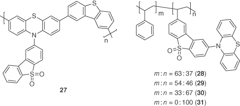
Figure 14.21 Chemical structures of emitters 27–31.
Recently, Xie et al. [45] reported a series of copolymers incorporating the TADF emitter 10‐(4‐((4‐(9H‐carbazol‐9‐yl)phenyl)‐sulfonyl)phenyl)‐10H‐phenoxazine (PCzDP). They synthesized four copolymers comprised of different molar ratios of PCzDP along with carbazole comonomers (32, Figure 14.22). In deaerated toluene solution, PCzDP‐5 (i.e. 5 mol% of PCzDP incorporated in the polymer) showed emission from both the backbone carbazole moiety (λPL = ∼425 nm) and PCzDP (λPL = ∼510 nm) with a ФPL of 50%, which clearly indicated that the concentration of PCzDP was insufficient for complete energy transfer from the comonomer. Polymers with higher concentrations of PCzDP (PCzDP‐10, PCzDP‐15, and PCzDP‐20) showed much less emission from the carbazole backbone and higher ФPL (67%, 66%, and 60%, respectively). On the other hand, in neat films all displayed emission solely from PCzDP (λPL = 497–509 nm) due to the presence of both intrachain and interchain energy transfer as a function of the greater packing density of the polymer in the solid state. PCzDP‐5 neat film had the lowest ФPL of 39%, whereas PCzDP‐10, PCzDP‐15, and PCzDP‐20 showed higher values (ФPL = 74%, 70%, and 59%, respectively). The TADF nature of the polymers was confirmed by the presence of a delayed fluorescence with very similar emission lifetimes (τd = 1.9–2.3 μs). The best device (ITO/PEDOT:PSS (50 nm)/PCzDP‐10 (70 nm)/TmPyPB (40 nm)/Liq (1 nm)/Al (100 nm)) showed a bluish‐green emission with λEL and CIE at 496 nm and (0.24, 0.40), respectively. The maximum EQE achieved was 16.1%, which dropped to 11.3% at a brightness of 100 cd m−2.
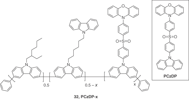
Figure 14.22 Chemical structure of emitter 32 (x = 5, 10, 15, or 20). Also shown in the inset is the reference TADF emitter (PCzDP).
Wei et al. [46] very recently demonstrated how a non‐TADF monomer (Figure 14.23) can be turned into a TADF macromolecule (macrocycle or polymer 33). In the monomer, the dihedral angle between the donor and the acceptor is as small as 50.6o, and hence a large ΔEST of 0.37 eV results. However, though this same dihedral angle is 50.7o in both the polymer and macrocycle, each has a much higher HOMO level of −5.14 eV compared with −5.59 eV for the monomer and hence the CT character of the excited state is greatly enhanced, which results in a significantly smaller ΔEST of 0.12 eV. Compound 33 (both polymer and macrocycle) exhibited a λPL of 496 nm, ΦPL of 71% with a τd of 296 μs in 2 wt% doped film of 33 in a PS host matrix, confirming its TADF character. This is the first report of turning on TADF activity by polymerization of a TADF‐inactive monomer. However, no device data are reported.

Figure 14.23 Chemical structures of A TADF‐inactive monomer (left) that can be transformed to be TADF‐active macrocycle or polymer (33).
Source: Ref. [51]. Reproduced with permission of Elsevier.
The previous examples of solution‐processed TADF OLEDs based on both small molecules and polymers demonstrate the potential of this family of devices. Another class of solution‐processable materials are dendrimers, and phosphorescent dendrimers have been widely explored as efficient solution‐processable OLED materials [13, 71] but only recently has attention turned to adapting this class of compounds into TADF emitters.
Albrecht et al. [26] reported the first example of a TADF dendrimer and its use in a nondoped, solution‐processed OLED. They developed three carbazole dendrimer generations with a triazine core (34 (G2TAZ), 35 (G3TAZ), and 36 (G4TAZ)). All three dendrons showed almost identical pristine thin film emission spectra with λPL at 500 nm. Compounds 34–36 exhibited miniscule ΔEST of 0.03, 0.06, and 0.06 eV, respectively, with ΦPL of 52%, 31%, and 8.4% under nitrogen‐saturated conditions. Their τd were measured to be 3.1, 1.9, and 2.4 μs for 34, 35, and 36, respectively. Nondoped solution‐processed devices were fabricated with the structure ITO/PEDOT:PSS (30 nm)/34, 35, and 36 (35 nm)/TPBI (40 nm)/Ca (10 nm)/Al(100 nm). Maximum EQEs reached 2.4% (λEL = 510 nm), 3.4% (λEL = 500 nm), and 1.5% (λEL = 498 nm) for 34–36, respectively. These efficiencies were higher than the EQEs expected assuming that only singlet emission was contributing to the EL emission. Although the EQEs were less than 5%, this report nevertheless demonstrated the utility of employing dendrimers in solution‐processable, nondoped OLED devices (Figure 14.24).
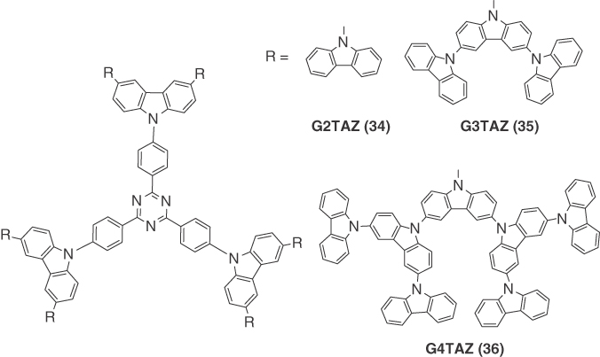
Figure 14.24 Chemical structure of emitters 34, 35, and 36.
To achieve high EQE in dendrimer‐based OLEDs, Li et al. [47] developed two TADF dendrons, 37 (CDE1) and 38 (CDE2). These dendrons were based on a TADF emissive core, DMAC–BP [72], which was previously shown to be an excellent TADF emitter with a high ΦPL of 85% in thin film. They revealed that these dendrimer‐based OLEDs showed a dual channel emissive feature where both TADF and interfacial exciplex emission were observed. Compounds 37 (λPL = 520 nm) and 38 (λPL = 499 nm) showed a blueshifted emission in neat film compared with DMAC‐BP (λPL = 506 nm), suggesting that the appended dendrons completely suppressed the intermolecular interactions among the emissive cores. Compounds 37 and 38 exhibited pristine thin film ΦPL of 77% and 75%, respectively. The ΔEST were 0.11 and 0.15 eV for 37 and 38, respectively. Both dendrimers showed both prompt and delayed fluorescence in oxygen‐free toluene with τd of 523 ns and 627 ns for 37 and 38, respectively. Solution‐processed double layer devices were fabricated using the device architecture of ITO/PEDOT:PSS (30 nm)/37 or 38 (70 nm)/TPBI (40 nm)/Liq (2 nm)/Al (100 nm) and showed maximum EQEs of 12% (11.9% at 1000 cd m−2) and 5.2% (4.1% at 1000 cd m−2) for 37 and 38 with λEL of 546 and 522 nm, respectively. They observed a significant redshift in the EL spectra compared with the PL spectra for 37 and 38 (λPL = 520 nm; λEL = 546 nm for 37, λPL = 499 nm; λEL = 522 nm for 38). This redshift was attributed to an exciplex type of emission at the interface of the EML and ETL. To verify this hypothesis, solution‐processed devices with three different ETLs including BPhen, B3PyMPM, and TmPyPB, in place of TPBI were fabricated for 37, and all the devices with different ETLs exhibited redshifts in the EL spectra compared with the single layer (i.e. without ETL) device, which confirmed the interfacial exciplex formation between 37 and the ETLs. A maximum EQE of 13.3% was observed upon using TmPyPB as the ETL. This increase in efficiency upon changing the ETL to TmPyPB suggested a dual emission pathway of TADF from the emitter 37 and exciplex emission originating from the emitter 37 and ETL TmPyPB. This work presented a judicious design tactic for nondoped solution‐processable TADF emitters and demonstrated how a single material could show both TADF and exciplex emission (Figures 14.25 and 14.26).
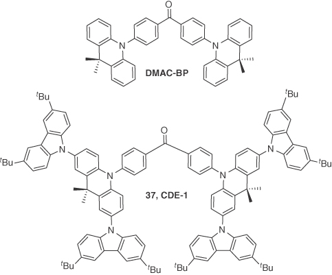
Figure 14.25 Chemical structures of emitter DMAC‐BP and 37.
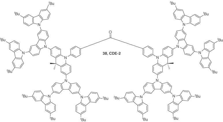
Figure 14.26 Chemical structure of emitter 38.
Ban et al. [48] reported two generations of dendrimers, 39 (TZ‐Cz) and 40 (TZ‐3Cz), based on a triazine core and carbazole donors. They modified the emissive core TZ with different generations of carbazole to produce 39 and 40 and compared their photophysical and EL properties with the emissive core TZ. Both the materials showed an expected blueshift in emission maxima than TZ (502 nm) in neat films (λPL = 490 nm for 39; 487 nm for 40). The thin film ΦPL for 39 and 40 were 58% and 76% under nitrogen‐saturated conditions, both higher than that of TZ (ΦPL = 32%). The thin film ΔEST of TZ, 39, and 40 were 0.28, 0.20, and 0.20 eV, respectively. Solution‐processed, nondoped devices were fabricated using the device structure ITO/PEDOT:PSS (30 nm)/TZ, 39 or 40 (70 nm)/TPBI (40 nm)/Cs2CO3 (2 nm)/Al (100 nm). All the devices showed green emission with λEL of 520 nm. The maximum EQE of the device with 39 was 10.1%, which remained unchanged at a luminance of 1000 cd m−2 and was ten times higher than that of TZ (1.9%). Compound 40 showed an EQE of 6.5% at a luminance of 1000 cd m−2, which was likewise higher than TZ but was inferior to that of 39 indicating the importance of the choice of peripheral dendrons (Figure 14.27).
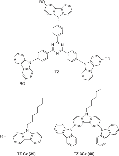
Figure 14.27 Chemical structure of emitter 39 and 40.
14.2 Summary and Outlook
The development of solution‐processed TADF small molecules and macromolecules, including polymers and dendrimers, will continue to draw increasing attention since the initial reports, as summarized in this chapter, demonstrate the viability of these devices, which combine high efficiency with low‐cost fabrication processes. Indeed, the most efficient solution‐processed OLEDs are already approaching their vacuum‐evaporated counterparts. However, their device lifetimes, which is a key performance metric, need considerable further work.
Alongside the development of new soluble materials, an understanding of the structure–property relationships is of equal importance. Thus far, the majority of the solution‐processed TADF emitters have been developed as a function of the incorporation of alkyl or alkoxy groups to an already‐established TADF structure whose efficiencies have already been optimized in the context of a vacuum‐deposited device. At this point, no design rule exists on how to specifically design TADF emitters for solution processing nor are there design rules for which solubilizing groups and how many should be incorporated to control the aggregation‐caused quenching to produce the best films.
Thus, a further improvement in the molecular design, device configuration, and fabrication techniques to tackle device stability issues with solution‐processed TADF emitters is still required. Nonetheless, the tremendous improvement in device performance over the past 3 years augurs well for a future in which low‐cost, high‐performance solution‐processed TADF OLEDs dominate the marketplace.
References
- [1] Tang, C.W. and VanSlyke, S.A. (1987). Appl. Phys. Lett. 51: 913.
- [2] Baldo, M.A., O'Brien, D.F., Thompson, M.E., and Forrest, S.R. (1999). Phys. Rev. B 60: 14422.
- [3] (a) Wilson, J.S., Dhoot, A.S., Seeley, A.J.A.B., Khan, M.S., Kohler, A., and Friend, R.H. (2001). Nature 413: 828.(b) Wohlgenannt, M., Jiang, X.M., Vardeny, Z.V., and Janssen, R.A.J. (2002). Phys. Rev. Lett. 88: 197401.(c) Beljonne, D., Ye, A., Shuai, Z., and Brédas, J.L. (2004). Adv. Funct. Mater. 14: 684.
- [4] (a) Baldo, M.A., O'Brien, D.F., You, Y., Shoustikov, A., Sibley, S., Thompson, M.E., and Forrest, S.R. (1998). Nature 395: 151.(b) Adachi, C., Baldo, M.A., Thompson, M.E., and Forrest, S.R. (2001). J. Appl. Phys. 90: 5048.
- [5] (a) Kim, K.H., Moon, C.K., Lee, J.H., Kim, S.Y., and Kim, J.J. (2014). Adv. Mater. 26: 3844. (b) Lee, C.W. and Lee, J.Y. (2013). Adv. Mater. 25: 5450.
- [6] Partee, J., Frankevich, E.L., Uhlhorn, B., Shinar, J., Ding, Y., and Barton, T.J. (1999). Phys. Rev. Lett. 82: 3673.
- [7] (a) Parker, C.A. and Hatchard, C.G. (1961). Trans. Faraday Soc. 57: 1894.(b) Endo, A., Sato, K., Yoshimura, K., Kai, T., Kawada, A., Miyazaki, H., and Adachi, C. (2011). Appl. Phys. Lett. 98: 083302.(c) Yersin, H. and Monkowius, U. (2008). DE 10 2008 033 563 A1, Germany.
- [8] (a) Endo, A., Ogasawara, M., Takahashi, A., Yokoyama, D., Kato, Y., and Adachi, C. (2009). Adv. Mater. 21: 4802.(b) Deaton, J.C., Switalski, S.C., Kondakov, D.Y., Young, R.H., Pawlik, T.D., Giesen, D.J., Harkins, S.B., Miller, A.J.M., Mickenberg, S.F., and Peters, J.C. (2010). J. Am. Chem. Soc. 132: 9499.
- [9] Cho, Y.J. and Lee, J.Y. (2011). Adv. Mater. 23: 4568.
- [10] Wong, M.Y. and Zysman‐Colman, E. (2017). Adv. Mater. 29: 1605444.
- [11] (a) Yang, X., Xu, X., and Zhou, G. (2015). J. Mater. Chem. C 3: 913.(b) Yang, X., Zhou, G., and Wong, W.Y. (2015). Chem. Soc. Rev. 44: 8484.
- [12] Burroughes, J.H., Bradley, D.D.C., Brown, A.R., Marks, R.N., Mackay, K., Friend, R.H., Burns, P.L., and Holmes, A.B. (1990). Nature 347: 539.
- [13] Burn, P.L., Lo, S.C., and Samuel, I.D.W. (2007). Adv. Mater. 19: 1675.
- [14] (a) Sekine, C., Tsubata, Y., Yamada, T., Kitano, M., and Doi, S. (2014). Sci. Technol. Adv. Mater. 15: 034203.(b) Wu, H.B., Zou, J.H., Liu, F., Wang, L., Mikhailovsky, A., Bazan, G.C., Yang, W., and Cao, Y. (2008). Adv. Mater. 20: 696.(c) Gong, S., Yang, C., and Qin, J. (2012). Chem. Soc. Rev. 41: 4797.
- [15] (a) Kim, H., Byun, Y., Das, R.R., Choi, B.‐K., and Ahn, P.‐S. (2007). Appl. Phys. Lett. 91: 093512.(b) Sonoyama, T., Ito, M., Seki, S., Miyashita, S., Xia, S., Brooks, J., Cheon, K.‐O., Kwong, R.C., Inbasekaran, M., and Brown, J.J. (2008). J. Soc. Inf. Disp. 16: 1229.
- [16] Duan, L., Hou, L., Lee, T.‐W., Qiao, J., Zhang, D., Dong, G., Wang, L., and Qiu, Y. (2010). J. Mater. Chem. 20: 6392.
- [17] Xia, S., Cheon, K.‐O., Brooks, J.J., Rothman, M., Ngo, T., Hett, P., Kwong, R.C., Inbasekaran, M., Brown, J.J., Sonoyama, T., Ito, M., Seki, S., and Miyashita, S. (2009). J. Soc. Inf. Disp. 17: 167.
- [18] Zhong, C., Duan, C., Huang, F., Wu, H., and Cao, Y. (2011). Chem. Mater. 23: 326.
- [19] (a) Halim, M., Pillow, J.N.G., Samuel, I.D.W., and Burn, P.L. (1999). Adv. Mater. 11: 371.(b) Halim, M., Pillow, J.N.G., Samuel, I.D.W., and Burn, P.L. (1999). Synth. Met. 102: 922.
- [20] Lo, S.C., Male, N.A.H., Markham, J.P.J., Magennis, S.W., Burn, P.L., Salata, O.V., and Samuel, I.D.W. (2002). Adv. Mater. 14: 975.
- [21] Kim, K.‐H., Huh, S.‐Y., Seo, S.‐M., and Lee, H.H. (2008). Appl. Phys. Lett. 92: 093307.
- [22] (a) Chen, J., Shi, C., Fu, Q., Zhao, F., Hu, Y., Feng, Y., and Ma, D. (2012). J. Mater. Chem. 22: 5164.(b) Cai, M., Xiao, T., Hellerich, E., Chen, Y., Shinar, R., and Shinar, J. (2011). Adv. Mater. 23: 3590.(c) Jou, J.‐H., Wang, W.‐B., Chen, S.‐Z., Shyue, J.‐J., Hsu, M.‐F., Lin, C.‐W., Shen, S.‐M., Wang, C.‐J., Liu, C.‐P., Chen, C.‐T., Wu, M.‐F., and Liu, S.‐W. (2010). J. Mater. Chem. 20: 8411.(d) Lee, C.W. and Lee, J.Y. (2013). Adv. Mater. 25: 596.
- [23] Hou, L., Duan, L., Qiao, J., Zhang, D., Dong, G., Wang, L., and Qiu, Y. (2010). Org. Electron. 11: 1344.
- [24] (a) Zhu, M., Ye, T., He, X., Cao, X., Zhong, C., Ma, D., Qin, J., and Yang, C. (2011). J. Mater. Chem. 21: 9326. (b) Rehmann, N., Hertel, D., Meerholz, K., Becker, H., and Heun, S. (2007). Appl. Phys. Lett. 91: 103507.
- [25] (a) Yook, K.S. and Lee, J.Y. (2011). Org. Electron. 12: 1711.(b) Gong, S., Fu, Q., Wang, Q., Yang, C., Zhong, C., Qin, J., and Ma, D. (2011). Adv. Mater. 23: 4956.
- [26] Albrecht, K., Matsuoka, K., Fujita, K., and Yamamoto, K. (2015). Angew. Chem. Int. Ed. 54: 5677.
- [27] Mei, L., Hu, J., Cao, X., Wang, F., Zheng, C., Tao, Y., Zhang, X., and Huang, W. (2015). Chem. Commun. 51: 13024.
- [28] Cho, Y.J., Chin, B.D., Jeon, S.K., and Lee, J.Y. (2015). Adv. Funct. Mater. 25: 6786.
- [29] Liu, Y., Xie, G., Wu, K., Luo, Z., Zhou, T., Zeng, X., Yu, J., Gong, S., and Yang, C. (2016). J. Mater. Chem. C 4: 4402.
- [30] Sun, K., Xie, X., Liu, Y., Jiang, W., Ban, X., Huang, B., and Sun, Y. (2016). J. Mater. Chem. C 4: 8973.
- [31] Uoyama, H., Goushi, K., Shizu, K., Nomura, H., and Adachi, C. (2012). Nature 492: 234.
- [32] Cho, Y.J., Yook, K.S., and Lee, J.Y. (2014). Adv. Mater. 26: 6642.
- [33] Tang, C., Yang, T., Cao, X., Tao, Y., Wang, F., Zhong, C., Qian, Y., Zhang, X., and Huang, W. (2015). Adv. Opt. Mater. 3: 786.
- [34] Wong, M.Y., Hedley, G.J., Xie, G., Kölln, L.S., Samuel, I.D.W., Pertegás, A., Bolink, H.J., and Zysman‐Colman, E. (2015). Chem. Mater. 27: 6535.
- [35] Wada, Y., Shizu, K., Kubo, S., Suzuki, K., Tanaka, H., Adachi, C., and Kaji, H. (2015). Appl. Phys. Lett. 107: 183303.
- [36] (a) Takahashi, T., Shizu, K., Yasuda, T., Togashi, K., and Adachi, C. (2016). Sci. Technol. Adv. Mater. 15: 034202.(b) Jang, M.E., Yasuda, T., Lee, J., Lee, S.Y., and Adachi, C. (2015). Chem. Lett. 44: 1248.(c) Zhang, Q., Li, B., Huang, S., Nomura, H., Tanaka, H., and Adachi, C. (2014). Nat. Photonics 8: 326.(d) Tsai, W.‐L., Huang, M.‐H., Lee, W.‐K., Hsu, Y.‐J., Pan, K.‐C., Huang, Y.‐H., Ting, H.‐C., Sarma, M., Ho, Y.‐Y., Hu, H.‐C., Chen, C.‐C., Lee, M.‐T., Wong, K.‐T., and Wu, C.‐C. (2015). Chem. Commun. 51: 13662.
- [37] Xie, G., Li, X., Chen, D., Wang, Z., Cai, X., Chen, D., Li, Y., Liu, K., Cao, Y., and Su, S.J. (2016). Adv. Mater. 28: 181.
- [38] Chen, P., Wang, L.P., Tan, W.Y., Peng, Q.M., Zhang, S.T., Zhu, X.H., and Li, F. (2015). ACS Appl. Mater. Interfaces 7: 2972.
- [39] Yu, L., Wu, Z., Xie, G., Zhong, C., Zhu, Z., Cong, H., Ma, D., and Yang, C. (2016). Chem. Commun. 52: 11012.
- [40] Nikolaenko, A.E., Cass, M., Bourcet, F., Mohamad, D., and Roberts, M. (2015). Adv. Mater. 27: 7236.
- [41] Luo, J., Xie, G., Gong, S., Chen, T., and Yang, C. (2016). Chem. Commun. 52: 2292.
- [42] Lee, S.Y., Yasuda, T., Komiyama, H., Lee, J., and Adachi, C. (2016). Adv. Mater. 28: 4019.
- [43] Zhu, Y., Zhang, Y., Yao, B., Wang, Y., Zhang, Z., Zhan, H., Zhang, B., Xie, Z., Wang, Y., and Cheng, Y. (2016). Macromolecules 49: 4373.
- [44] (a) Ren, Z., Nobuyasu, R.S., Dias, F.B., Monkman, A.P., Yan, S., and Bryce, M.R. (2016). Macromolecules 49: 5452.(b) Nobuyasu, R.S., Ren, Z., Griffiths, G.C., Batsanov, A.S., Data, P., Yan, S., Monkman, A.P., Bryce, M.R., and Dias, F.B. (2016). Adv. Opt. Mater. 4: 597.
- [45] Xie, G., Luo, J., Huang, M., Chen, T., Wu, K., Gong, S., and Yang, C. (2017). Adv. Mater. 29: 1604223.
- [46] Wei, Q., Kleine, P., Karpov, Y., Qiu, X., Komber, H., Sahre, K., Kiriy, A., Lygaitis, R., Lenk, S., Reineke, S., and Voit, B. (2017). Adv. Funct. Mater. 27: 1605051.
- [47] Li, Y., Xie, G., Gong, S., Wu, K., and Yang, C. (2016). Chem. Sci. 7: 5441.
- [48] Ban, X., Jiang, W., Lu, T., Jing, X., Tang, Q., Huang, S., Sun, K., Huang, B., Lin, B., and Sun, Y. (2016). J. Mater. Chem. C 4: 8810.
- [49] Kim, Y.H., Wolf, C., Cho, H., Jeong, S.H., and Lee, T.W. (2016). Adv. Mater. 28: 734.
- [50] Suzuki, Y., Zhang, Q., and Adachi, C. (2015). J. Mater. Chem. C 3: 1700.
- [51] Komatsu, R., Sasabe, H., Inomata, S., Pu, Y.‐J., and Kido, J. (2015). Synth. Met. 202: 165.
- [52] Cao, X., Hu, J., Tao, Y., Yuan, W., Jin, J., Ma, X., Zhang, X., and Huang, W. (2017). Dyes Pigments 136: 543.
- [53] Wada, Y., Shizu, K., Kubo, S., Fukushima, T., Miwa, T., Tanaka, H., Adachi, C., and Kaji, H. (2016). Appl. Phys. Express 9: 032102.
- [54] Zhang, Q., Li, J., Shizu, K., Huang, S., Hirata, S., Miyazaki, H., and Adachi, C. (2012). J. Am. Chem. Soc. 134: 14706.
- [55] Sasabe, H., Gonmori, E., Chiba, T., Li, Y.‐J., Tanaka, D., Su, S.‐J., Takeda, T., Pu, Y.‐J., Nakayama, K.‐i., and Kido, J. (2008). Chem. Mater. 20: 5951.
- [56] Sasabe, H., Tanaka, D., Yokoyama, D., Chiba, T., Pu, Y.‐J., Nakayama, K.‐I., Yokoyama, M., and Kido, J. (2011). Adv. Funct. Mater. 21: 336.
- [57] Lee, T.W., Chung, Y., Kwon, O., and Park, J.J. (2007). Adv. Funct. Mater. 17: 390.
- [58] Tao, Y., Yuan, K., Chen, T., Xu, P., Li, H., Chen, R., Zheng, C., Zhang, L., and Huang, W. (2014). Adv. Mater. 26: 7931.
- [59] Bixon, M., Jortner, J., Cortes, J., Heitele, H., and Michel‐Beyerle, M.E. (1994). J. Phys. Chem. 98: 7289.
- [60] Zhang, Q., Kuwabara, H., Potscavage, W.J. Jr., Huang, S., Hatae, Y., Shibata, T., and Adachi, C. (2014). J. Am. Chem. Soc. 136: 18070.
- [61] Matsushita, T., Asada, T., and Koseki, S. (2007). J. Phys. Chem. C 111: 6897.
- [62] Hatakeyama, T., Shiren, K., Nakajima, K., Nomura, S., Nakatsuka, S., Kinoshita, K., Ni, J., Ono, Y., and Ikuta, T. (2016). Adv. Mater. 28: 2777.
- [63] Lin, T.‐A., Chatterjee, T., Tsai, W.‐L., Lee, W.‐K., Wu, M.‐J., Jiao, M., Pan, K.‐C., Yi, C.‐L., Chung, C.‐L., Wong, K.‐T., and Wu, C.‐C. (2016). Adv. Mater. 28: 6976.
- [64] Kim, M., Jeon, S.K., Hwang, S.H., Lee, S.S., Yu, E., and Lee, J.Y. (2016). Chem. Commun. 52: 339.
- [65] Kaji, H., Suzuki, H., Fukushima, T., Shizu, K., Suzuki, K., Kubo, S., Komino, T., Oiwa, H., Suzuki, F., Wakamiya, A., Murata, Y., and Adachi, C. (2015). Nat. Commun. 6: 8476.
- [66] Wang, H., Xie, L., Peng, Q., Meng, L., Wang, Y., Yi, Y., and Wang, P. (2014). Adv. Mater. 26: 5198.
- [67] Li, J., Nakagawa, T., MacDonald, J., Zhang, Q., Nomura, H., Miyazaki, H., and Adachi, C. (2013). Adv. Mater. 25: 3319.
- [68] Shibata, M., Sakai, Y., and Yokoyama, D. (2015). J. Mater. Chem. C 3: 11178.
- [69] Lo, S.C., Richards, G.J., Markham, J.P.J., Namdas, E.B., Sharma, S., Burn, P.L., and Samuel, I.D.W. (2005). Adv. Funct. Mater. 15: 1451.
- [70] Lee, J., Shizu, K., Tanaka, H., Nomura, H., Yasuda, T., and Adachi, C. (2013). J. Mater. Chem. C 1: 4599.
- [71] (a) Furuta, P., Brooks, J., Thompson, M.E., and Fréchet, J.M.J. (2003). J. Am. Chem. Soc. 125: 13165.(b) Kwon, T.W., Alam, M.M., and Jenekhe, S.A. (2004). Chem. Mater. 16: 4657.
- [72] Zhang, Q., Tsang, D., Kuwabara, H., Hatae, Y., Li, B., Takahashi, T., Lee, S.Y., Yasuda, T., and Adachi, C. (2015). Adv. Mater. 27: 2096.