
13
Thioxanthone (TX) Derivatives and Their Application in Organic Light‐emitting Diodes
Xiaofang Wei, Ying Wang, and Pengfei Wang
Technical Institute of Physics and Chemistry, Chinese Academy of Sciences, Beijing, 100190, China
This chapter summarizes our recent research on the thermally activated delayed fluorescence (TADF) materials based on thioxanthone (TX) derivatives and their application in organic light‐emitting diodes (OLEDs). Synthesis strategies that lead to a series of TX‐based TADF materials are reported, and the tunability of photoluminescent (PL) properties through modifying the molecular structure character of the TX unit is also discussed. Transient and steady‐state photophysical measurement combined with theoretical analyses provides significant insight into their excited‐state properties and intersystem crossing (ISC) process. Efforts have also been devoted to the exploitation of the materials as the emissive materials and hosts for preparation of high‐efficiency OLEDs.
13.1 Organic Light‐emitting Diodes
OLEDs refer to the light‐emitting diodes in which the emissive electroluminescent (EL) layer is composed of a film of organic emissive compounds that emits light in response to electric current. The simplest structure of OLEDs has the emissive layer of organic emitters sandwiched between two electrodes, the anode and cathode, and at least one of the electrodes is transparent. André Bernanose et al. first observed EL in organic materials under high alternating voltage in air in the early 1950s [1]. In 1987, Tang and Slyke of Eastman Kodak Company reported a novel diode device with low operating voltage and improved efficiency, in which two separate hole‐transporting and electron‐transporting layers were incorporated and light emission occurs in the middle of the organic layer [2]. These findings opened the new era of OLEDs. In these devices, organic semiconductors are indispensable as they can be used as the carrier‐transporting/injection materials and emissive materials. These semiconductors are small molecular or polymer materials. Their structures and properties can be tuned to obtain ideal emissive materials with excellent electrical properties. They can also be processed by solution methods, such as inject printing [3], spin‐coating [4], and screen printing [5]. Theoretically, production cost is lower when mass production methods lower the cost. OLEDs can be fabricated on flexible substrates [6], such as polyethylene terephthalate, thereby eliminating fragile and heavy glass substrates and leading to lightweight roll‐up displays. Moreover, OLEDs show low power dissipation, high efficiencies, and excellent color qualities without inherent pronounced directionality, which are superior to those of liquid crystal displays (LCDs). These advantages endow OLEDs with great opportunity for full‐color displays and lighting, and OLEDs have already replayed LCDs in many portable applications [7].
OLEDs are composed of separate carrier‐transporting and carrier‐emitting layers sandwiched between the anode and the cathode. When OLEDs are working, electrons are injected from the cathode, and holes are injected from the anode. Holes and electrons meet in the emissive layer and recombine, leading to the formation of excitons. These excitons, which are located on the emissive molecules, radiatively relax to the ground state and emit the observed EL. Holes and electrons are odd electron species that have a spin of +1/2 or −1/2. Thus, the excitons formed by the recombination of holes and electrons can have either a singlet or triplet configuration. According to the spin statistics, charge carriers injected in OLED recombine to form singlet and triplet excitons at a 1 : 3 ratio. The singlet exciton decays rapidly from S1 to S0, thereby yielding fluorescence, whereas the radiative decay of triplet excitons can lead to phosphorescence. For fluorescence emitters, the first‐generation emitters, the theoretical maximum EL quantum yield of fluorescent emitters is limited to 25% because the radiative transition from the triplet excited state to the singlet ground state is prohibited. Thus, all triplet excitons are lost for the generation of light and transferred into heat dissipation. Therefore, the performance of OLEDs based on these fluorescence emitters is low. For phosphorescent emitters, the second‐generation emitters, strong spin–orbit coupling (SOC) facilitates the radiative path for the emission from triplet to ground state. Efficient transfer from the populated singlet state to the emitting triplet state can also be expected due to the strong SOC. Thus, all the excitons can be transferred to the triplet state for light harvesting, reaching the 100% internal quantum yield. The performance of OLEDs based on them is four times higher efficiency than OLEDs based on fluorescent emitters. However, transition metal ions, such as Ir and Pt, are generally introduced to enhance the SOC in phosphorescent emitters. These noble metals are expensive and indispensable. Their reserves are limited, which increase the cost for the emitters. Phosphorescent emitters require the population of the triplet excitons, and high triplet exciton densities will be produced to achieve high brightness at high current density. The high triplet exciton densities will result in exciton quenching processes, leading to the efficiency roll‐off. Moreover, blue phosphorescent materials often suffer from poor stability and low emission quantum yield. These may limit the implementation of OLEDs in bright display and lighting. Yersin et al. first proposed the application of molecular TADF effect for singlet harvesting in OLEDs [8]. In 2009, Adachi's group reported pure organic aromatic compounds with efficient TADF to attain high EL efficiency (Figure 13.1) [9]. These emitters exhibit a sufficiently small energy gap between the singlet and triplet (ΔEST) to enable upconversion of the triplet excitons to singlet excitons and achieve 100% internal quantum efficiency. High external quantum efficiencies up to 25% have been reported for OLEDs employing TADF emitters, and the TADF emitters have now been accepted as the third generation of OLEDs emitter. Also these TADF materials have been applied to the host of OLEDs.

Figure 13.1 Energy diagram of TADF mechanism is the radiative decay rate from singlet state; krS is the radiative decay rate from singlet state (fluorescence); knrS is the irradiative decay rate from singlet state; knrT is the irradiative decay rate from triplet state; krISC is the rate of the reverse intersystem crossing (rISC) from triplet state to singlet state; TADF is referred to the thermally activated delayed fluorescence; ΔEST is the energy gap between singlet state and triplet state (phosphorescence); S1, S0, and T1 are the energy level of singlet state, ground state, and triplet state.
13.2 Pure Organic TADF Materials in OLEDs
Two distinct mechanisms exist for molecular delayed fluorescence (DF): P‐type DF and E‐type DF. In the P‐type DF mechanism, a DF emission can be caused by a triplet–triplet annihilation. Parker and Hatchard observed P‐type DF for the deoxygenated solutions of pyrene in ethanol [10]. Two molecules in the T1 state can collide with each other in a concentrated solution. The collision provides enough energy for one of the molecules to return to the S1 state and results in emission with the same spectral distribution as normal fluorescence. The decay time constant of the P‐type DF process is half the lifetime of the triplet state in a dilute solution, and the DF intensity shows a quadratic dependence with the excitation light intensity [10]. In the E‐type DF mechanism, the DF fluorescence emission with same spectral distribution as the prompt fluorescence occurs via triplet manifold and then exhibits a much longer decay time constant than the normal fluorescence. Once molecules are excited and achieve the singlet state, ISC to the triplet manifold occurs, followed by reverse ISC (rISC) from the triplet to the singlet state when ΔEST is small and fluorescent emission from the singlet. The cycle of ISC and rISC may repeat several times before fluorescence emission is achieved [11]. Owing to ΔEST between triplet and singlet, the rISC process always corresponds to a thermally activated process, viz the rate constant of the rISC process is strongly temperature dependent. Thus, the fluorescence emission is thermally activated and the E‐type DF is called TADF. TADF is still a rare phenomenon since the first observation of TADF with eosin [12], and for the most fluorophores, TADF is usually much weaker than its prompt fluorescence. In 2011, Prof. Adachi opened up the new pathway for highly efficient EL by harvesting triplet excitons for light emission with aromatic TADF molecules [13]. Enormous efforts have been endeavored to the development of aromatic TADF molecules and their application to the high efficient OLEDs. Versatile molecular systems with TADF have been reported, including spiroacridine, triazine, spirobifluorene, phthalonitrile, diphenyl sulfone derivative, and so on [14]. High external quantum efficiency (EQE) up to 25% has been achieved for OLEDs using TADF emitters. TADF molecules have also been employed as the host for phosphorescent OLEDs to reduce the efficiency roll‐off and increase the device stability [15]. Moreover, TADF materials have been used as assistant dopants for OLEDs based on traditional fluorescent emitters [16, 17]. This chapter focuses on the development and study of TX‐based TADF materials.
13.3 TX Derivatives for OLED
TX (molecular structure shown in Figure 13.2) is a commonly used triplet sensitizer and an archetype of widely used photoinitiators of polymerization reactions, with a radiative decay rate of 5 × 10⁷ s−1 from the singlet state and a lowest triplet energy of 2.80 eV [18]. The fluorescence quantum yield and the maximum fluorescence wavelength of TX increase with the increasing solvent polarity. This is attributed to the proximity effect, that is, the proximity of the S2 (1nπ*) and S1 (1ππ*) singlet excited states of TX leads to the change in the singlet internal conversion [19]. In the nonpolar solvents, S2 and S1 are very close together, and the rate of internal conversion from S1 to S0 is high, leading to a small fluorescence quantum yield and lifetime. In polar hydroxylic solvents, the (1ππ*) states are stablilized, while the (1nπ*) states are destabilized by solute–solvent interactions [20]. Thus, the energy gap between S2 and S1 increases, and the rate of internal conversion from S1 to S0 decreases, leading to a higher fluorescence quantum yield and a longer fluorescence lifetime [20, 21]. The energy gap between the first singlet and triplet excited state of TX had been reported to be lower than 0.3 eV, which is comparable with that of the molecule with efficient TADF [22]. The small ΔEST will enhance the rISC from T1 to S1. ΔEST can also be further reduced by the careful design of organic molecular structures. Thus, TX unit can be regarded as the excellent building blocks for the efficient TADF materials.
Figure 13.2 Molecular structures of TX, TXO‐TPA, and TXO‐PhCz.
13.3.1 High Efficient OLEDs Based on TX‐based TADF Materials
13.3.1.1 Design and Characterization of TX‐based TADF Emitters
For the efficient TADF emitters, the emitters need to show both a small ΔEST and a reasonable radiative decay rate (>106 s−1) to overcome competitive nonradiative decay pathways and get highly luminescent efficiency. TX unit exhibits a radiative decay rate of 5 × 10⁷ s−1. Thus, highly efficient TADF emitters can be obtained by optimizing the molecular structure of TX derivatives to reduce ΔEST and maintain the high radiative decay rate. ΔEST is given by the following equation [13]:
where ES and ET are the energy levels of singlet and triplet excited state; and JLU is the exchange integral between the spatial wave functions of the ground level (the highest occupied molecular orbital (HOMO)) and an excited level (the lowest unoccupied molecular orbital (LUMO)). The exchange integral can be expressed as

where ψH and ψL are the electron wave function of HOMO and LUMO, r1 and r2 are the coordinate of electrons, and r12 is the distance between electrons [23]. Thus, a small ΔEST can be achieved by reducing the overlap of HOMO and LUMO of the molecules. Intramolecular charge‐transfer (ICT) molecules with a donor–acceptor (D–A) structure attain large spatial separation of the wave functions of HOMO and LUMO. Thus, ICT molecules with a D–A structure are constructed based on TX unit and the molecular structures as shown in Figure 13.2. The conventional hole‐transporting moieties of the triphenylamine (TPA) unit or N‐phenylcarbazole (N‐PhCz) unit are introduced as the electron donor unit, and the S atom in TX unit is oxidated to enhance the electron‐accepting ability. The twisted D–A structure facilitates the effective separation of electron densities of the HOMO and LUMO in a single molecule. TXO‐TPA and TXO‐PhCz were synthesized by Suzuki coupling reaction of the 9‐H‐thioxanthen‐9‐one‐10,10‐dioxide (TXO) and the electron donor unit of TPA or PhCz.
In order to qualitatively understand the nature of the excited state of TXO‐TPA and TXO‐PhCz, density functional theory (DFT) calculation was performed at the B3LYP/6‐31G** level with the Gaussian 09 package to investigate their spatial electronic distribution, and the results of the HOMO–LUMO calculation are shown in Figure 13.3. The HOMOs of TXO‐TPA and TXO‐PhCz distribute over the TPA and PhCz moiety, whereas their LUMOs are dispersed on TXO moiety. Only a small overlap was observed between their HOMO and LUMO on the phenyl ring of the TXO moiety with the substituted donor group. These findings indicate the strong charge‐transfer (CT) characteristic of TXO‐TPA and TXO‐PhCz, and a small electron exchange energy and the resulting small ΔEST can also be expected. Time‐dependent DFT calculations were further performed to optimize the geometries for the lowest singlet (S1) and triplet (T1). The effective HOMO–LUMO separation of TXO‐TPA and TXO‐PhCz induced a strong ICT transition. Both compounds exhibited very small ΔEST, 0.03 eV for TXO‐TPA and 0.14 eV for TXO–PhCz, which are much smaller than that of TX and comparable with those reported TADF emitters [24–26].

Figure 13.3 Calculated spatial distributions of the highest occupied molecular orbital (HOMO) and lowest unoccupied molecular orbital (LUMO) electron densities: (a) LUMO and (b) HOMO of TXO‐TPA and (c) LUMO and (d) HOMO of TXO‐PhCz.
Table 13.1 summarizes the absorption and PL peaks of TXO‐TPA and TXO‐PhCz in different solvents and their corresponding quantum yields. TXO‐TPA in all solutions exhibited a CT absorption band associated with the electron transfer from the TPA moiety to TXO moiety at around 415 nm (as shown in Figure 13.4). Similar CT absorption band centered at 400 nm can also be observed for TXO‐PhCz in solutions. All the solutions of TXO‐TPA and TXO‐PhCz emit weak light, when excited by 365 nm, and even no emission can be detected in solvents with high polarity. For TXO‐PhCz and TXO‐TPA, the electronic excitation is also associated with an ICT coupled with rotational relaxation toward a twisted conformation, twisted intramolecular charge transfer (TICT). The nonemittive TICT state provides that additional nonradiative pathway for them, leading to the low quantum efficiency of them in polar solvents. Similar to other TICT compounds [22, 27], a pronounced positive solvatochromism of emission can also be observed: The emission peak shifted to the long wavelength in the solvent with high polarity, and the quantum yield of the solutions decreased with the solvent polarity. We also investigated the phosphorescent emission of TXO‐TPA and TXO‐PhCz at 77 K in oxygen‐free 2‐MeTHF (Figure 13.5). Both compounds exhibit unstructured phosphorescent emission spectra with peaks of 546 and 503 nm for TXO‐TPA and TXO‐PhCz, respectively. The triplet energy levels can be calculated to 2.46 and 2.27 eV for TXO‐TPA and TXO‐PhCz, respectively, from the emission peaks. To avoid the temperature and solvent effect on the PL emission, the PL emission of TXO‐TPA and TXO‐PhCz in 2‐MeTHF at 77 K was also studied to get their ΔEST. TXO‐TPA and TXO‐PhCz in 2‐MeTHF at 77 K showed a PL emission peaks at 555 and 524 nm, respectively. Thus, ΔEST can be estimated to 0.04 eV for TXO‐TPA and 0.09 eV for TXO‐PhCz from the emission peaks of the PL and phosphorescence at 77 K. The large shift of the fluorescence spectra with the temperature can be ascribed to the orientation of the solvent molecules in the reaction field of the electronically excited solute molecules in different temperatures [19]. The ΔEST are comparable with those of TADF emitters of spiroacridine [28], azine derivatives [29–31], spirobifluorene [25], phthalonitrile [9], diphenyl sulfone derivative [32, 33], and anthraquinone [34], and much lower than that of TX derivatives. The small ΔEST possibly endows them TADF properties.
Table 13.1 Absorption and emission characteristics of TXO‐PhCz and TXO‐TPA.
| TXO‐TPA | TXO‐PhCz | |||||
| Solvent | λaba (nm) | λemb (nm) | Φf (10−3) | λab a (nm) | λem b (nm) | Φf (10−3) |
| Hexane | 414 | 555 | 32.3c | 385 | 491 | 26.8 c |
| Toluene | 415 | 586 | 23.6 c | 396 | 522 | 25.4 c |
| 1,4‐Dioxane | 406 | 613 | 15.1 c | 390 | 540 | 22.6 c |
| Chloroform | 424 | 665 | 3.6 c | 400 | 587 | 18.0 c |
| Ethyl acetate | 405 | 663 | 2.1 c | 390 | 573 | 14.9 c |
| THF | 414 | 660 | 2.0 c | 393 | 579 | 5.1 c |
| Ethanol | 420 | n.d. | — | 395 | n.d. | — |
| Acetonitrile | 406 | n.d. | — | 402 | n.d. | — |
| Methanol | 410 | n.d. | — | 413 | n.d. | — |
| Thin film | 450 | 630 | 360d | 420 | 580 | 930 d |
aAbsorption maximum in the long wavelength.
bEmission maximum.
cQuantum yield (±10%) was estimated using quinine sulfate (Φf 54.9% in 1 N H2SO4) as the standard and obtained after nitrogen degassing.
dAbsolute quantum yield, determined with an integrating sphere.
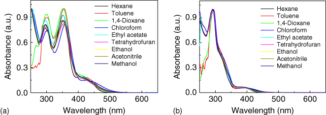
Figure 13.4 Absorption spectra of (a) TXO‐TPA and (b) TXO‐PhCz in different solvents.

Figure 13.5 Phosphorescent and photoluminescence (PL) spectra of (a) TXO‐TPA and (b) TXO‐PhCz in oxygen‐free 2‐Me THF.
The materials and formed films should be stable during the OLEDs fabrication and working. Therefore, we carefully investigated the thermal stability of TXO‐TPA and TXO‐PhCz through the thermal gravimetric analysis (TGA) and differential scanning calorimetry (DSC) under a nitrogen atmosphere. TXO‐TPA and TXO‐PhCz showed good thermal stability: The decomposition temperatures are 380.9 and 392.6 °C for TXO‐TPA and TXO‐PhCz, and the glass transition temperatures are 87.4 and 115.14 °C for TXO‐TPA and TXO‐PhCz. Such excellent thermal stability of them is very convenient for making OLEDs devices and readily endows them with high morphological stability, which is desirable for high‐performance OLEDs during operation.
Figure 13.6 shows the UV–Vis absorption and PL spectra of TXO‐TPA and TXO‐PhCz in thin films. TXO‐PhCz exhibited a broad emission at 570 nm, and TXO‐TPA exhibited an emission peak at 625 nm. The absolute fluorescence quantum yields (ΦPL) of TXO‐PhCz and TXO‐TPA films were 0.93 and 0.36, respectively, which are much higher than those in solutions. Such remarkable PL enhancement in solid states can also be observed in aggregation‐induced emission (AIE) materials. The AIE activity of TXO‐TPA and TXO‐PhCz can be further demonstrated by the emission behavior in acetonitrile/water mixtures with the quantitative change of the water content. Interestingly, the small change in the molecular structure of TXO‐TPA and TXO‐PhCz also leads to the sharp difference in their ΦPL. Thus, the single crystals of TXO‐TPA and TXO‐PhCz were grown, and their structures (as shown in Figure 13.7) were explored by X‐ray single‐crystal analysis. Both molecules showed an asymmetric molecular geometry. The TXO unit was almost in one plane, except the two oxygen atoms connected to the sulfur atom, and the TPA and PhCz units adopted a highly twisted conformation. When in solution, the twisted donor units will undergo intramolecular rotations, leading to the quenching of their emission and the low ΦPL in solution. While in the aggregated state, there are intermolecular short contacts and local interactions between the neighboring molecules. These interactions impeded such intramolecular rotation and rigidified the molecular conformation, leading to the reduction of the loss via nonradiative relaxation. These afforded the high emission of TXO‐TPA and TXO‐PhCz in the solid states [35]. Although only one single bond is changed from TXO‐TPA to TXO‐PhCz, the packing arrangements in their single crystals are totally different. TXO‐TPA molecules in the solid state are held together by the intermolecular π–π interaction and short C–H⋯π contact, and two TXO‐TPA molecules formed a flatly spread dimer with anticonformation with nearly parallel TXO units. Along the a‐axis, TXO‐TPA molecules formed a columnar stacking with an interplanar separation of 3.49 Å, and this columnar stacking affords a large intermolecular π overlap. For TXO‐PhCz, two adjacent molecules with parallel configurations were held together by weaker intermolecular π–π interaction and C–H⋯π short contact and formed a TXO‐PhCz dimer. The C–H⋯π short contact held the dimers in a face‐to‐edge manner, and the dimers were packed tightly in the crystal with the sandwiched herringbone structure. The stronger intermolecular π–π interaction of TXO‐TPA facilitated the transport and thus annihilation of the excitons, leading to the lower ΦPL in solid film.

Figure 13.6 UV–Vis absorption and photoluminescence (PL) spectra of TXO‐TPA and TXO‐PhCz in film.
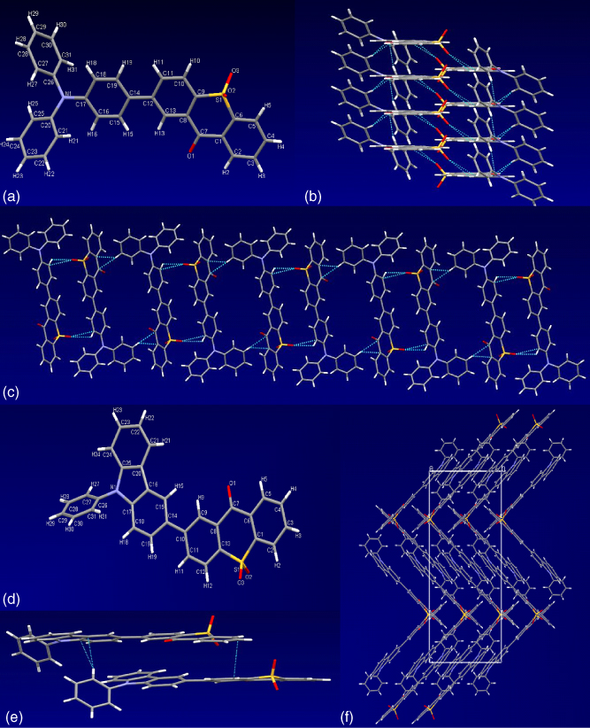
Figure 13.7 Single‐crystal structures of TXO‐TPA and TXO‐PhCz.
To demonstrate the TADF properties of TXO‐TPA and TXO‐PhCz, the transient PL decay of the doped films in the 1,3‐bis(9H‐carbazol‐9‐yl) benzene (mCP) host and their temperature dependence were investigated. The doped films were selected here because TADF mechanism takes place via the triplet manifold. mCP was used as the host due to its high T1 and S1 states, which facilitate the confinement of the triplet excitons within the guest molecules. The emission of the 5 wt% doped TXO‐TPA:mCP film blueshifted to 580 nm with a PL efficiency of 85%. The increased PL efficiency can be ascribed to the suppression of exciton annihilation by doping. The doped film showed a clear second‐order exponential decay at room temperature, and the delay component decayed completely within 78 μs. The delayed component can be significantly suppressed by the oxygen blowing. The presence of the delayed component and the oxygen sensitivity demonstrated that the triplet exciton formed after excitation. The rISC from the triplet to the singlet can be further demonstrated by the overlap of the PL spectra of the prompt and delayed components (inset in Figure 13.8a and b). Figure 13.8 shows the temperature dependence of the transient PL decay from 100 to 300 K. Remarkable temperature dependence can be observed for the delayed component: The delayed component increased from 42% to 82% when the temperature increased from 150 to 300 K. Similar photophysical characteristics were observed for the 5 wt% doped film based on TXO‐PhCz. All these affirm that both TXO‐TPA and TXO‐PhCz exhibit excellent TADF properties. Given that the prompt component showed a very low ratio and no pronounced temperature dependence was observed, the triplet formation efficiency (ΦT) and ΔEST can be derived using the Berberan‐Santos relation from the temperature dependence results [36]:
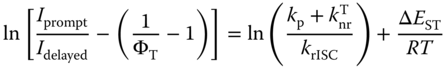
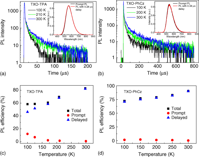
Figure 13.8 Transient photoluminescence (PL) characteristics of TXO‐TPA and TXO‐PhCz films. (a) Temperature dependence of the transient photoluminescence (PL) spectra for 5 ± 1 wt% TXO‐TPA doped in 1,3‐bis(9H‐carbazol‐9‐yl) benzene (mCP) (inset is the PL emission for prompt and for 0.28 μs delay). (b) Temperature dependence of the transient PL spectra for 5 ± 1 wt% TXO‐PhCz doped in mCP (inset is the PL emission for prompt and for 0.38 μs delay). (c) Temperature dependence of the total photoluminescence (black squares), prompt fluorescence (red circles), and delayed fluorescence (blue triangles) for 5 ± 1 wt% TXO‐TPA doped in mCP. (d) Temperature dependence of the total photoluminescence (black squares), prompt fluorescence (red circles), and delayed fluorescence (blue triangles) for 5 ± 1wt%TXO‐PhCz doped in mCP. The determination of the total, prompt, and delayed fluorescence can be referred to [13].
Source: Ref. [13]. Reproduced with the permission of AIP Publishing LLC.
where Iprompt and Idelayed are the intensity of the prompt and delayed components, respectively. kp is the phosphorescence rate constant, ![]() is the nonradiative rate constant from T1, krISC is the T1→S1 rISC rate constant, and R is the gas constant. The ΦT of TXO‐TPA and TXO‐PhCz were 99 and 98%, respectively, indicating that most of the singlet excitons by optical excitation were converted into the triplet excitons. These are consistent with the results that kISC of both compounds are two magnitudes higher than their kr (see Table 13.2). ΔEST of 52 meV for TXO‐TPA and 73 meV for TXO‐PhCz were obtained from the slop of the fitting, which are comparable with the results calculating from the emission spectra and TDDFT.
is the nonradiative rate constant from T1, krISC is the T1→S1 rISC rate constant, and R is the gas constant. The ΦT of TXO‐TPA and TXO‐PhCz were 99 and 98%, respectively, indicating that most of the singlet excitons by optical excitation were converted into the triplet excitons. These are consistent with the results that kISC of both compounds are two magnitudes higher than their kr (see Table 13.2). ΔEST of 52 meV for TXO‐TPA and 73 meV for TXO‐PhCz were obtained from the slop of the fitting, which are comparable with the results calculating from the emission spectra and TDDFT.
Table 13.2 Data extracted from the transient characterization of 5 ± 1 wt% TXO‐TPA:mCP film and 5 ± 1 wt% TXO‐ PhCz:mCP film.
| Compounds | Φtotal (%) | Φprompt (%) | ΦTADF (%) |
ΔEST (meV) |
kS (s−1) |
kISC (s−1) |
ΦT |
knr (s−1) |
kr (s−1) |
| TXO‐TPA | 83.00 | 1.19 | 81.81 | 52 | 3.87 × 10⁷ | 3.79 × 10⁷ | 98 | 5.60 × 10⁴ | 7.44 × 10⁵ |
| TXO‐PhCz | 90.20 | 0.46 | 89.74 | 73 | 5.18 × 10⁷ | 5.13 × 10⁷ | 99 | 4.90 × 10⁴ | 4.51 × 10⁵ |
ks is the rate constant of prompt fluorescence components; kISC is the intersystem crossing rate from singlet to triplet; ΦT is the triplet formation efficiency; and kr and knr are the radiative and nonradiative rate constants from S1 state to S0 state.
The excellent TADF property of the doped films and their thermal stability enabled them to be the emissive molecules for the high‐efficiency OLEDs. The OLED structure was ITO/PEDOT (30 nm)/TAPC (20 nm)/EML (35 nm)/TmPyPB (55 nm)/LiF (0.9 nm)/Al (100 nm), where poly(3,4‐ethylenedioxythiophene) (PEDOT) was used as the hole‐injection layer (HIL) and 1,1‐bis[4‐[N,N′‐di(p‐tolyl)amino]phenyl] cyclohexane (TAPC) was used as the hole‐transporting layer (HTL), 1,3,5‐tri(m‐pyrid‐3‐yl‐phenyl)benzene (TmPyPB) was used as electron‐transporting layer (ETL) and hole‐blocking layer (HBL), and 5 ± 1 wt% TXO‐TPA:mCP or 5 ± 1 wt% TXO‐PhCz:mCP is used as the emitting layer (EML). The molecular structures of the materials in the devices, their energy levels, and the EL characteristics of the devices are shown in Figure 13.9. Both devices showed excellent performances. The devices based on TXO‐TPA emitted yellow light with color coordinates of CIE (0.45, 0.53) and can be turned on at 5.3 V with a maximum current efficiency of 43.3 cd A−1, a maximum power efficiency of 47.4 lm W−1, and a maximum EQE of 18.5%. The devices incorporating TXO‐PhCz emitted green light with a color coordinates of CIE (0.31, 0.56). The devices were turned on at 4.7 V and afforded a maximum current efficiency of 76 cd A−1, a maximum power efficiency of 70 lm W−1, and a maximum EQE of 21.5%. The EQEs of those devices were beyond the theoretical limit of fluorescent OLEDs.
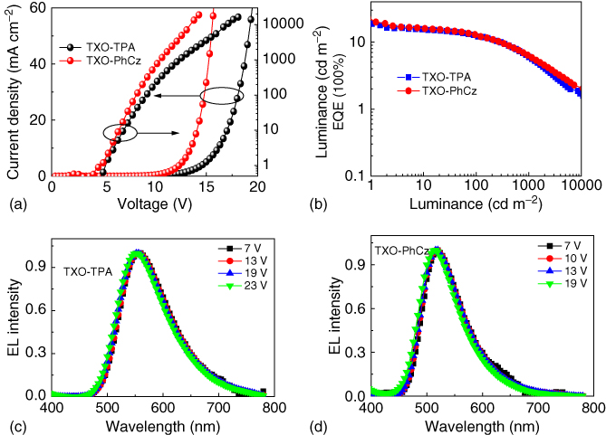
Figure 13.9 Electroluminescent (EL) characteristics of the OLEDs based on TXO‐TPA and TXO‐PhCz. (a) External quantum efficiency (EQE)‐current density characteristics; (b) current density–voltage–luminance characteristics; (c) EL spectra operated at different voltages of the device incorporating TXO‐TPA; and (d) EL spectra operated at different voltages of the device incorporating TXO‐PhCz.
TADF emitters are generally doped into the host to avoid the concentration quenching. Since the host molecules will interact with the TADF emitter molecules, the photophysical properties of the emitters are sensitive to the surroundings. Careful consideration of the intermolecular interactions is promising to construct high‐efficiency OLEDs based on TADF emitters. TXO‐PhCz is the CT molecule with both donor and acceptor units. High‐efficiency OLEDs have been constructed with the hole‐dominating material of mCP as the host. Adachi's group [37] reported a carbazole‐based TADF emitter, 2‐biphenyl‐4,6‐bis(12‐peylindolo[2,3‐a]‐cabazole‐11‐yl)‐1,3,5‐triazine (PIC‐TRZ), with a ΔEST of almost 0 meV. The electron‐dominating material of 9,9′‐(2,6‐pyridinediyl)‐bis‐9H‐carbazole (PYD2) was used as the host of PIC‐TRZ and afforded a high EQE of 14%, higher than that of the compartment with mCP as host. To further enhance the performance of OLEDs based on TXO‐PhCz, the electron‐dominating material of 1,3,5‐Tris(N‐phenylbenzimidazole‐2‐yl)benzene (TPBI) was introduced as the host of TXO‐PhCz [37].
Figure 13.10 showed the absorption of the TXO‐PhCz and TPBI films and PL spectra of TXO‐PhCz:TPBI and pure TPBI films. Large spectra overlap can be observed between the emission of TPBI film and the absorption of TXO‐PhCz film, indicating the efficient energy transfer from TPBI to TXO‐PhCz. The PL spectrum of TXO‐PhCz:TPBI 5 wt% film exhibited only a broad, unstructured emission of TXO‐PhCz countered at 522 nm. No PL emission of TPBI or exciplex of TPBI‐TXO‐PhCz was observed. The PLQY of TXO:TPBI film was 88%, slightly lower than that of TXO‐PhCz in mCP. The transient PL decay of TXO‐PhCz in TPBI host also showed clear second‐order exponential decays (as shown in Figure 13.11). The prompt component was estimated to be 23 ns, corresponding the radiative decay rate constant of 3.8 × 10⁷ s−1 in TPBI. The delayed component was estimated to be 48 μs, shorter than that in mCP (87 μs). The lifetime of the delayed component (τD) can be expressed as [24]

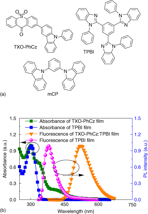
Figure 13.10 (a) Molecular structure of TXO‐PhCz, 1,3,5‐tris(N‐phenylbenzimidazole‐2‐yl)benzene (TPBI), and 1,3‐bis(9H‐carbazol‐9‐yl) benzene (mCP) and (b) absorption of TXO‐PhCz and TPBI films and fluorescence of TXO‐PhCz:TPBI‐doped film and pure TPBI film.

Figure 13.11 Transient photoluminescence (PL) decay of TXO‐PhCz:TPBI‐doped film at 300 K in the time range of (a) 200 ns and (b) 200 μs.
As the PLQYs of TXO‐PhCz in TPBI and mCP are similar, the shorter τD cannot be ascribed to the higher nonradiative decay of triplet excitons. Thus, the temperature dependence of the transient PL decays of the TXO‐PhCz:TPBI film was further investigated. Figure 13.12 shows the dependence of the total PL (ΦTotal), prompt fluorescence (ΦP), and DF (ΦD) of the film on the temperature. As can be observed, ΦP varied very slightly around 13–17% as the temperature between 100 and 250 K, and then, ΦP decreases with the increase of the temperature and reached about 5% at 300 K. ΦD increases monotonically as the temperature increased and saturated to around 82% above 250 K. The synergistic result was that ΦTotal increases monotonically from 100 to 250 K and then decreases above 250 K, leading to the maximum peak of 99% at 250 K. The decrease of the prompt component above was ascribed to the enhanced nonradiative decay from S1 at high temperature. The triplet formation efficiency was estimated to be 99%, and ΔEST is 8.8 meV using the Berberan‐Santos plot. ΔEST was much lower than that of TXO‐PhCz in mCP, which was ascribed to the shift of the singlet and triplet energy levels due to the interaction between host molecule and guest molecule.
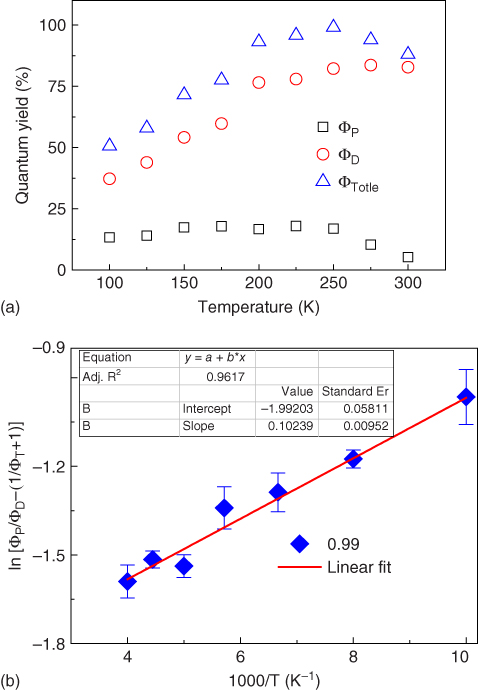
Figure 13.12 (a) Temperature dependence of photoluminescence quantum efficiencies for totle (ΦTotle), prompt (ΦP), and delayed (ΦD) component; and (b) log plot of the intensity ratio of prompt fluorescence to delayed fluorescence versus 1/T.
Multilayer OLEDs were fabricated with TPBI as the host, and the device structure is the following: indium tin oxide (ITO) (150 nm)/poly(3,4‐ethylenedioxythiophene) (PEDOT) (20 nm)/1,1‐bis[4‐[N,N′‐di(p‐tolyl) amino]phenyl] cyclohexane (TAPC) (20 nm)/mCP (10 nm)/TXO‐PhCz:TPBI (5 wt%) (30 nm)/1,3,5‐tri(m‐pyrid‐3‐yl‐phenyl)benzene (TmPyPB) (65 nm)/LiF (0.9 nm)/Al (100 nm). The energy level of the materials in the device and the performance of the device are shown in Figure 13.13. The device was turned on at 5 V with a green emission peak centered at 520 nm. The EL spectra of the device were almost identical to the PL spectra of the TXO‐PhCz:TPBI‐doped film, demonstrating the main contribution of the radiative decay of the singlet of TXO‐PhCz. The device afforded a maximum current efficiency of 71.9 cd A−1, a maximum power efficiency of 45.2 lm W−1, and a maximum EQE of 23.2%, which is higher than those of the device with mCP as the host. These results demonstrated that the higher performance of the device based on TADF emitters can be achieved by the dedicate consideration of the interaction between TADF emitter and host. The novel hosts matching the TADF emitters also are another main path to facilitate the future application of TADF emitter.
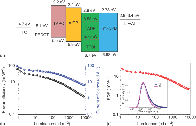
Figure 13.13 (a) The energy levels of the materials involved in the OLEDs based on the emissive layer (EML) of TXO‐PhCz:TPBI‐doped film; (b) current efficiency–luminance–power efficiency characteristics; and (c) external quantum efficiency (EQE)–luminance characteristics. Inset: the electroluminescent (EL) spectrum of the device and photoluminescence (PL) spectrum of TXO‐PhCz:TPBI‐doped film.
It is also significant to construct high‐efficiency OLEDs based on TADF emitters by solution methods [38, 39]. 4,4′,4″‐Tri(9‐carbazoyl)triphenylamine (TCTA) can be easily deposited by the solution method to form amorphous film, and its high first‐triplet energy level (2.78 eV) and wide bandgap can meet the requirement for the host materials for TXO–TPA [40–42]. Figure 13.14 shows the absorption spectrum of TXO‐TPA and the PL spectra of the TCTA film and the 5 wt% TXO‐TPA:TCTA film. A large overlap between the absorption spectrum of TXO‐TPA and the PL spectrum of TCTA was observed, indicating the efficient energy transfer from TCTA to TXO‐TPA. The PL emission of 5 wt% TXO‐TPA:TCTA film showed only a broad emission centered at 570 nm, and there was no other shoulder or emission from TCTA. These findings further demonstrated the efficient energy transfer from TCTA to TXO‐TPA, and no exciplex formed between TCTA and TXO‐TPA. The device structure fabricated here was ITO/PEDOT (30 nm)/TXO‐TPA:TCTA (5 wt%) (30 nm)/ TPBI (50 nm)/LiF (0.9 nm)/Al (100 nm). The emission layer of 5 wt% TXO‐TPA:TCTA was spin‐coated on top of PEDOT layer, and TPBI, LiF, and Al were subsequently deposited by vacuum evaporation to function as the electron‐transport layer, electron‐injection layer, and cathode, respectively. The device can be turned on at 3.5 V with a maximum current efficiency of 15.2 cd A−1, a maximum power efficiency of 13.8 lm W−1, and a maximum EQE of 5.97% (Figure 13.15). The performance of the devices can be further improved by the optimization of the device structure.
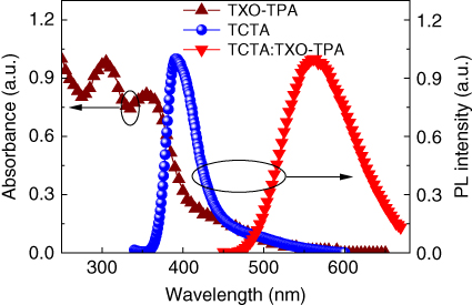
Figure 13.14 Absorbance of TXO‐TPA and photoluminescence (PL) spectra of 4,4′,4″‐tris(carbazole‐9‐yl)triphenylamine (TCTA) film and 5 wt% TXO‐TPA:TCTA‐doped film.
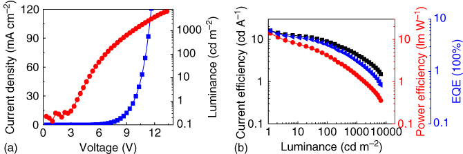
Figure 13.15 Electroluminescence (EL) characteristics: (a) current density–luminance–voltage curve and (b) current efficiency–power efficiency–external quantum efficiency (EQE)–luminance curves.
13.3.1.2 Nondoped OLEDs Based on TADF Emitters with Quantum Well Structure
For the TADF emitters, the triplet excitons can be upconverted into singlet excitons for light harvesting. The triplet excitons can cause the concentration quenching, depressing the efficiency of the devices. Thus, the emitting layer of the host–guest doping systems is the requisite for high‐efficiency OLEDs based on TADF emitters. However, TADF emitters are CT materials, and their photophysical properties are generally sensitive to the molecular atmosphere around the TADF emitters [43, 44]. The doping method with coevaporation is a complicated process and needs the precise control of the concentration of dopant [45]. These will cause the device reproducibility problem, impeding the large‐scale commercial application of TADF OLEDs. Thus, undoped OLEDs based on TADF emitters are highly desirable and promising. Quantum well (QW) structures can effectively confine the charge carriers and excitons inside the emitting layer, affording high‐efficiency light‐emitting diodes [46–48]. These structures have been regarded as an efficient approach to construct nondoped OLEDs to achieve high efficiency. Yang et al. reported the multi‐QW OLEDs based on blue phosphorescent emitter with a peak EQE of 20.31%, current efficiency of 40.31 cd A−1, and power efficiency of 30.14 lm W−1. These excellent results motivated our exploration of undoped TADF OLEDs with QW structure [48].
TXO‐PhCz was chosen as the TADF emitters, and mCP was used as the potential barrier layer for the undoped TADF OLEDs with QW structure. First we optimized the width of the QW. The structures and the performance of the devices with single QW are shown in Figure 13.16, in which a thin layer of TXO‐PhCz was inserted at the center of mCP as the emitting layer. The device with x = 0.5 nm affords a current efficiency of 2.9 cd A−1, a power efficiency of 1.3 lm W−1, and an EQE of 1.2%. Similar performances were obtained for the devices with x = 1 and 1.5 nm, and no prominent thickness dependence of TXO‐PhCz can be observed. The EL spectra of the devices exhibited both blue emission band (370–450 nm) and green emission band. Under the electrical excitation, the radiative decay of mCP and the energy transfer from mCP to TXO‐PhCz for light harvesting will compete each other. The obvious blue band indicated the inefficiency energy transfer from the mCP to TXO‐PhCz. The blue emission bands of the devices were suppressed by the increase of the TXO‐PhCz thickness. Combining with the similar device results, it can be concluded that the energy transfer cannot be enhanced by the increased width of the QW. However, with the increase of the well width, the emission peak redshifted, and the full wave at half maximum (FWHM) of the EL spectra increased. The shift of the emission peak and the change of the FWHM of the emission band for OLEDs coincided with the reported organic single QW devices [49]. Figure 13.17 shows the AFM image of TXO‐PhCz on the multilayer films: ITO/PEDOT (20 nm)/TAPC (20 nm)/TXO‐PhCz (x nm). The mCP film had the very smooth surface with a root‐mean‐square (RMS) of 0.24 nm. With the deposition of TXO‐PhCz, similar smooth surface of TXO‐PhCz film with RMS of 0.243 nm was achieved for the thickness of 0.5 nm. Further increasing the TXO‐PhCz thickness, some bulges formed, and the RMS of TXO‐PhCz films increased. These suggested that TXO‐PhCz film grows on the mCP film via a layer‐by‐layer mode at the beginning stage. Then, the TXO‐PhCz molecules aggregated, leading to the rough surface of the TXO‐PhCz film. The transient PL decay of the TAXO‐PhCz film with different thickness also supported this molecular aggregation (Figure 13.18). All these films exhibited both the prompt and the delayed components for their transient PL decay. For the TXO‐PhCz film with 0.5 nm, the lifetime of the delayed component was about 137 μs. The thicker the TXO‐PhCz film was, the shorter the lifetime of the delayed component of the film was (127 μs for x = 1 nm and 112 μs for x = 1.5 nm). The shorter lifetimes of the delayed component of the films were ascribed to the serious singlet/triplet–triplet annihilation due to the self‐aggregation of TXO‐PhCz molecules. Thus, the width of the QW was better to be 0.5 nm to avoid the singlet/triplet–triplet annihilation.

Figure 13.16 (a) Device structures of OLEDs with single quantum well (QW); (b) the energy‐level diagram of OLEDs with single QW; and the performance of the device with the single QW: (c) current density–voltage–luminance curves; (d) power efficiency–current efficiency–luminance curves; (e) external quantum efficiency (EQE)–luminance curves; and (f) EL spectra.
![Atomic force microscope (AFM) images of the multilayer films of indium tin oxide (ITO)/poly(3,4-ethylenedioxythiophene)-poly (styrenesulfonate) (PEDOT; 20 nm)/di-[4-(N,N′-di-p-tolyl-amino)-phenyl]cyclohexane (TAPC; 20 nm)/1,3-bis(9H-carbazol-9-yl)benzene (mCP; 15 nm)/TXO-PhCz (x nm): (a) 0 m; (b) 0.5 nm; (c) 1 nm; and (d) 1.5 nm.](http://images-20200215.ebookreading.net/4/1/1/9783527339006/9783527339006__highly-efficient-oleds__9783527339006__images__c13f017.jpg)
Figure 13.17 Atomic force microscope (AFM) images of the multilayer films of indium tin oxide (ITO)/poly(3,4‐ethylenedioxythiophene)‐poly(styrenesulfonate) (PEDOT) (20 nm)/di‐[4‐(N,N′‐di‐p‐tolyl‐amino)‐phenyl]cyclohexane (TAPC) (20 nm)/1,3‐bis(9H‐carbazol‐9‐yl) benzene (mCP) (15 nm)/TXO‐PhCz (x nm): (a) 0 nm, (b) 0.5 nm, (c) 1 nm, and (d) 1.5 nm.

Figure 13.18 Transient photoluminescence (PL) decay curves of the multilayer films with the structure of 1,3‐bis(9H‐carbazol‐9‐yl) benzene (mCP) (15 nm)/TXO‐PhCz (x = 0.5, 1, and 1.5 nm)/mCP (15 nm).
To enhance the energy transfer from mCP to TXO‐PhCz, OLEDs with multi‐QWs were constructed. The thickness of the emission layer was fixed to 30 nm, and the 0.5‐nm‐thick TXO‐PhCz layers were symmetrically inserted in mCP layer (as shown in Figure 13.19a). Figure 13.19b and c show the performance of the devices with multi‐QWs. All the devices showed similar turn‐on voltage. With the increase of the QW number, the current densities of the devices at the same voltage first decreased and then increased. The increase of the QW number caused much more defects or traps in TXO‐PhCz films or at mCP/TXO‐PhCz interface, leading to the low current density of the devices. With the increase of the QW number, the thickness of the mCP barrier layer in the EML will decrease, facilitating the direct trapping and thus transporting of the carriers in TXO‐PhCz. These synergistic effects caused the lowest current density of the devices with seven QWs. Similar trend can also be observed for the performance of the devices. The device with seven QWs afforded the highest performance with a current efficiency of 69 cd A−1, a power efficiency of 50 lm W−1, and a maximum EQE of 22.6%. The EL spectra of the devices with QW structure are shown in Figure 13.19d. All the devices exhibited one main emission peak at 520 nm corresponding the emission from TXO‐PhCz. For the two QWs, weak emission at the wavelength lower than 450 nm and an emission shoulder at around 580 nm were also observed, which were ascribed to the inefficient energy transfer from mCP to TXO‐PhCz and the leakage of the excitons into the TAPC layer. The intensity of the emission at 570 nm and wavelengths lower than 450 nm were suppressed as the increase of the number of QWs. This emission disappeared for the device with five or seven QWs. TXO‐PhCz is a bipolar molecular with both donor and acceptor units, and the increased number of QWs shifted the recombination zone to the TAPC/EML interface, leading to the leakage of the excitons to the TAPC layer. All these results demonstrated that the EML with QW structure is a cost‐effective method for the construction of nondoped TADF OLEDs with high efficiency.
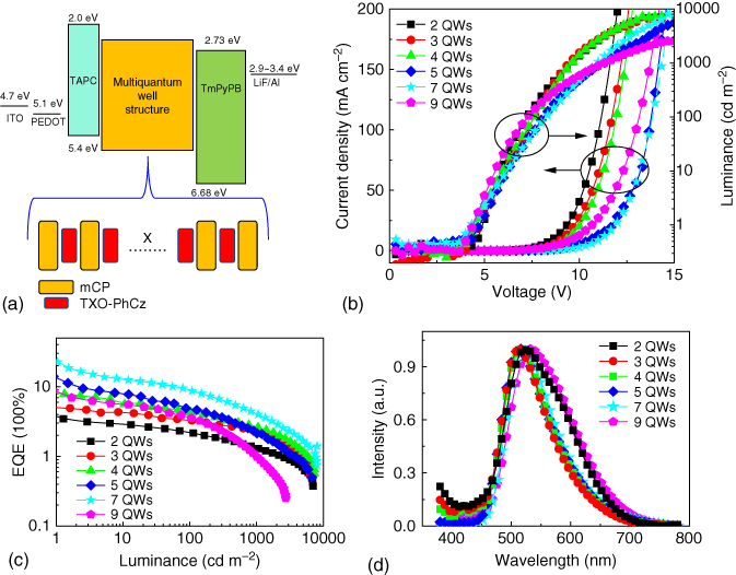
Figure 13.19 Device structures and energy‐level diagram of the multiquantum wells. The thickness of TXO‐PhCz of the quantum wells is fixed to be 0.5 nm (a). X is the number of quantum well, and Y is the thickness of the 1,3‐bis(9H‐carbazol‐9‐yl) benzene (mCP) block layer in the emitting layers: for X = 2, Y = 10 nm; for X = 3, Y = 7.5 nm; for X = 4, Y = 6 nm; for X = 5, Y = 5 nm; for X = 7, Y = 3.75 nm; and for X = 9, Y = 3 nm. Electronic properties of the devices with multiquantum well: (b) current density–voltage–luminance plots, (c) external quantum efficiency (EQE)–luminance plots, and (d) electroluminescence (EL) spectra at 9 V. ITO is referred to indium tin oxide; PEDOT is referred to poly(3,4‐ethylenedioxythiophene)‐poly(styrenesulfonate); TAPC is referred to di‐[4‐(N,N′‐di‐p‐tolyl‐amino)‐phenyl]cyclohexane; LiF is referred to lithium fluoride; Al is referred to aluminum.
13.3.1.3 White OLEDs Based on Blue Fluorescent Emitter and Yellow TX‐based TADF Emitters
Lighting by OLEDs also attracted the commercial interests, and efficient and thin large‐area lighting source is now available in the market [50–52]. Generally, these white organic light‐emitting diodes (WOLEDs) exhibit stable CIE and a color rendition index (CRI) over 75. Highly efficient WOLEDs with a power efficiency of 59.9 lm W−1 and CRI over 80 have been reported using a yellow phosphorescent emitter [53, 54]. As the efficient participation of both singlet and triplet excitons of TADF emitters, it is promising to producing high efficient WOLEDs with nearly 100% internal quantum efficiency [55, 56]. TXO‐TPA emitted yellow EL that was centered at 552 nm with color coordinate of CIE (0.45, 0.53). Thus, it is rational to construct pure fluorescent OLED incorporating blue fluorescent emitter and TXO‐TPA emitter with double‐layer structure.
4P‐NPB is a typical blue fluorescent emitter with a high fluorescent quantum yield of 92% and has been used for highly efficient WOLEDs with phosphorescent emitters [54]. It can be arranged with TXO‐TPA as the two primary‐color emitters for WOLEDs. WOLEDs can be arranged with two emitting layers, and a common host was chosen for the two emitters to reduce structural heterogeneity and facilitate the charge transport in the two emitting layers. mCP was chosen for its high triplet energy level to confine the triplet excitons on the emitters. Its appropriate HOMO and LUMO also facilitated the adjustment of the carrier balance in the emission layer and the construction of highly efficient WOLEDs. The absorbance and PL spectra of 4P‐NPB and TXO‐TPA in thin film and the PL spectra of mCP film are shown in Figure 13.20. mCP showed two sharp emission peaks of 364 and 350 nm with a long tail. 4P‐NPB showed a broad absorption with a peak of 362 nm. Large spectra overlap between the emission of mCP and the absorbance of 4P‐NPB, indicating the efficient energy transfer of the singlet from mCP to 4P‐NPB. Similar overlap can also be observed for the absorbance of TXO‐TPA and the emission of mCP. Therefore, the singlet excitons that formed on the mCP host can be effectively transferred to the two doped emitters through a Förster resonant process. The triplet excitons typically have long diffusion lengths of about 100 nm [57, 58]. The triplet excitons on mCP host can migrate to the TXO‐TPA:mCP layer and transfer to the TXO‐TPA by Dexter transfer process, even if the excitons were generated in the TXO‐TPA:mCP layer. TXO‐TPA can emit yellow light by the efficient upconversion from triplet to singlet. The device structure of WOLED design and the chemical structure and energy level of the used materials are shown in Figure 13.21. mCP shows a high hole mobility of 1.2 × 10⁻⁴ cm2 V−1 s−1, which was three times higher than that of electron mobility [59]. Similarly, the hole mobility of 4P‐NPB is significantly higher than that of the electron mobility [60]. Thus, the exciton generation zone will be located at the interface of 4P‐NPB:mCP and TmPyPB layer. Although some exciton losses in the transfer processes cannot be avoided, unity internal quantum efficiency can be achieved for the high efficient WOLEDs.

Figure 13.20 The absorption spectrum of N,N′‐di‐(1‐naphthalenyl)‐N,N′‐diphenyl‐[1,1′:4′,1″:4‴,1‴‐quaterphenyl]‐4‐4‴‐diamine (4P‐NPB) and TXO‐TPA thin films and photoluminescence (PL) spectra of 1,3‐bis(9H‐carbazol‐9‐yl) benzene (mCP), 4P‐NPB, and 5 wt% TXO‐TPA:di‐[4‐(N,N′‐di‐p‐tolyl‐amino)‐phenyl]cyclohexane (TAPC) film.
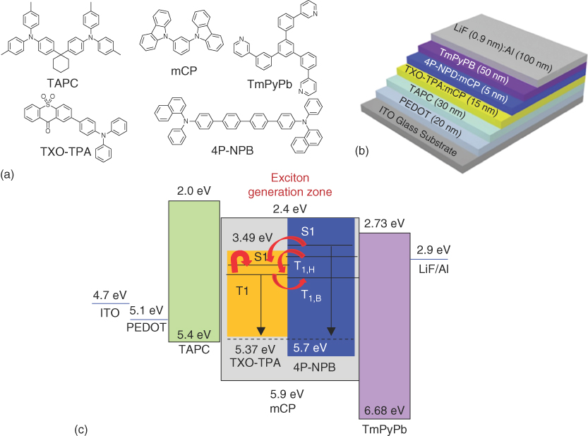
Figure 13.21 (a) The molecular structure of the materials used for the construction of white OLEDs (WOLEDs); (b) device structure and molecule arrangement of the WOLEDs; and (c) energy‐level scheme for materials used in the WOLEDs and exciton energy diagram of the emitting layers.
To get high efficient WOLED, the balance of yellow emission and blue emission can be tuned by the delicate management of singlet and triplet excitons in the two emitting layers. The doped concentration of TXO‐TPA was maintained at 5 wt% as highly efficient yellow OLEDs have been achieved. The doping concentration of 4P‐NPB was optimized from 0.5 to 20 wt%. The performances of the devices are summarized in Table 13.3. The devices showed similar turn‐on voltages of about 4 V. Yellow light can only be emitted for the device with a 4P‐NPB doping concentration of 0.5 wt%. By increasing the doping concentration of 4P‐NPB, the blue emission peak appeared, and its intensity increased. The color coordinate shifts from the yellow light region into the white region (Figure 13.22). When the doping concentration was increased to 20 wt%, only blue light was observed, and no emission from TXO‐TPA was observed. At low doping concentration of 4P‐NPB, the singlet harvested for blue light, thereby leading to the yellow emission alone. The loss of singlet and triplet excitons during diffusion led to low efficiency, whereas the nonradiative loss of triplet excitons on 4P‐NPB trapped by Dexter energy transfer diminished the efficiency of the devices at high doping concentration of 4P‐NPB. Moreover, the back Dexter transfer from TXO‐TPA to 4P‐NPB at the interface of the two emission layers is another possible reason for triplet exciton loss (Figure 13.21c). Thus, the optimized concentration of 4P‐NPB is 5 wt%, and the device affords a current efficiency of 10.9 cd A−1, a power efficiency of 8.5 lm W−1, and an EQE of 4.4%. The maximum total efficiencies of the devices can be up to 18.5 cd A−1, 14.5 lm W−1, and 7.5%, which are comparable with those of the devices based on fluorescent and phosphorescent emitters with similar structures [58]. Notably, the EL spectra of the device were very stable, and no derivation of the peak intensity and new peaks was observed even at high voltage up to 10 V.
Table 13.3 Electroluminescence characteristics of the OLEDs with different doping concentrations of 4P‐NPB.
| Maximum values | |||||
| Doping concentration of 4P‐NPB (%) | Turn‐on voltage (V) | Current efficiency (cd A−1) | Power efficiency (lm W−1) | EQE (%) | Color coordinate at 6 V |
| 0.5 | 4 | 5.6 | 2.9 | 2.0 | (0.39, 0.51) |
| 2 | 4 | 10.9 | 8.5 | 4.4 | (0.37, 0.42) |
| 5 | 4 | 7.2 | 5.7 | 3.6 | (0.31, 0.35) |
| 10 | 4.1 | 4.9 | 2.4 | 2.5 | (0.30, 0.33) |
| 20 | 4 | 3.2 | 1.5 | 1.9 | (0.27, 0.27) |
![Images of color coordinate of International Commission on Illumination (CIE) at 6 V for the devices with different doping concentrations. 4P-NPB is referred to N,N′-di-(1-naphthalenyl)-N,N′-diphenyl-[1,1′:4′,1′′:4′′,1′′′-quaterphenyl]-4-4′′′-diamine.](http://images-20200215.ebookreading.net/4/1/1/9783527339006/9783527339006__highly-efficient-oleds__9783527339006__images__c13f022.jpg)
Figure 13.22 Color coordinate of International Commission on Illumination (CIE) at 6 V for the devices with different doping concentrations. 4P‐NPB is referred to N,N′‐di‐(1‐naphthalenyl)‐N,N′‐diphenyl‐[1,1′:4′,1″:4″,1‴‐quaterphenyl]‐4‐4‴‐diamine.
To optimize the CIE and the performance of WOLEDs, device I, II, and III were fabricated, and the device structures were as follows: device I: ITO/PEDOT (20 nm)/TAPC (40 nm)/TPA:mCP (5%) (5 nm)/4P‐NPB:mCP (2%) (5 nm)/TmPyPB (50 nm)/LiF(0.9 nm)/Al (100 nm); device II: ITO/PEDOT (20 nm)/TAPC (40 nm)/TPA:mCP (5%) (10 nm)/4P‐NPB:mCP (2%) (10 nm)/TmPyPB (50 nm)/LiF (0.9 nm)/Al (100 nm); device III: ITO/PEDOT (20 nm)/TAPC (40 nm)/TPA:mCP (5%) (10 nm)/mCP (5 nm)/4P‐NPB:mCP (2%) (10 nm)/TmPyPB (50 nm)/LiF (0.9 nm)/Al (100 nm). All these devices showed white EL emission. Device II and III with broad yellow‐emitting layers showed higher performance due to the diminished quenching effect of the triplet excitons. As shown in Table 13.4, device II showed the highest performance: The device can be turned on at 4 V with a maximum EQE of 4.7%, a current efficiency of 8.1 cd A−1, and a power efficiency of 6.4 lm W−1. Impressively, the device showed low‐efficiency roll‐off. The critical current density of the device where EQE declines to half of its peak was approximately 112 mA cm−2, which is among the best of reported multilayer WOLED based on phosphorescent emitters. No interlayer is needed to prevent the mutual exciton transfer and quenching [54].
Table 13.4 Electroluminescence characteristics of the devices I, II, and III.
| Maximum values | |||||
| Device structure | Turn‐on voltage (V) | Current efficiency (cd A−1) | Power efficiency (lm W−1) | EQE (%) | Color coordinate at 6 V |
| Device I | 3.6 | 3.2 | 2.4 | 1.8 | (0.35, 0.32) |
| Device II | 4.0 | 8.1 | 6.4 | 4.7 | (0.34, 0.34) |
| Device III | 4.3 | 8 | 5.8 | 4.4 | (0.37, 0.36) |
13.3.2 TADF Host for Phosphorescent Emitters
TADF materials can also be applied as the host of phosphorescent OLEDs, which is inspired by their fast rISC from triplet to singlet. Generally, the efficiency of phosphorescent OLEDs tends to decrease with increasing brightness, the so‐called efficiency “roll‐off.” The serious efficiency roll‐off impedes them from the applications requiring high brightness [61]. There are two main annihilation processes on host molecules that are most relevant to the EQE roll‐off of phosphorescent OLEDs: triplet–triplet and triplet‐polaron annihilations. Thus, the efficiency roll‐off can be effectively alleviated by the reduction of the triplet exciton density on the host materials. Lee's group [62] reported the exciplex with TADF properties as the host for the fluorescent emitter to sensitize the triplet excitons in the fluorescent OLEDs through the fast rISC process of the exciplex, and high‐performance fluorescent OLEDs with EQE of 14.5% were achieved, which surpassed the efficiency limitation of fluorescent OLEDs. The exciplex host was the main carrier recombination center, and the triplet excitons were upconverted into the singlet excitons and then resonantly transferred to the singlet of fluorescent molecules for light emission. Thus, reducing the triplet exciton density by using TADF molecules as the host of phosphorescent emitter [16, 17] and alleviating the efficiency roll‐off of phosphorescent OLEDs are rational.
MTXSFCz (Figure 13.23) was synthesized by Suzuki coupling reaction, in which the hole‐transporting PhCz and electron‐withdrawing TX unit were bridged with unconjugated fluorene. The HOMO of MTXSFCz was mainly localized on the PhCz unit, and the LUMO was dispersed over the electron‐withdrawing TX unit. No obvious overlap between HOMO and LUMO was observed, which is similar to the reported bipolar phosphorescent host [63, 64]. The unconjugated fluorine unit caused the effective separation of the electron densities of HOMO and LUMO, leading to a small ΔEST of 0.06 eV calculated on the ground‐state geometries. The small ΔEST facilitated the upconversion process from triplet to singlet. MTXSFCz showed a high decomposition temperature of 456 °C and a high glass transition temperature of 127.3 °C. The excellent stability and the twisted structure were beneficial to form homogeneous and amorphous films with good stability [65]. MTXSFCz exhibited bipolar charge transport properties with a hole and electron mobilities of 1.45 × 10⁻⁵ and 1.75 × 10⁻⁸ cm2 (V s)−1, respectively.

Figure 13.23 (a) Molecular structure of MTXSFCz and (b) calculated spatial distributions of the highest occupied molecular orbital (HOMO) and lowest unoccupied molecular orbital (LUMO) electron densities of MTXSFCz by Gaussian 03 at the B3LYP/6‐31G(d) level.
There was an absorption peak around 380 nm arising from the n–π* transition of TX core in the UV–Vis absorption spectrum [19, 21, 66], and no prominent CT absorption was observed over 400 nm [21] (see Figure 13.24). The HOMO energy level of −5.57 eV can be obtained from the cyclic voltammetry, and the LUMO energy level can be estimated to −2.83 eV, combining the energy gap estimated from the onset of the absorption spectrum. MTXSFCz in the DCM solution emitted blue light with a peak centered at 420 nm, and the emission peak in neat film centered at 451 nm, redshifted approximately 30 nm. The PL quantum yield of the MTXSFCz neat film measured by the integrating sphere was only 5.1%, and the low PL quantum yield was beneficial for the construction of highly efficient phosphorescent OLEDs. The triplet energy of 2.71 eV was estimated from its phosphorescent spectrum measured in oxygen‐free 2‐methyl THF at 77 K. Thus, ΔEST was estimated to be 0.19 eV, which is comparable with that from the DFT calculation and those of the reported TADF materials [14, 64].
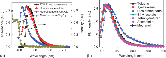
Figure 13.24 (a) Absorbance, photoluminescence (PL) of MTXSFCz in CH2Cl2 and in film, and spectrum measured in oxygen‐free 2‐methyl tetrahydrofuran (2‐MeTHF) at 77 K and (b) PL emission of MTXSFCz in different solvents.
The transient PL decay of the doped film of MTXSFCz in mCP and the temperature dependence were performed to demonstrate the TADF properties of MTXSFCz further (as shown in Figure 13.25). The doped film emitted blue light with the emission peak at 455 nm, and no emission from mCP was observed. The emission spectra of the film blueshifted due to the temperature dependence of the relaxation process, and the relative intensity decreased when the film is cool down to lower temperature [67, 68]. The PL decay curves were resolved into two components: the prompt and delayed components. The transient decay times of the prompt and delayed components were 3.1 ns and 45.3 μs from second‐order exponential decay fitting. The PL spectra of these two components were identical. Thus, the DF can be assigned to the TADF that occurs through rISC. This finding can be further demonstrated by the monotonically increase of the delayed component as the temperature increases [24].

Figure 13.25 (a) Temperature dependence of the photoluminescence (PL) intensity for 5 ± 1 wt% MTXSFCz doped in 1,3‐bis(9H‐carbazol‐9‐yl) benzene (mCP) and inset is the PL decay curve of the doped film at 300 K. (b) Temperature dependence of prompt proportion (red circles) and delayed proportion (blue triangles) for 5 ± 1 wt% MTXSFCz doped in mCP based on lifetime fitting results. (c) The photoluminescence spectrum of the same film without delay time and 6 μs delay time. The determination of the total, prompt, and delayed fluorescence can be referred to [24].
Source: Ref. [24]. Reproduced with the permission of Springer Nature.
Efficient Förster energy transfer from MTXSFCz to Ir(pig)2acac and Ir(2‐phq)3 (molecular structure as shown in Figure 13.26) can be expected due to the overlap between the PL emission of MTXSFCz and the absorption of Ir(pig)2acac and Ir(2‐phq)3. Thus, phosphorescent OLEDs based on MTXSFCz were fabricated, and the device structure was ITO/PEDOT (30 nm)/TAPC (20 nm)/10 wt% Ir(pig)2acac: MTXSFCz or Ir(2‐phq)3: MTXSFCz (35 nm)/TmPyPB (55 nm)/LiF (0.9 nm)/Al (100 nm). The energy‐level diagram was shown in Figure 13.26, and the device results were shown in Table 13.5. All devices were turned on at a voltage of about 4.0 V, and the EL spectra were independent of the applied voltage. The orange device with CIE (0.56, 0.43) showed a maximum current efficiency of 26.8 cd A−1, a maximum power efficiency of 18.0 lm W−1, and a maximum EQE of 11.8%. The red device with CIE (0.68, 0.32) afforded a current efficiency of 13.8 cd A−1, a power efficiency of 8.2 lm W−1, and an EQE of 15.6%. Interestingly, the efficiency roll‐offs of both devices were low. J0, the current density at which the EQE drops to half of its maximum value, was 80 mA cm−2 for the orange devices and 174 mA cm−2 for the red devices. These values are much larger than those of reported phosphorescent OLEDs and that of the reference devices based on mCP [68–73].
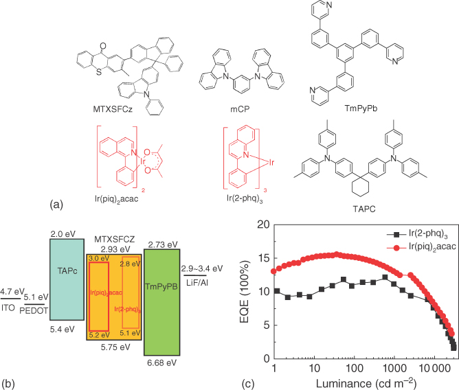
Figure 13.26 (a) The molecular structures of the semiconductors in the construction of the phosphorescent OLEDs; (b) the energy‐level scheme for the phosphorescent OLEDs based on MTXSFCz; and (c) external quantum efficiency (EQE)–luminance curves of the phosphorescent OLEDs based on MTXSFCz. The doping concentration of the phosphorescent guest is 10 wt%. ITO is referred to indium tin oxide; PEDOT is referred to poly(3,4‐ethylenedioxythiophene)‐poly(styrenesulfonate); LiF is referred to lithium fluoride; Al is referred to aluminum.
Table 13.5 The performance summary of orange and red PhOLEDs based on reported hosts and MTXSFCz.
| Device | Voltage (V) | Dopant concentration (wt%) | Current efficiency (cd A−1) | Power efficiency (lm W−1) | EQEMax (%) | EQE (%) at 1 000 cd m−2 | EQE (%) at 10 000 cd m−2 |
| Ir(2‐phq)3 | 4.0 | 10 | 26.8 | 18.0 | 11.8 | 11.2 | 7.6 |
| 4.0 | 5 | 19.6 | 15.4 | 8.6 | 7.9 | 5.8 | |
| Ir(piq)2acac | 4.4 | 10 | 13.8 | 8.2 | 15.6 | 13.1 | 8.0 |
| 3.8 | 5 | 10.5 | 8.6 | 12.0 | 9.4 | — |
To confirm that the TADF properties of the MTXSFCz host can alleviate the efficiency roll‐off, the decay curves of 5 wt% Ir(pig)2acac‐doped films with MTXSFCz and mCP were investigated (as shown in Figure 13.27). For the low doping concentration, the main emission of the doped film harvested from the triplet state of the guest through the FRET from the host to the guest [74, 75]. The decay time of the Ir(piq)2acac emission in vacuum was about 864.4 ns. The decay time and the intensity of the emission were suppressed upon exposure to air. Meanwhile, no such effect was observed for the emission of Ir(piq)2acac in mCP. Thus, the quenching effect of oxygen on Ir(piq)2acac emission in MTXSFCz was attributed to the storage of the triplet excitons on MTXSFCz [76]. Both mCP and MTXSFCz had high triplet energy, at least 0.7 eV higher than that of Ir(piq)2acac. All triplet excitons were confined on Ir(piq)2acac guest, and thus, similar decay dynamics and lifetime should be observed [77]. However, the lifetime of Ir(piq)2acac in MTXSFCz in vacuum was 864.4 ns, about 100 ns longer than that of Ir(piq)2acac in mCP (764.3 ns). The longer lifetime can be attributed to the presence of the ISC and rISC on photoexcited MTXSFCz (as shown in Figure 13.28). The rate constant of FRET from host to guest can be estimated from the following equation [78]:
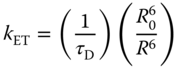
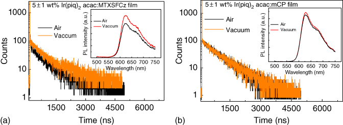
Figure 13.27 (a) The lifetime of 5 ± 1 wt% Ir(piq)2acac:MTXSFCz film in vacuum and in air and inset is the photoluminescence (PL) intensity of 5 ± 1 wt% Ir(piq)2acac:MTXSFCz film in vacuum and in air. (b) The lifetime of 5 ± 1 wt% Ir(piq)2acac:1,3‐bis(9H‐carbazol‐9‐yl) benzene (mCP) film in vacuum and in air and the inset is the PL intensity of 5 ± 1 wt% Ir(piq)2acac:mCP film in vacuum and in air.

Figure 13.28 The mechanism of the energy transfer from the host to Ir(piq)2acac in (a) MTXSFCz and (b) 1,3‐bis(9H‐carbazol‐9‐yl) benzene (mCP). Since the doping concentration of both host–guest system is low, the Dexter energy transfer from MTXSFCz to Ir(piq)2acac can be omitted. The cycling of the exciton between singlet and triplet will contribute to the longer lifetime of Ir(piq)2acac emission in MTXSFCz.
where τD is the radiative decay time of donor molecular, R0 is the Förster transfer radius, and R is the average distance between donor and acceptor molecules. R0 of the Ir(piq)2acac:MTXSFCz film was 2.6 nm using a molecular modeling program, and the rate constant was >1010 s−1, which was nearly two orders of magnitude faster than those of ISC and rISC of TADF molecules [79]. The fast FRET converted the electrically generated singlet excitons of the host to the singlet and triplet excitons of guest, thereby facilitating the rISC of the MTXSFCz host from triplet to singlet. These decreased the triplet concentration on the MTXSFCz host, leading to the low‐efficiency roll‐off of the devices based on the MTXSFCz host.
13.4 Concluding Remarks and Outlook
TADF materials have attracted much attention in recent years due to their wide application in OLEDs, such as emitter, host, sensitizer of fluorescent emitters, and so on. TX unit, which benefited from both ketone and sulfur connections, showed a very small singlet–triplet energy gap, indicating its potential application in the construction of TADF materials. We reported high green and yellow TADF emitters, namely, TXO‐TPA and TXO‐PhCz, by the incorporation of donor units of TPA or PhCz and oxidation of sulfur atoms. The photophysical results of the emitters demonstrated their very small ΔEST (0.052 and 0.073 eV), which afforded fast rISC from triplet to singlet. The high‐efficiency OLEDs based on TXO‐TPA and TXO‐PhCz showed a maximum EQE of 18.5 and 21.5%, respectively. These values surpassed the limitation of the OLEDs based on traditional fluorescent emitters. The high‐efficiency multilayer WOLEDs incorporating 4P‐NPB and TXO‐TPA showed a maximum EQE of 4.7% with a CIE coordinate of (0.34, 0.34). We also reported the phosphorescent host of MTXSFCz with TADF, which had a TX and PhCz unit linked by spirofluorene. The orange and red PHOLEDs based on the host showed the high maximum EQE of 11.8 and 15.6%, respectively. The efficient rISC of the host suppressed the subdued annihilation of the triplet on the host, resulting in the low‐efficiency roll‐off. These works will be helpful in the development of new TADF materials for highly efficient OLEDs.
Our studies are only the primary step in the exploration of the TX‐based TADF materials. Thus, the relationship between the molecular structures of the TX system and their photophysical properties should be studied for the rational design of TADF materials. Blue TADFs based on TX unit are particularly indispensable for the construction of OLEDs for the display and lightings. Solution‐processed TADF emitters are also appealing for the low‐cost OLEDs. Furthermore, new TADF hosts based on TX unit are also an interesting topic. Further studies should focus on the rational design of TADF hosts and their application in blue phosphorescent OLEDs. Moreover, the use of TADF materials is not limited to the emitters or hosts. OLEDs with TADF emitters as the sensitizer of fluorescent emitters had been reported. Thus, the new applications of TADF materials based on TX, such as sensitizer or other applications, are another further step toward the realization of highly efficient OLEDs.
Acknowledgments
This work was financially supported by the National Natural Science Foundation of China (Grant No. 61420106002, No.51373189, No. 61178061, and No.61227008), the “Hundred Talents Program” of the Chinese Academy of Sciences, and the Start‐Up Fund of the Technical Institute of Physics and Chemistry of the Chinese Academy of Sciences.
References
- [1] Bernaose, A., Comte, M., and Vouaux, P. (1953). J. Chim. Phys. 50: 261.
- [2] Tang, C.W. and Vanslyke, S.A. (1987). Appl. Phys. Lett. 51: 913.
- [3] Seki, S., Uchida, M., Sonoyama, T., Ito, M., Watanabe, S., Sakai, S., and Miyashita, S. (2012). SID Symposium Digest of Technical Papers 40: 593.
- [4] Cai, M., Xiao, T., Hellerich, E., Chen, Y., Shinar, R., and Shinar, J. (2011). Adv. Mater. 23: 3590.
- [5] Lee, D.‐H., Choi, J.S., Chae, H., Chung, C.‐H., and Cho, S.M. (2008). Display 29: 436.
- [6] Li, Y., Tan, L.W., Hao, X.T., Ong, K.S., and Zhu, F. (2005). Appl. Phys. Lett. 86: 153508.
- [7] Gaspar, D.J. and Polikarpov, E. (2015). OLED Fundamentals‐Materials, Device, and Processing of Organic Light‐Emitting Diodes. Boca Raton: CRC Press.
- [8] Yersin, H. and Monkowius, U. (2006). DE 10 2008 033 563. Germany: Internal filing at the University of Regensburg.
- [9] Endo, A., Ogasawara, M., Takahashi, A., Yokoyama, D., Kato, Y., and Adachi, C. (2009). Adv. Mater. 21: 4802.
- [10] Parker, C.A. and Hatchard, C.G. (1961). Trans. Faraday Soc. 57: 1894.
- [11] Baleizão, C. and Berberan‐Santos, M.N. (2007). J. Chem. Phys. 126: 204510.
- [12] Valeur, B. (ed.) (2002). Molecular Fluorescence: Principles and Applications. Weinheim: Wiley‐VCH.
- [13] Endo, A., Sato, K., Yoshimura, K., Kai, T., Kawada, A., Miyazaki, H., and Adachi, C. (2011). Appl. Phys. Lett. 98: 083302.
- [14] Tao, Y., Yuan, K., Chen, T., Xu, P., Li, H., Chen, R., Zheng, C., Zhang, L., and Huang, W. (2014). Adv. Mater. 26: 7931.
- [15] Wang, H., Meng, L., Shen, X., Wei, X., Zheng, X., Lv, X., Yi, Y., Wang, Y., and Wang, P. (2015). Adv. Mater. 27: 5861.
- [16] Nakanotani, H., Higuchi, T., Furukawa, T., Masui, K., Morimoto, K., Numata, M., Tanaka, H., Sagara, Y., Yasuda, T., and Adachi, C. (2014). Nat. Commun. 5: 4016.
- [17] Zhang, D., Duan, L., Li, C., Li, H., Zhang, D., and Qiu, Y. (2014). Adv. Mater. 26: 5050.
- [18] Fouassier, J.P. and Ruhlmann, D. (1993). Eur. Polym. J. 29: 505.
- [19] Lai, T. and Lim, E.C. (1980). Chem. Phys. Lett. 73: 244.
- [20] Cavaleri, J.J., Prater, K., and Bowman, R.M. (1996). Chem. Phys. Lett. 259: 495.
- [21] Ley, C., Morlet‐Savary, F., Jacques, P., and Fouassier, J.P. (2000). Chem. Phys. 255: 335.
- [22] Allonas, X., Ley, C., Bibaut, C., Jacques, P., and Fouassier, J.P. (2000). Chem. Phys. Lett. 322: 483.
- [23] Shuai, Z. and Peng, Q. (2016). Nat. Sci. Rev. doi: 10.1093/nsr/nww024.
- [24] Uoyama, H., Goushi, K., Shizu, K., Nomura, H., and Adachi, C. (2012). Nature 492: 234.
- [25] Nakagawa, T., Ku, S.‐Y., Wong, K.‐T., and Adachi, C. (2012). Chem. Commun. 48: 9580.
- [26] Lee, C.W. and Lee, J.Y. (2014). Chem. Mater. 26: 1616.
- [27] Soujanya, T., Fessenden, R.W., and Samanta, A. (1996). J. Phys. Chem. 100: 3507.
- [28] Méhes, G., Nomura, H., Zhang, Q., Nakagawa, T., and Adachi, C. (2012). Angew. Chem. Int. Ed. 51: 11311.
- [29] Li, J., Nakagawa, T., MacDonald, J., Zhang, Q., Nomura, H., Miyazaki, H., and Adachi, C. (2013). Adv. Mater. 25: 3319.
- [30] Serevičius, T., Nakagawa, T., Kuo, M.‐C., Cheng, S.‐H., Wong, K.‐T., Chang, C.‐H., Kwong, R.C., Xia, S., and Adachi, C. (2013). Phys. Chem. Chem. Phys. 15: 15850.
- [31] Hirata, S., Sakai, Y., Masui, K., Tanaka, H., Lee, S.Y., Hiroko, N., Nakamura, N., Yasumatsu, M., Nakanotani, H., Zhang, Q., Shizu, K., Miyazaki, H., and Adachi, C. (2015). Nat. Mater. 14: 330.
- [32] Zhang, Q., Li, B., Huang, S., Nomura, H., Tanaka, H., and Adachi, C. (2014). Nat. Photon. 8: 326.
- [33] Zhang, Q., Li, J., Shizu, K., Huang, S., Hirata, S., Miyazaki, H., and Adachi, C. (2012). J. Am. Chem. Soc. 134: 14706.
- [34] Zhang, Q., Kuwabara, H., Postscavage, W.J., Huang, S., Hatae, Y., Shibata, T., and Adachi, C. (2014). J. Am. Chem. Soc. 136: 18070.
- [35] Hong, Y., Lam, J.W., and Tang, B.Z. (2009). Chem. Commun. 4332.
- [36] Berberan‐Santos, M.N. and Garcia, J.M.M. (1996). J. Am. Chem. Soc. 118: 9391.
- [37] Liu, Z., Helander, M.G., Wang, Z., and Lu, Z. (2013). Org. Electron. 14: 852.
- [38] Friend, R.H., Gymer, R.W., Holmes, A.B., Burroughes, J.H., Marks, R.N., Taliani, C., Bradley, D.D.C., Dos Santos, D.A., Bredas, J.L., Logdlund, M., and Salaneck, W.R. (1999). Nature 397: 121.
- [39] Kraft, A., Grimsdale, A.C., and Holmes, A.B. (1998). Angew. Chem. Int. Ed. 37: 402.
- [40] Chen, J.S., Shi, C.S., Fu, Q., Zhao, F.C., Hu, Y., Feng, Y.L., and Ma, D.G. (2012). J. Mater. Chem. 22: 5164.
- [41] Park, J.J., Park, T.J., Jeon, W.S., Pode, R., Jang, J., Kwon, J.H., Yu, E.S., and Chae, M.Y. (2009). Org. Electron. 10: 4115.
- [42] Doh, Y.J., Park, J.S., Jeon, W.S., Pode, R., and Kwon, J.H. (2012). Org. Electron. 13: 586.
- [43] Sato, K., Shizu, K., Yoshimura, K., Kawada, A., Miyazaki, H., and Adachi, C. (2013). Phys. Rev. Lett. 110: 247401.
- [44] Ishimatsu, R., Matsunami, S., Shizu, K., Adachi, C., Nakano, K., and Imato, T. (2013). J. Phys. Chem. A 117: 5607.
- [45] Wang, Q., Osawald, I.W.H., Perez, M.R., Jia, H., Shahub, A.A., Qiao, Q., Gnade, B.E., and Omary, M.A. (2014). Adv. Funct. Mater. 24: 4746.
- [46] Yang, X., Wu, F.‐I., Haverinen, H., Cheng, C.‐H., and Jabbour, G.E. (2011). Appl. Phys. Lett. 98: 033302.
- [47] Zhao, Y., Chen, J., and Ma, D. (2013). ACS Appl. Mater. Interfaces 5: 965–971.
- [48] Yang, X., Zhang, S., Qiao, X., Mu, G., Wang, L., Chen, J., and Ma, D. (2012). Opt. Exp. 20: 24411.
- [49] Huang, J., Xie, Z., Yang, K., Jiang, H., and Liu, S. (1999). J. Phys. D: Appl. Phys. 32: 2841.
- [50] Chang, Y.L., Song, Y., Wang, Z., Helander, M.G., Qiu, J., Chai, L., Liu, Z., Scholes, G.D., and Lu, Z. (2013). Adv. Funct. Mater. 23: 705.
- [51] Ying, L., Ho, C.‐L., Wu, H., Cao, Y., and Wong, W.‐Y. (2014). Adv. Mater. 26: 2459.
- [52] Kido, J., Kimura, M., and Nagai, K. (1995). Science 267: 1332.
- [53] Sasabe, H., Takamatsu, J., Motoyama, T., Watanabe, S., Wagenblast, G., Langer, N., Molt, O., Fuchs, E., Lennartz, C., and Kido, J. (2010). Adv. Mater. 22: 5003.
- [54] Sun, N., Wang, Q., Zhao, Y., Chen, Y., Yang, D., Zhao, F., Chen, J., and Ma, D. (2014). Adv. Mater. 26: 1617.
- [55] Higuchi, T., Nakanotani, H., and Adachi, C. (2015). Adv. Mater. 27: 2019.
- [56] Kim, B.S., Yook, K.S., and Lee, J.Y. (2014). Sci. Rep. 4: 6019.
- [57] Baldo, M.A. (1999). Phys. Rev. B 66: 14422.
- [58] Sun, Y., Giebink, N.C., Kanno, H., Ma, B., Thompson, M.E., and Forrest, S.R. (2006). Nature 440: 908.
- [59] Lan, Y.‐H., Hsiao, C.‐H., Lee, P.‐Y., Bai, Y.‐C., Lee, C.‐C., Yang, C.‐C., Leung, M.‐Y., Wei, M.‐K., Chiu, T.‐L., and Lee, J.‐H. (2011). Org. Electron. 12: 756.
- [60] Hofmann, S., Rosenow, T.C., Gather, M.C., Lössem, B., and Leo, K. (2012). Phys. Rev. B: Condens. Matter Mater. Phys. 85: 245209.
- [61] Murawski, C., Leo, K., and Gather, M.C. (2013). Adv. Mater. 25: 6801.
- [62] Liu, X.‐K., Chen, Z., Zheng, C.‐J., Chen, M., Liu, W., Zhang, X.‐H., and Lee, C.‐S. (2015). Adv. Mater. 27: 2025.
- [63] Yook, K.S. and Lee, J.Y. (2012). Adv. Mater. 24: 3169.
- [64] Wang, H., Xie, L., Peng, Q., Meng, L., Wang, Y., Yi, Y., and Wang (2014). Adv. Mater. 26: 5198.
- [65] Ye, S., Liu, Y., Chen, J., Lu, K., Wu, W., Du, C., Liu, Y., Wu, T., Shuai, Z., and Yu, G. (2010). Adv. Mater. 22: 4167.
- [66] Ishijima, S., Higashi, M., and Yamaguchi, H. (1994). J. Phys. Chem. 98: 10432.
- [67] Guha, S., Rice, J.D., Yau, Y.T., Martin, C.M., Chandrasekhar, M., Chandrasekhar, H.R., Guentner, R., Scanduicci de Freitas, P., and Scherf, U. (2003). Phys. Rev. B 67: 125204.
- [68] Platt, A.D., Kendrick, M.J., Loth, M., Anthony, J.E., and Ostroverkhova, O. (2011). Phys. Rev. B 84: 235209.
- [69] Orselli, E., Maunoury, J., Bascour, D., and Catinat, J.‐P. (2012). Org. Electron. 13: 1506.
- [70] Wan, J., Zheng, C.‐J., Fung, M.‐K., Liu, X.‐K., Lee, C.‐S., and Zhang, X.‐H. (2012). J. Mater. Chem. 22: 4502.
- [71] Jou, J.‐H., Wu, P.‐H., Lin, C.‐H., Wu, M.‐H., Chou, Y.‐C., Wang, H.‐C., and Shen, S.‐M. (2010). J. Mater. Chem. 20: 8464.
- [72] Shih, P.I., Chien, C.H., Wu, F.I., and Shu, C.F. (2007). Adv. Funct. Mater. 17: 3514.
- [73] Su, Y.J., Huang, H.L., Li, C.L., Chien, C.H., Tao, Y.T., Chou, P.T., Datta, S., and Liu, R.S. (2003). Adv. Mater. 15: 884.
- [74] Jeon, W.S., Park, T.J., Kim, S.Y., Pode, R., Jang, J., and Kwon, J.H. (2009). Org. Electron. 10: 240.
- [75] Jen, Y.D., Yang, J.P., Heremans, P.L., der Auweraer, M.V., Rousseau, E., Geise, H.J., and Borghs, G. (2000). Chem. Phys. Lett. 320: 387.
- [76] Yang, X.H., Jaiser, F., Klinger, S., and Neher, D. (2006). Appl. Phys. Lett. 88: 021107.
- [77] Zhang, Q., Komino, T., Huang, S., Matsunami, S., Goushi, K., and Adachi, C. (2012). Adv. Funct. Mater. 22: 2327.
- [78] Kawamura, Y., Brooks, J., Brown, J.J., Sasabe, H., and Adachi, C. (2006). Phys. Rev. Lett. 96: 017404.
- [79] Furukawa, T., Nakanotani, H., Inoue, M., and Adachi, C. (2015). Sci. Rep. 5: 8429.