Introduction
Abstract
The continual advancement of semiconductor technology and unconquerable obstacles for designing efficient single-core processors together are rapidly driving computer architecture to enter the many-core era. Mitigating development challenges for many-core processors needs a communication-centric cross-layer optimization method. The traditional bus and crossbar communication structures have several shortcomings, including poor scalability, low bandwidth, large latency, and high power consumption. To address these limitations, the network-on-chip (NoC) introduces a packet-switched fabric for on-chip communication, and it becomes the de facto many-core interconnection mechanism. The baseline NoC design exploration mainly consists of the design of the network topology, routing algorithm, flow control mechanism, and router microarchitecture. This chapter reviews the significant research progress in all these design aspects. The research progress mainly focuses on optimizing the pure NoC-layer performance, including the zero-load latency and saturation throughput. We also discuss the NoC design trends of several commercial or prototype processors. The NoCs of these real processors cover a significant design space, since their functionalities and requirements are rich and different. Finally, we provide an overview of the book content.
1.1 The dawn of the many-core era
The development of the semiconductor industry has followed the “self-fulfilling” Moore's law [108] in the past half century: to maintain a competitive advantage for products, the number of transistors per unit area on integrated circuits doubles every 2 years. Currently, a single chip is able to integrate several billion transistors [114, 128], and Moore's law is expected to continue to be valid in the next decade [131]. The steadily increasing number of transistors, on the one hand, offers the computer architecture community enormous opportunities to design and discover innovative techniques to scale the processor's performance [54]. On the other hand, the huge number of transistors exacerbates several issues, such as power consumption [42, 111], resource utilization [38], and reliability problems [14], which bring about severe design challenges for computer architects.
Until the beginning of this century, the primary performance scaling methods focused on improving the sequential computation ability for single-core processors [110]. Since the birth of the first processor, the processor's sequential performance-price ratio has been improved by over 10 billion times [117]. Some of the most efficient performance enhancement techniques include leveraging deep pipelines to boost the processor frequency [56, 60], utilizing sophisticated superscalar techniques to squeeze the instruction-level parallelism [73, 83], and deploying large on-chip caches to exploit the temporal and spatial locality [70, 121]. Yet, since the switching power is proportional to the processor frequency, sophisticated superscalar techniques involve complex logic, and large caches configure huge memory arrays, these traditional performance-scaling techniques induce a sharp increase in processor complexity [3] and also power consumption [134]. In addition, there are diminishing performance returns as the already exploited instruction-level parallelism and temporal/spatial locality have nearly reached the intrinsic limitations of sequential programs [120, 143]. The unconquerable obstacles, including the drastically rising power consumption and diminishing performance gains for single-core processors, have triggered a profound revolution in computer architecture.
To efficiently reap the benefits of billions of transistors, computer architects are actively pursuing the multicore design to maintain sustained performance growth [50]. Instead of an increase in frequency or the use of sophisticated superscalar techniques to improve the sequential performance, the multicore designs scale the computation throughput by packing multiple cores into a single chip. Different threads of a single application or different concurrent applications can be assigned to the multiple cores to efficiently exploit the thread-level and task-level parallelism respectively. This can achieve significantly higher performance than using a single-core processor. Also, multicore processors reduce engineering efforts for the producers, since different amounts of the same core can be stamped down to form a family of processors. Since Intel's cancellation of the single-core processors Tejas and Jayhawk in 2004 and its switching to developing dual-core processors to compete with AMD, the community has been rapidly embracing the multicore design method [45].
Generally speaking, when the processor integrates eight or fewer cores, it is called a multicore processor. A processor with more cores is called a many-core processor. Current processors have already integrated several tens or hundreds of cores, and a new version of Moore's law uses the core count as the exponentially increasing parameter [91, 135]. Intel and IBM announced their own 80-core and 75-core prototype processors, the Teraflops [141] and Cyclops-64 [29], in 2006. Tilera released the 64-core TILE64 [11] and the 100-core TILE-Gx100 [125] processors in 2007 and 2009 respectively. In 2008, ClearSpeed launched the 192-core CSX700 processor [105]. In 2011, Intel announced its 61-core Knights Corner coprocessor [66], which is largely and successfully deployed in the currently most powerful supercomputer, the TianHe-2 [138]. Intel plans to release its next-generation acceleration co-processor, the 72-core Knights Landing co-processor, in 2015 [65]. Other typical many-core processors include Intel's Single-chip Cloud Computer (SCC) [58], Intel's Larrabee [130], and AMD's and NVIDIA's general purpose computing on graphics processing units (GPGPUs) [41, 90, 114, 146]. The many-core processors are now extensively utilized in several computation fields, ranging from scientific supercomputing to desktop graphic applications; the computer architecture and its associated computation techniques are entering the many-core era.
1.2 Communication-centric cross-layer optimizations
Although there have already been great breakthroughs in the design of many-core processors in the theoretical and practical fields, there are still many critical problems to solve. Unlike in single-core processors, the large number of cores increases the design and deployment difficulties for many-core processors; the design of efficient many-core architecture faces several challenges ranging from high-level parallel programming paradigms to low-level logic implementations [2, 7]. These challenges are also opportunities. Whether they can be successfully and efficiently solved may largely determine the future development for the entire computer architecture community. Figure 1.1 shows the three key challenges for the design of a many-core processor.

The first challenge lies in the parallel programming paradigm layer [7, 31]. For many years, only a small number of researchers used parallel programming to conduct large-scale scientific computations. Nowadays, the widely available multicore and many-core processors make parallel programming essential even for desktop users [103]. The programming paradigm acts as a bridge to connect the parallel applications with the parallel hardware; it is one of the most significant challenges for the development of many-core processors [7, 31]. Application developers desire an opaque paradigm which hides the underlying architecture to ease programming efforts and improve application portability. Architecture designers hope for a visible paradigm to utilize the hardware features for high performance. An efficient parallel programming paradigm should be an excellent tradeoff between these two requirements.
The second challenge is the interconnection layer. The traditional bus and crossbar structures have several shortcomings, including poor scalability, low bandwidth, large latency, and high power consumption. To address these limitations, the network-on-chip (NoC) introduces a packet-switched fabric for the on-chip communication [25], and it becomes the de facto many-core interconnection mechanism. Although significant progress has been made in NoC research [102, 115], most works have focused on the optimizations of pure network-layer performance, such as the zero-load latency and saturation throughput. These works do not consider sufficiently the upper programming paradigms and the lower logic implementations. Indeed, the cross-layer optimization is regarded as an efficient way to extend Moore's law for the whole information industry [2]. The future NoC design should meet the requirements of both upper programming paradigms and lower logic implementations.
The third challenge appears in the logic implementation layer. Although multicore and many-core processors temporarily mitigate the problem of the sharply rising power consumption, the computer architecture will again face the power consumption challenge with the steadily increasing transistor count driven by Moore's law. The evaluation results from Esmaeilzadeh et al. [38] show that the power limitation will force approximately 50% of the transistors to be off for processors based on 8nm technology in 2018, and thus the emergence of “dark silicon.” The “dark silicon” phenomenon strongly calls for innovative low-power logic designs and implementations for many-core processors.
The aforementioned three key challenges directly determine whether many-core processors can be successfully developed and widely used. Among them, the design of an efficient interconnection layer is one of the most critical challenges, because of the following issues. First, the many-core processor design has already evolved from the “computation-centric” method into the “communication-centric” method [12, 53]. With the abundant computation resources, the efficiency of the interconnection layers largely and heavily determines the performance of the many-core processor. Second, and more importantly, mitigating the challenges for the programming paradigm layer and the logic implementation layer requires optimizing the design of the interconnection layer. The opaque programming paradigm requires the interconnection layer to intelligently manage the application traffic and hide the communication details. The visible programming paradigm requires the interconnection layer to leverage the hardware features for low communication latencies and high network throughput. In addition, the interconnection layers induce significant power consumption. In the Intel SCC [59], Sun Niagara [81], Intel Teraflops [57] and MIT Raw [137] processors, the interconnection layer's power consumption accounts for 10%, 17%, 28%, and 36% of the processor's overall power consumption respectively. The design of low-power processors must optimize the power consumption for the interconnection layer.
On the basis of the “communication-centric cross-layer optimization” method, this book explores the NoC design space in a coherent and uniform fashion, from the low-level logic implementations of the router, buffer, and topology, to network-level routing and flow control schemes, to the co-optimizations of the NoC and high-level programming paradigms. In Section 1.3, we first conduct a baseline design space exploration for NoCs, and then in Section 1.4 we review the current NoC research status. Section 1.5 summarizes NoC design trends for several real processors, including academia prototypes and commercial products. Section 1.6 briefly introduces the main content of each chapter and gives an overview of this book.
1.3 A baseline design space exploration of NoCs
Figure 1.2 illustrates a many-core platform with an NoC interconnection layer. The 16 processing cores are organized in a 4 × 4 mesh network. Each network node includes a processing node and a network router. The processing node may be replaced by other hardware units, such as special accelerators or memory controllers. The network routers and the associated links form the NoC. The router is composed of the buffer, crossbar, allocator, and routing unit. The baseline NoC design exploration mainly consists of the design of the network topology, routing algorithm, flow control mechanism, and router microarchitecture [26, 35]. In addition, we also discuss the baseline performance metrics for NoC evaluations.

1.3.1 Topology
The topology is the first fundamental aspect of NoC design, and it has a profound effect on the overall network cost and performance. The topology determines the physical layout and connections between nodes and channels. Also, the message traverse hops and each hop's channel length depend on the topology. Thus, the topology significantly influences the latency and power consumption. Furthermore, since the topology determines the number of alternative paths between nodes, it affects the network traffic distribution, and hence the network bandwidth and performance achieved.
Since most current integrated circuits use the 2D integrated technology, an NoC topology must match well onto a 2D circuit surface. This requirement excludes several excellent topologies proposed for high-performance parallel computers; the hypercube is one such example. Therefore, NoCs generally apply regular and simple topologies. Figure 1.3 shows the structure of three typical NoC topologies: a ring, a 2D mesh, and a 2D torus.

The ring topology is widely used with a small number of network nodes, including the six-node Ivy Bridge [28] and the 12-node Cell [71] processors. The ring network has a very simple structure, and it is easy to implement the routing and flow control, or even apply a centralized control mechanism [28, 71]. Also, since Intel has much experience in implementing the cache coherence protocols on the ring networks, it prefers to utilize the ring topology, even in the current 61-core Knights Corner processor [66]. Yet, owing to the high average hop count, the scalability of a ring network is limited. Multiple rings may mitigate this limitation. For example, to improve the scalability, Intel's Knights Corner processor leverages ten rings, which is about two times more rings than the eight-core Nehalem-EX processor [22, 30, 116]. Another method to improve the scalability is to use 2D mesh or torus networks.
The 2D mesh is quite suitable for the wire routing in a multimetal layer CMOS technology, and it is also very easy to achieve deadlock freedom. Moreover, its scalability is better than that of the ring. These factors make the 2D mesh topology widely used in several academia and industrial chips, including the U.T. Austin TRIPS [48], Intel Teraflops [140], and Tilera TILE64 [145] chips. Also, the 2D mesh is the most widely assumed topology for the research community. A limitation of this topology is that its center portion is easily congested and may become a bottleneck with increasing core counts. Designing asymmetric topologies, which assign more wiring resources to the center portion, may be an appropriate way to address the limitation [107].
The node symmetry of a torus network helps to balance the network utilization. And the torus network supports a much higher bisection bandwidth than the mesh network. Thus, the 2D or higher-dimensional torus topology is widely used in the off-chip networks for several supercomputers, including the Cray T3E [129], Fujitsu K Computer [6], and IBM Blue Gene series [1, 16]. Also, the torus's wraparound links convert plentiful on-chip wires into bandwidth, and reduce the hop count and latency. Yet, the torus needs additional effort to avoid deadlock. Utilizing two virtual channels (VCs) for the dateline scheme [26] and utilizing bubble flow control (BFC) [18, 19, 100, 123] are two main deadlock avoidance methods for torus networks.
1.3.2 Routing algorithm
Once the NoC topology has been determined, the routing algorithm calculates the traverse paths for packets from the source nodes to the destination nodes. This section leverages the 2D mesh as the platform to introduce routing algorithms.
There are several classification criteria for routing algorithms. As shown in Figure 1.4, according to the traverse path length, the routing algorithms can be classified as minimal routing or nonminimal routing. The paths of nonminimal routing may be outside the minimal quadrant defined by the source node and the destination node. The Valiant routing algorithm is a typical nonminimal routing procedure [139]. It firstly routes the packet to a random intermediate destination (the “inter. dest” node shown in Figure 1.4a), and then routes the packet from this intermediate destination to the final destination.

In contrast, the packet traverse path of minimal routing is always inside the minimal quadrant defined by the source node and the destination node. Figure 1.4b shows two minimal routing paths for one source and destination node pair. Since minimal routing's packet traverse hops are fewer than those of nonminimal routing, its power consumption is generally lower. Yet, nonminimal routing is more appropriate to achieve global load balance and fault tolerance.
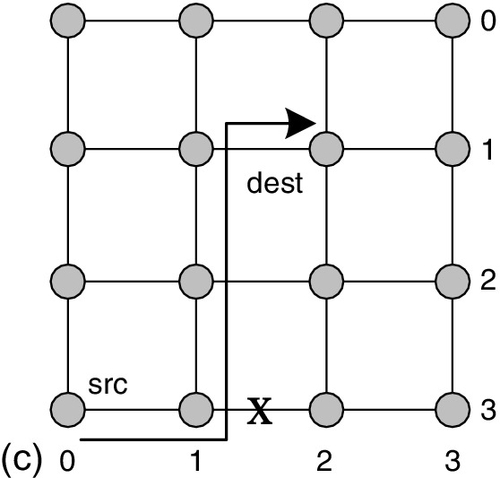
The routing algorithms can be divided into deterministic routing and nondeterministic routing on the basis of the path count provided. Deterministic routing offers only one path for each source and destination node pair. Dimensional order routing (DOR) is a typical deterministic routing algorithm. As shown in Figure 1.5a, the XY DOR offers only one path between nodes (3,0) and (1,2); the packet is firstly forwarded along the X direction to the destination's X position, and then it is forwarded along the Y direction to the destination node.

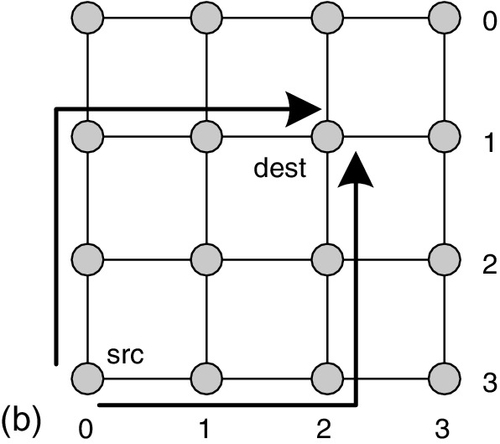
In contrast, nondeterministic routing may offer more than one path. According to whether it considers the network status, nondeterministic routing can be classified as oblivious routing or adaptive routing. Oblivious routing does not consider the network status when calculating the routing paths. As shown in Figure 1.5b, O1Turn routing is an oblivious routing algorithm [132]. It offers two paths for each source and destination pair: one is the XY DOR path, and the other one is the YX DOR path. The injected packet randomly chooses one of them. Adaptive routing considers the network status when calculating the routing paths. As shown in Figure 1.5c, if the algorithm detects there is congestion between nodes (3,1) and (3,2), adaptive routing tries to avoid the congestion by forwarding the packet to node (2,1) rather than node (3,2). Adaptive routing has some abilities to avoid network congestion; thus, it generally supports higher saturation throughput than deterministic routing.
One critical issue of the routing algorithm design is to achieve deadlock freedom. Deadlock freedom requires that there is no cyclic dependency among the network resources, typically the buffers and channels [24, 32]. Some proposals eliminate the cyclic resource dependency by forbidding certain turns for packet routing [20, 43, 46]. These routing algorithms are generally classified as partially adaptive routing since they do not allow the packets to utilize all the paths between the source and the destination. Other proposals [32, 33, 97, 99], named fully adaptive routing, allow the packet to utilize all minimal paths between the source and the destination. They achieve deadlock freedom by utilizing the VCs [24] to form acyclic dependency graphs for routing subfunctions, which act as the backup deadlock-free guarantee.
1.3.3 Flow control
Flow control allocates the network resources, such as the channel bandwidth, buffer capacity, and control state, to traversing packets. Store-and-forward (SAF) [26], virtual cut-through (VCT) [72], and wormhole [27] flow control are three primary flow control types.
Only after receiving the entire packet does the SAF flow control apply the buffers and channels of the next hop. Figure 1.6a illustrates an SAF example, where a five-flit packet is routed from router 0 to router 4. At each hop, the packet is forwarded only after receiving all five flits. Thus, SAF flow control induces serialization latency at each packet-forwarding hop.

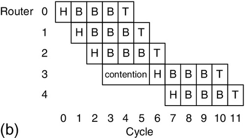
To reduce serialization latency, VCT flow control applies the buffers and channels of the next hop after receiving the header flit of a packet, as shown in Figure 1.6b. There is no contention at router 1, router 2, and router 3; thus, these routers forward the packets immediately after receiving the header flit. VCT flow control allocates the buffers and channels at the packet granularity; it needs the downstream router to have enough buffers for the entire packet before forwarding the header flit. In cycle 3 in Figure 1.6b, there are only two buffer slots at router 3, which is not enough for the five-flit packet. Thus, the packet waits at router 3 for three more cycles to be forwarded. VCT flow control requires the input port to have enough buffers for an entire packet.
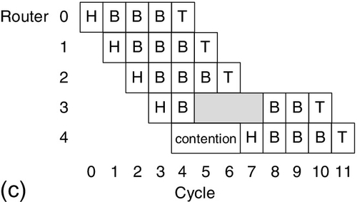
In contrast to the SAF and VCT mechanisms, the wormhole flow control allocates the buffers at the flit granularity. It can send out the packet even if there is only one buffer slot downstream. When there is no network congestion, wormhole flow control performs the same as VCT flow control, as illustrated for routers 0, 1, and 2 in Figure 1.6b and c. However, when congestion occurs, VCT and wormhole flow control perform differently. Wormhole flow control requires only one empty downstream slot. Thus, as shown in Figure 1.6c, router 2 can send out the head flit and the first body flit at cycle 3, even if the two free buffer slots at router 3 are not enough for the entire packet. Wormhole flow control allocates the channels at the packet granularity. Although the channel between routers 2 and 3 is free from cycle 5 to cycle 7 in Figure 1.6c, this channel cannot be allocated to other packets until the tail flit of the last packet is sent out at cycle 10.
The VC techniques [24] can be combined with all three flow control types. A VC is an independent FIFO buffer queue. The VC can achieve many design purposes, including mitigating the head-of-line blocking and improving the physical channel utilization for wormhole flow control, avoiding the deadlock and supporting the quality of service (QoS). For example, to improve the physical channel utilization, multiple VCs can be configured to share the same physical channel to allow packets to bypass the current blocked packet. The router allocates the link bandwidth to different VCs and packets at the flit granularity. When the downstream VC for one packet does not have enough buffers, other packets can still use the physical channel through other VCs. Table 1.1 summarizes the properties of these flow control techniques [35].
Table 1.1
Summary of Flow Control Mechanisms
| Flow Control | Channel | Buffer | Descriptions |
| SAF | Packet | Packet | The head flit must wait for the arrival of the entire packet before proceeding to the next link |
| VCT | Packet | Packet | The head flit can begin the next link traversal before the tail arrives at the current node |
| Wormhole | Packet | Flit | The channel is allocated on the packet granularity |
| VC | Flit | Flit | Can interleave flits of different packets on links |

1.3.4 Router microarchitecture
The router microarchitecture directly determines the router delay, area overhead, and power consumption. Figure 1.7 illustrates the structure of a canonical VC NoC router. The router has five ports, with one port for each direction of a 2D mesh network and another port for the local node. A canonical NoC router is mainly composed of the input units, routing computation (RC) logic, VC allocator, switch allocator, crossbar, and output units [26]. The features and functionality of these components are as follows:

• Input unit. The input unit consists of the input buffer and the related link control logic. The input buffer is built by SRAM cells or registers. The buffer slots are organized into several queues, and each queue is one VC. The queue has a circular or linked structure, with dynamically managed head and tail pointers.
• RC unit. If the flit currently at the VC head is a head flit, the RC logic calculates the output path for this packet. The calculation is performed on the basis of the destination location carried by the head flit, and it produces the output port(s) and output VC(s) for the packet. Different routing algorithms can provide different numbers of ports and VCs. The RC results may be one output VC of a particular port, or multiple or all VCs of a particular port, or multiple VCs of multiple ports. The RC result affects the implementation complexity of the VC allocator and switch allocator.
• VC allocator. After the RC has finished, the head flit requests the output VCs. The VC allocator collects the requests from all input VCs, and then allocates the output VCs to the requesting input VCs. It guarantees that one output VC is allocated at most to one input VC, and each input VC is granted at most one output VC. The requesting input VCs without getting the grants will request the VC allocation (VA) again in the next cycle. The RC and VA are performed at the packet granularity. Only the head flit conducts these two stages.
• Switch allocator. When the input VC has been successfully allocated an output VC, the router will check whether the granted downstream VC has buffers available. If it does, the flit requests the switch traversal (ST) from the switch allocator. Similarly to the VC allocator, the switch allocator guarantees each switch output port is allocated to at most one flit. The switch allocator also generates control signals to connect the input port and the output port of the crossbar. Both the VC allocator and the switch allocator consist of several arbiters. To reduce the area and power consumption, these arbiters are generally simple round-robin arbiters [26, 35] or matrix arbiters [26, 35].
• Crossbar. The crossbar is generally implemented with multiple multiplexers. The control signals for these multiplexers are generated by the switch allocator. The area and power consumption of the crossbar can be roughly modeled as O((pw)2), where p is the port count and w is the port width. Once a flit has passed the ST stage, the crossbar generates a credit to inform the upstream router of the release of a buffer slot.
• Output unit. The output unit tracks the status of downstream VCs with several registers. The “input_vc” register records the input VC that a downstream VC is allocated to. When the value of the 1-bit “idle” register is “TRUE,” the downstream VC receives the tail flit of the last allocated packet, and it is now available for reallocation to other packets. The “credits” register records the credit amount.
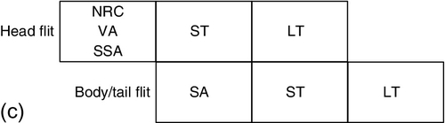
The canonical NoC router has a four-stage pipeline, as shown in Figure 1.8a. When the head flit arrives, it firstly performs the RC, and then applies the VA. After the head flit has been granted an output VC, it performs the switch allocation (SA). Finally, the flit passes the ST stage to move out of the router. The flit needs an additional link traversal (LT) stage before arriving at the next router. The body and tail flits do not pass through the RC and VA stages, and they inherit the output port and VC from the head flit.
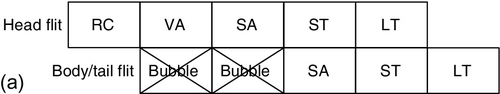
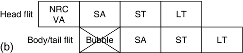
Several optimization techniques are proposed to reduce router latency. One example is the lookahead routing computation [44] shown in Figure 1.8b. Lookahead routing calculates the output port for the next router at the current router. This pipeline optimization technique can be combined with both deterministic routing and adaptive routing [78]. The head flit undergoes the next-hop routing computation in parallel with the current-hop VA, thus reducing the number of pipeline stages by one.
The speculative design is another pipeline optimization method [119]. Figure 1.8c illustrates the pipeline for the speculative SA router. The head flit undergoes speculative SA when the next-hop routing computation and VA are performed. The speculative SA assumes the head flit can get the VA grant. If this assumption is not correct, the speculative SA result is nullified, and the head flit undergoes normal SA at the next cycle. Speculative SA is very efficient with low network loads, since the VA contention is rare and most VA result assumptions are correct. With increasing network loads, the accuracy of speculative SA decreases. A more aggressive speculative design proposes speculatively performing the ST; it performs the VA, SA, and ST in parallel [112]. This aggressive speculative design achieves performance improvement only with very low network loads.
1.3.5 Performance metric
The network capacity and latency are two common performance metrics used for NoC evaluation [26, 35]. The network capacity is defined as the injection bandwidth offered to each of the N terminal nodes for uniform random traffic [9, 26]. It can be calculated from the bisection bandwidth (BB) or the bisection channel count (BC) and the channel bandwidth (b) as follows:
Since global wiring requirements depend on the channel bisection, Equation (1.1) expresses a tradeoff between NoC performance and the implementation overhead and complexity. Typically, designers desire an NoC with high network capacity. The modern CMOS technology supports a high bisection bandwidth or a large bisection channel count.
The average contention-free latency T0 from source s to destination d depends on several parameters, including the average hop count (H) from s to d and the router traversal latency (tr), which determine the routing latency; the channel traversal latency (Tc); and the packet length (L) and channel bandwidth (b), which determine the serialization latency (![]() ) [9]. The contention-free latency T0 is calculated as
) [9]. The contention-free latency T0 is calculated as
As the network load increases, greater resource contention contributes to longer router traversal latencies [26, 35]. The network latency versus injection bandwidth relationship generally exhibits a trend similar to the exponential curve, as shown in Figure 1.9. The zero-load latency is the average contention-free latency shown in Equation (1.2). The saturation throughput is defined as the injection bandwidth when the network is saturated. As shown in Figure 1.9, an obvious phenomenon for the saturated network is the sharply increased average network latency. Thus, the saturation throughput is generally measured as the injection bandwidth at which the average latency is three times the zero-load latency [95–97, 100].

1.4 Review of NoC research
In this section, we review the current research progress on several aspects of NoC design, including the topology, unicast routing, supporting collective communications, flow control, and router microarchitecture.
1.4.1 Research on topologies
Reducing the network latency is the first important research direction for topology design. Balfour and Dally [9] evaluated several topologies for on-chip communications. They point out that concentrating multiple cores into one router is an efficient way to reduce the network latency. Adding physical express channels to connect nonneighboring routers can further reduce the network latency. The concentration and physical express channels add ports to the router, improving the implementation complexity and may reduce the frequency [86]. Kim et al. [77] leveraged the off-chip flattened butterfly topology into the design of on-chip networks (OCNs). The flattened butterfly provides full connection along each dimension, and it efficiently utilizes the abundant on-chip wiring resources to reduce the network latency. The long channels in the flattened butterfly add complexities to the flow control scheme and the wiring procedure.
Improving the network saturation throughput is the second important research aspect for topology design. Mishra et al. [107] observed that the center portions of mesh networks are easily congested, which limits the saturation throughput. Thus, they propose a heterogeneous mesh network, which assigns higher bandwidth to center routers. This heterogeneous network needs to combine several small packets on narrow channels into big packets for wide channels. And it also needs to divide one large packet into several small packets for traversing narrow channels. Manevich et al. [101] combined the bus structure and the mesh network to improve the saturation throughput; the bus structure is utilized for local communication and the mesh network is leveraged for global communication.
Reducing the area and power overhead is the third important research field for topology design. Cho et al. [21] suggested adaptively adjusting the direction for each channel to improve the network throughput. Hesse et al. [55] presented a fine-grained bandwidth adaptivity mechanism based on bidirectional channels. Compared with a baseline design, their design achieves similar performance with half of the channel resources. By combining ring and mesh networks, Zafar et al. [148] proposed the cubic ring topology, which supports dynamically shutting off 30% of routers to reduce power consumption. Chen and Pinkston [17] added a ring into the baseline mesh network. The ring acts as a backup connected network when mesh routers are powered off. Their design allows all mesh routers to be shut off.
Our group conducts research on topology design. Huang et al. [64] proposed a virtual bus network which dynamically reconfigures links between routers to form the bus structure to reduce network latency. On the basis of the virtual bus structure, Huang et al. [63] further designed a hierarchical cache coherence protocol; the virtual bus delivers the local communication generated by a snoopy protocol, and the mesh network delivers the global communication generated by a directory protocol.
1.4.2 Research on unicast routing
Guaranteeing deadlock freedom and achieving high performance are two primary objectives for unicast routing designs. Designing the routing algorithm based on some deadlock avoidance theories is the general way to guarantee deadlock freedom. Dally and Seitz [24] proposed the seminal deadlock avoidance theory, which declares that an acyclic channel dependency graph is the sufficient condition for deadlock freedom. This theory can be used to design deterministic or partially adaptive routing algorithms.
Duato [32–34] introduced the concept of the routing subfunction, and indicated that a routing subfunction with an acyclic channel dependency graph is the sufficient condition for deadlock-free fully adaptive routing. Duato's theory was a great breakthrough; it allows the cyclic channel dependency for high routing flexibility. This theory has been widely used for about 20 years in several industrial products, including the Cray T3E [129] and IBM Blue Gene series [1, 16]. Duato's theory requires each VC to hold at most one packet for wormhole fully adaptive routing. Since most NoC packets are short, this requirement strongly limits the performance.
Our group conducts research to address the limitation of Duato's theory. Ma et al. [97] proposed the whole packet forwarding (WPF) flow control scheme, which extends Duato's theory to allow multiple packets to be stored in one VC. Ma et al. proved the deadlock-free property of the WPF scheme, which was also verified by Verbeek and Schmaltz [142] with the decision procedure method. Ma et al. [99] further proved that the escape VCs in Duato's theory can apply aggressive VC reallocation without inducing deadlock, which can further improve the performance.
Achieving high performance requires the routing algorithm to provide high path diversity and to avoid network congestion. The fully adaptive routing allows the packet to use all minimal paths between the source and destination nodes; thus, it supports higher path diversity than partially adaptive and deterministic routing [98]. Kim et al. [78] proposed a fully adaptive routing algorithm which utilizes lookahead routing and the port preselection scheme for low latency. Lookahead routing calculates at most two available output ports one hop ahead, and then the preselection scheme selects the appropriate port one cycle before the arrival of the packet. Hu and Marculescu [61] proposed the DyAD design, which adaptively applies deterministic or adaptive routing according to the network loads.
Avoiding network congestion requires routing algorithms to be efficiently aware of network status. The DyXY design proposed by Li et al. [89] uses dedicated wires to convey neighboring router status, and then forwards packets to either the X or the Y dimension according to the congestion status. The neighbors-on-path (NoP) design proposed by Ascia et al. [8] selected the output port on the basis of the status of routers next to neighboring routers. The NoP design leverages a sideband network to deliver congestion status for two-hop-away routers. Gratz et al. [47] proposed the regional congestion awareness (RCA) design to select the output port on the basis of the status of all routers along the same column or row. Similarly to the NoP design, a dedicated congestion information network is leveraged. When multiple applications run concurrently on a many-core platform, RCA considers the status of nodes belonging to other applications, which couples the behaviors of different applications, and negatively affects the application performance [95].
Our group conducts research to address RCA's limitations. Ma et al. [95] proposed destination-based adaptive routing (DBAR) to integrate destination locations into port selection procedures; DBAR provides dynamic isolation for concurrent applications. Ma et al. [98] further extended the DBAR design to other topologies, such as the concentrated mesh.
1.4.3 Research on supporting collective communications
Collective communications, including multicast and reduction communications, easily become the system bottleneck. There has been much research on supporting multicast communication. Lu et al. [93] proposed a path-based multicast routing design. The design first sends out the path establishment request; after receiving acknowledgment messages (ACKs) from destinations, it then sends out multicast packets. The path-based multicast routing induces path establishment and acknowledgment delays, reducing the performance.
Tree-based multicast routing eliminates path establishment and acknowledgment delays. The virtual circuit tree multicasting proposed by Enright Jerger et al. [37] introduces the concept of a virtual multicast tree. It sends out multicast packets after building up a virtual multicast tree. The building up procedure results in some overheads. To mitigate these overheads, the recursive partitioning multicast (RPM) proposed by Wang et al. [144] builds up the tree during transmission. To avoid deadlock, RPM leverages two dedicated virtual networks for upward and downward multicast packets. These two virtual networks cause unbalanced buffer utilization and reduce saturation throughput. The bLBDR design proposed by Rodrigo et al. [126] uses broadcasting in a small region for multicast communications. The broadcasting causes redundant communications. The Whirl multicast proposed by Krishna et al. [82] can efficiently support broadcasting and dense multicasting with optimized one-cycle-delay routers.
Our group researches supporting multicast communication. The virtual bus structure proposed by Huang et al. can support multicast/broadcast operations in the message passing interface (MPI) [62] and cache-coherent communications [63]. To address the unbalanced buffer utilization in the RPM design, Ma et al. [96] proposed balanced, adaptive multicast (BAM) routing. On the basis of the observation that multicast packets in cache-coherent NoCs are single-flit packets, BAM extends Duato's theory [32] for unicast routing to the design of deadlock-free multicast routing. It achieves balanced buffer utilization between different dimensions, and supports efficient bandwidth utilization through a heuristic port selection strategy.
Currently, there is little research on the support of reduction communication in NoCs. Bolotin et al. [13] noticed that combining ACKs of the cache line invalidation message may improve the performance, but they do not offer a detailed design or evaluation. Krishna et al. [82] proposed combining the ACKs at the NoCs to reduce the network load. The design keeps the earlier-arriving ACKs at the input VCs, and then combines them with the later-arriving ACKs. The earlier-arriving ACKs occupy the input VCs, which limits the performance. To mitigate this effect, Krishna et al. employed a dedicated virtual network with 12 VCs to deliver ACKs. Our group researches the support of reduction communication. The message combination framework proposed by Ma et al. [96] adds a message combination framework table to each router to support ACK combination. This design does not keep earlier-arriving ACKs inside input VCs, thus reducing the number of VCs required.
1.4.4 Research on flow control
Bufferless flow control is the first research aspect for flow control designs. The BLESS design proposed by Moscibroda et al. [109] performs RC at the flit granularity. When multiple flits contend for one port, only one flit is granted the port, and the other flits are misrouted. In contrast, the SCARAB design proposed by Hayenga et al. [51] drops the nongranted flits, and sends a negative ACK back to the source node to inform the retransmission. Jafri et al. [68] presented an adaptive flow control combining buffered and bufferless schemes that is based on a normal buffered router. The low-load routers turn off buffers to save power and apply bufferless flow control, while high-load routers apply buffered flow control. Fallin et al. [39] optimized the BLESS design in three aspects. First, they used a permutation network to implement allocators, reducing critical path delays. Second, they introduced a golden packet to avoid the livelock. The golden packet is the packet with the highest priority, and it cannot be misrouted. Third, they leveraged miss status holding registers as reordering buffers, thus reducing the required buffer amount. On the basis of this work, Fallin et al. [40] further proposed the MinBD design, which adds a side buffer to baseline bufferless routers, thus improving the network saturation throughput.
Reducing the packet transmission latency is the second research aspect for flow control designs. The flit reservation flow control proposed by Peh and Dally [118] eliminates the buffer usage limitation induced by credit round-trip delays. The express VC proposed by Kumar et al. [85] reduces latencies by preallocating buffers of multiple routers. On the basis of this work, Kumar et al. [84] further proposed token flow control, which broadcasts the current buffer occupation status to nearby routers. Then, the packet forwarding can bypass the pipeline of several routers. The layered switching design proposed by Lu et al. [92] divides the long packet into several flit groups. It maintains SA results for an entire flit group to reduce contention and latencies. Enright Jerger et al. [36] proposed hybrid circuit switching to combine the circuit switching and packet switching mechanisms. The wormhole cut-through design presented by Samman et al. [127] allows several packets to be mixed in one VC at the flit granularity.
Avoiding deadlock for ring/torus networks is the third research aspect of flow control designs. Bubble flow control (BFC) avoids deadlock by prohibiting occupation of the last free packet-size buffers [15, 122, 123]. On the basis of the BFC scheme, Chen et al. [19] proposed the critical bubble scheme (CBS); this scheme achieves deadlock freedom by marking one bubble inside the ring as the critical one, and this critical bubble can be occupied only by packets traveling inside the ring. On the basis of the CBS design, Chen and Pinkston [18] further proposed worm bubble flow control (WBFC), which extends the BFC idea to wormhole networks. It assigns to the buffers three different colors to convey the global buffer utilization status into local information and to avoid starvation. WBFC allows the ring to leave only one free flit-size buffer to avoid deadlock for wormhole networks. The prevention flow control proposed by Joshi et al. [69] combines the priority arbitration and prevention slot cycling scheme to avoid deadlock. The priority arbitration gives higher priority to already injected packets, and the prevention slot cycling scheme keeps one free packet-size buffer inside the ring. Luo and Xiang [94] proposed a fully adaptive routing with only two VCs for torus networks. Their design allocates VCs according to whether the packet needs to cross wraparound links in the future.
Our group researches flow control designs. On the basis of the observation of the inefficiency of BFC, CBS, and prevention flow control in handling variable-sized packets, Ma et al. [100] proposed flit bubble flow control (FBFC). The kernel idea of FBFC is similar to that of WBFC. By maintaining one free flit-size buffer inside the ring, FBFC achieves deadlock freedom for wormhole ring/torus networks. FBFC implementations can be regarded as a hybrid flow control; the packet injection is similar to VCT flow control, and the packet movement follows wormhole flow control.
1.4.5 Research on router microarchitecture
Reducing the number of pipeline stages is the first aspect of router design. Peh and Daily [119] proposed speculative SA to reduce the number of pipeline stages by one; their design speculatively performs SA in parallel with VA. Mullins et al. [112] further used the speculative ST to reduce the number of stages by one more. Their design allows the packet to go straight into the ST under low loads. Matsutani et al. [104] evaluated the performance of several different prediction algorithms. The speculative SA and ST need an additional switch allocator, increasing the router complexity. On the basis of priority allocation, Kim [76] proposed a low-cost router for DOR. It simplifies the router into two multiplexers and a few buffers. To support low-latency transmission, the router assigns higher priorities to straight-traveling packets than to turning ones. Recently, Kim et al. [75] extended this low-cost router to hierarchical ring networks. Hayenga and Lipasti [52] observed that most NoC packets are short packets, and they creatively leveraged the property of XOR logic into NoC router designs. Their proposed NoX router eliminates one pipeline stage, while it does not induce additional switch allocators. The NoX router needs additional effort to handle long packets. Our group researches low-latency routers. By adding directly connecting channels between input and output ports, Lai et al. [87] implemented a low-cost single-cycle router.
Reducing the buffer overhead is the second aspect for router design. The dynamically allocated multiqueue (DAMQ) buffer [136] is an efficient way to reduce buffer amount requirements. The ViChaR design proposed by Nicopoulos et al. [113] introduced the DAMQ buffer into the NoC buffer design, and it achieves obvious area and power improvements. Xu et al. [147] noticed the ViChaR structure needs too many VCs, which limits the frequencies. Thus, they proposed a DAMQ structure with limited and constant VCs. Ramanujam et al. [124] implemented a distributed buffer to achieve the performance of the output buffer, while avoiding the overhead of the output buffer. Their design configures both input buffers and DAMQ-style center buffers in NoC routers. Ahmadinia et al. [4] proposed a DAMQ buffer to share buffers among different physical ports. Becker et al. [10] observed that previous DAMQ buffer designs cannot support QoS efficiently; thus, they proposed a DAMQ buffer design which assigns a minimum number of buffers to each VC to provide QoS support. The elastic buffer proposed by Michelogiannakis et al. [106] utilizes flip-flops inside long channels and routers as buffers, thus removing router input buffers. Kodi et al. [80] used repeaters inside channels as buffers, which reduces the input buffer amount. Kim et al. [74] observed that most buffers are idle during the application running period; thus, they applied fine-grained power-gating techniques to control the status of each buffer slot to reduce power consumption.
Our group researches buffer design. Lai et al. [88] proposed a DAMQ buffer design which can efficiently avoid network congestion. Their research supports sharing buffers among different VCs of the same physical port. Shi et al. [133] further proposed a DAMQ buffer to support sharing buffers among different physical ports.
1.5 Trends of real processors
In this section, we discuss the NoC design trends for several commercial or prototype processors, including the MIT Raw, Tilera TILE64, Sony/Toshiba/IBM Cell, U.T. Austin TRIPS, Intel Teraflops, Intel SCC, Intel Larrabee, and Intel Knights Corner processors.
1.5.1 The MIT Raw processor
MIT has developed the Raw processor since the late 1990s to address several emerging design challenges, including internal wire lengths being increasingly limited by the scaling frequency, market constraints for quickly verifying new designs, and applications emphasizing stream-based multimedia computations [137]. The kernel design idea of the Raw processor is to keep the hardware simple and leave most performance-scaling jobs to the software. The Raw processor has 16 tiles, and each tile can execute instructions independently. There is an eight-stage MIPS-like processing core, a 32 kB data cache, and a 96 kB instruction cache on each tile. It also has static and dynamic routers for static and dynamic communications respectively. The Raw processor is manufactured with IBM's SA-27E, 0.15-μm, six-level, copper, application-specific integrated circuit (ASIC) process. Its design target is a 225 MHz worst-case frequency.
As illustrated in Figure 1.10, the 16 tiles are organized in a 4 × 4 mesh topology. The Raw processor has two static networks and two dynamic networks. The static and dynamic networks both have a 32-bit physical channel width. Both static and dynamic networks are register mapped directly into the bypass path of the processing core; the core loads or stores registers R24 and R25 to access two static networks. Dynamic networks are mapped to registers R26 and R27. Static network configurations are scheduled at compile time. On the basis of the compiled instructions, static routers can collectively reconfigure the entire communication pattern of the static network on a cycle-by-cycle basis. Since the static router knows the packet destination long before the packet arrives, it performs preconfigurations to allow packets that have arrived to be delivered immediately. The per-hop latency of static networks is one cycle. This low-latency property is critical for efficiently bypassing scalar operands to exploit instruction-level parallelism.

In contrast, the packets in dynamic networks are generated and routed according to computational results during the run time. Thus, dynamic routers have more latency than static routers as they have to wait for the arrival of the header flit to initiate router configurations. The dynamic network applies DOR. Its per-hop latency is one cycle for straight-traveling packets and two cycles for turning packets. The dynamic network applies credit-based wormhole flow control. Although DOR eliminates the network-level deadlock, dynamic networks still need to consider the protocol-level deadlock. The two dynamic networks apply different schemes to handle the protocol-level deadlock. The memory network applies the deadlock avoidance scheme on the basis of resource usage limitations. The general network applies the deadlock recovery scheme, which uses the memory network as backup deadlock-free delivery paths.
1.5.2 The Tilera TILE64 processor
Tilera's TILE64 processor is a commercial product inspired by the MIT Raw processor [145]. The TILE64 processor is a general-purpose many-core processor, which mainly focuses on multimedia, networking, and wireless applications. It has a multiple instruction, multiple data (MIMD) architecture with 64 cores arranged in an 8 × 8 tiled mesh topology. Each tile has a three-way very long instruction word core with an independent program counter, a two-level cache hierarchy with 768 kB capacity, a 2D direct memory access (DMA) subsystem to exchange data among cores and memory controllers, and a switch to interconnect neighboring tiles. Each tile is a fully featured computing system which can independently run the Linux operating system. Also, multiple tiles can be combined to run a multiprocessor operating system, such as SMP Linux. To optimize the power consumption, the TILE64 processor employs extensive clock gating and applies power gating on the tile granularity.
The TILE64 processor is implemented in 90 nm technology, with a frequency up to 1 GHz. It can perform 192 billion 32-bit operations per second. The TILE64 processor supports subword arithmetic and can achieve 256 billion 16-bit operations per second, or half a teraops for 8-bit operations. To facilitate programming, the TILE64 processor provides a communication library, iLib, based on the C programming language. The iLib library supports two communication types, the socket-like streaming channel and the MPI-like communication API. The socket channel supports higher performance than the MPI, while its flexibility is poorer than that of the MPI.
The TILE64 processor employs five physical networks, including one static network and four dynamic networks, as shown in Figure 1.11. Similarly to the Raw processor, the connections of the static and dynamic networks are configured at compile time and run time respectively. Each of the five physical networks has a 32-bit channel width. The static network applies circuit switching flow control, with a per-hop latency of one cycle. The dynamic network leverages DOR with wormhole flow control. Each input port has the minimal three buffer slots to cover the credit round-trip delay. The per-hop latency for straight packets is one cycle, while it is two cycles for turning packets.

The four dynamic networks serve different purposes. The user dynamic network delivers communications for userland processes or threads. The input/output dynamic network transfers traffic between input/output devices and processing tiles. It also serves for operating-system and hypervisor-level communications. The memory dynamic network exchanges data between on-tile caches and off-chip DRAMs. The tile dynamic network works in concert with the memory dynamic network as a portion of the memory system. The request packets of direct tile-to-tile cache transfers transit the tile dynamic network, and responses transit the memory dynamic network. This avoids protocol-level deadlock for the tile dynamic network. The memory dynamic network uses the buffer preallocation scheme to avoid protocol-level deadlock. It reserves certain buffers at memory controllers for each cache block. The input/output dynamic network and the user dynamic network leverage deadlock recovery mechanisms to handle protocol-level deadlock. They use the off-chip DRAM as the backup memory space in case of deadlock.
To support the virtualization and protection among concurrent applications or supervisors, the TILE64 processor provides Multicore Hardwall technology. This technology protects links on the user-accessible user dynamic network, input/output dynamic network, and static network, while the memory dynamic network and the tile dynamic network are protected by memory protection mechanisms through a translation lookaside buffer. If a packet attempts to cross a hardwalled link, the Multicore Hardwall blocks the packet and triggers an interrupt to system software to take appropriate actions.
1.5.3 The Sony/Toshiba/IBM cell processor
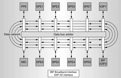
The Sony/Toshiba/IBM Cell Broadband Engine is developed primarily for multimedia applications and scientific computations. It has a heterogeneous architecture with 12 core elements connected through a multiring bus called an element interconnect bus (EIB) [5, 71, 79], as shown in Figure 1.12. The elements include one controlling core called a power processing element (PPE), eight computation cores called synergistic processing elements (SPEs), one memory interface controller (MIC), and two bus controllers (IOIF0, IOIF1).
The dual-threaded PPE is a complete 64-bit IBM Power Architecture processor featuring a 32 kB first-level (L1) cache and a 512 kB second-level (L2) cache, and it can run the operating system. The SPEs are 128-bit single instruction, multiple data (SIMD) processing units optimized for data-rich workloads allocated to them by the PPE. Each SPE contains 256 kB of local store memory. The PPE supports both DMA and memory-mapped input/output, while DMA is the only method for moving data between the SPE's local store and the system memory. The Cell processor is implemented in 90 nm silicon-on-insulator technology. The SPE and the PPE run at a frequency of 3.2 GHz, and the EIB operates at 1.6 GHz.
The EIB supports communications among 12 elements. All elements contain bus interface units to access the EIB, and each element is capable of an aggregate throughput of 51.2 GB/s. Thus, the data rate requirement of the EIB is quite high. Also, the EIB needs to efficiently handle coherent data transfers whose packet size may vary. The EIB architecture is optimized to satisfy the above requirements.
The EIB has independent networks for commands (requests for data from other sources) and for the data being moved. It consists of a shared command bus, four 128-bit data rings (two in each direction), and a central data arbiter. The command bus distributes commands, sets end-to-end transactions, and handles memory coherence. It consists of five distributed address concentrators arranged in a treelike structure that lets multiple commands be outstanding simultaneously across the network. The address concentrators handle collision detection and prevention, and they provide fair access to the command bus by a round-robin mechanism. All address concentrators forward commands to a single serial command reflection point.
The data transfer is elaborate. Each of the four data rings can handle up to three concurrent nonoverlapping transfers, allowing the EIB to support 12 concurrent data transfers. The data ring applies slotted ring flow control and shortest path routing. The central data arbiter coordinates the accesses for data rings on a per transaction basis. It implements round-robin arbitration with two priority levels. The MIC has the highest priority for the data arbiter, while all other elements have a lower priority.
1.5.4 The U.T. Austin TRIPS processor
The TRIPS processor is an academia prototype developed by the University of Texas at Austin [48]. It is a distributed processing system consisting of multiple tiles connected via multiple NoCs. The TRIPS processor applies an explicit data graph execution (EDGE) architecture, where the computation is driven by the data arrival [49]. The TRIPS processor contains two out-of-order cores, and each core has 16 execution units, a 32 kB L1 data cache and a 64 kB L1 instruction cache. Since each execution unit can independently execute instructions, the TRIPS core can simultaneously issue 16 instructions in the out-of-order fashion. The processor also integrates a 1 MB static nonuniform cache architecture L2 cache. The TRIPS chip is implemented with the IBM CU-11 ASIC process, with a drawn feature size of 130 nm and seven layers of metal. Its work frequency is 366 MHz.
As illustrated in Figure 1.13, the TRIPS processor applies a tiled structure; the L2 cache and the processing cores, including the execution units, register files, and L1 data/instruction caches are divided into 106 tiles. Leveraging one NoC to connect all 106 tiles is a possible design choice. Yet, to achieve high performance and resource efficiency, the TRIPS processor leverages two customized types of NoCs to connect core elements and the L2 memory system respectively. The operand network (OPN) connects 25 core element tiles with a 5 × 5 mesh topology, and it replaces the traditional operand bypass bus and L1 cache bus. The OPN-connected nodes include 16 execution tiles, four register file tiles, four L1 data cache tiles, and one global control tile. The remaining five L1 instruction tiles are connected with special control networks and managed by the global control tile to implement the block execution of the EDGE architecture [49].
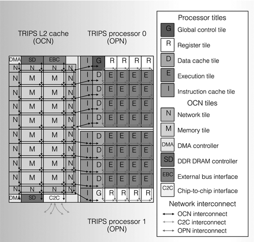
The block execution model preallocates reservation stations for operands. Thus, the OPN does not need to handle protocol-level deadlock. It uses only one VC with four buffer slots. The OPN has a 142-bit physical channel width, including 4 bits for flow control, 29 bits for control physical digits, and 109 bits for data payloads. This physical channel width is chosen to make all operand packets delivered in the OPN be single-flit packets. The OPN utilizes YX DOR, with wormhole flow control based on the on/off mechanism. There are two 5 × 5 crossbars inside each OPN router: one crossbar is for data payloads and the other one is for the control physical digits. The control physical digits, including the destination node and instructions, are sent one cycle before the data payload to preconfigure the data payload crossbar. The per-hop latency of the OPN is one cycle.
The on-chip network (OCN) connects the 40 on-chip memory system tiles with a 4 × 10 mesh topology, and it replaces the traditional memory bus. The 40 tiles include 16 memory tiles and 24 network tiles. In addition to the four-way, 64 kB memory bank, each memory tile also includes an OCN router and a single-entry miss status holding register. The memory bank can be configured as an L2 cache bank or as a scratch-pad memory, with configuration commands from cores. The network tiles surrounding the memory tiles act as translation agents for determining where to route memory requests. Each network tile contains a programmable routing table to determine the request destinations.
The OCN leverages four virtual networks to avoid protocol-level deadlock, and each virtual network has one VC with two buffer slots. The OCN has a 138-bit physical channel width, with 128-bit payloads and 10-bit flow control signals. This channel width is chosen as it is the closest even divisor of a cache line size that would allow the small memory request packets to fit in one flit. The OPN packet lengths range between one flit and five flits. The OCN applies the YX DOR with credit-based wormhole flow control. It has a one-cycle per-hop latency. The OCN router has a 6 × 6 crossbar. In addition to the regular five ports to connect neighboring routers and a local tile, the other port is used for configuring the local memory address translation table.
1.5.5 The intel Teraflops processor
The Teraflops processor chip is the first-generation silicon prototype of the terascale computing research initiative at Intel [140, 141]. It consists of 80 homogeneous tiles arranged in an 8 × 10 mesh topology operating at 5 GHz and 1.2 V. Each tile has a simple processing engine, with two independent, fully pipelined single-precision floating point multiply accumulators. A tile also has a 3 kB single-cycle instruction memory, a 2 kB data memory, and a five-port router. The Teraflops processor has an eight-way very long instruction word instruction set architecture. The design target for the power consumption is under 100 W when achieving a performance of more than 1 Tflop. It applies fine-grained clock gating and power gating techniques to optimize the power consumption. Each tile is partitioned into 21 sleep regions, and each of them can be dynamically controlled by special sleep/wake up instructions. The router is divided into 10 sleep regions with control of each individual port. The Teraflops chip is implemented in 65 nm technology. Its total area is 275 mm2, and each tile occupies 3 mm2.
The 8 × 10 mesh network has one 39-bit physical channel, with 32 bits for payloads, 6 bits for flow control, and 1 bit for the mesochronous communication [57]. The mesochronous communication allows neighboring routers to communicate with different clock edges, which mitigates the difficulty to design a global clock distribution network. The network has two logic lanes, and each logic lane consists of one VC with 16 buffer slots. The two logic lanes are used for the instruction and data, respectively, to avoid short instruction packets being blocked by long data packets.
The per-hop latency of the mesh network is five cycles, including the buffer write, buffer read, RC, arbitration, and ST pipeline stages, as shown in Figure 1.14. The network applies DOR with on/off-based wormhole flow control. The Teraflops processor uses source routing; the entire routing path is encoded in the head flit. Since a head flit can at most encode output ports for 10 hops, the possible remaining output ports are encoded by a chained head flit. The router arbitration utilizes a two-stage arbitration structure. The first stage performs the physical port arbitration at the packet granularity, and the second stage conducts the logic lane arbitration at the flit granularity. To reduce the area overhead, the Teraflops processor uses double-pumped crossbars. This type of crossbar leverages one crossbar wire to deliver the signals from two input wires at the high and low periods of a cycle respectively. Thus, it eliminates half of the wiring overhead for the crossbar. The entire router is implemented in 0.34 mm2.

1.5.6 The intel SCC processor
The Intel SCC processor is a prototype processor with 48 IA-32 architecture cores connected by a 6× 4 mesh network [59]. As shown in Figure 1.15, every two cores are integrated into one tile, and they are concentrated to one router. A total of four memory controllers, two on each side, are attached to two opposite sides of the mesh. The IA-32 cores are the second-generation in-order Pentium P54C cores, except that the L1 ICache/DCache capacity is upgraded from 8 to 16 kB. The L1 ICache and DCache both support four-way set associativity. They can be configured in write-through or write-back modes. Each core has a 256 kB, four-way set associative, writeback L2 cache. The L1 and L2 cache line sizes are both 32 bytes. The L2 cache is not inclusive with respect to the L1 cache. The SCC chip is implemented in 45 nm, nine-metal-layer, high-K CMOS technology. Its area is 567 mm2, and each tile's area is 18 mm2.
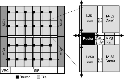
The SCC processor does not support the hardware cache coherence protocol. Instead, it uses the message passing programming paradigm, with software-managed data consistency. To support this programming paradigm, L1 DCache lines add one message passing memory type bit to identify the line content as normal memory data or message passing data. To maintain data consistency, a core initial message write or read operation must first invalidate all message passing data cache lines. Then, the cache miss forces write or read operations to access the data in the shared memory. Each tile contains a 16 kB addressable message passing buffer to reduce the shared memory access latency.
To optimize the power consumption, the SCC chip applies dynamic voltage and frequency scaling (DVFS), which adjusts the processor's voltage and frequency according to management commands. The tile's DVFS range is between 300 MHz at 700 mV and 1.3 GHz at 1.3 V, and the NoC's range is between 60 MHz at 550 mV and 2.6 GHz at 1.3 V. The nominal usage condition is 1 GHz at 1.1 V for the tile and 2 GHz at 1.1 V for the NoC. The SCC chip consists of eight voltage islands: two voltage islands supply the mesh network and die periphery, and the remaining six voltage islands supply the processing cores, with four neighboring tiles composing one voltage island. The processor contains 28 frequency islands, with one frequency island for each tile and one frequency island for the mesh network. The remaining three frequency islands serve as the system interface, voltage regulator, and memory controllers respectively.
The mesh network of the SCC processor achieves a significant improvement over the NoC of the Teraflops processor. Its physical channel width is 144 bits, with 136 bits for payloads and 8 bits for flow control. The router architecture is optimized for such a wide link width. The router has a four-stage pipeline targeting a frequency of 2 GHz. The first stage includes the LT and buffer write, and the second stage performs the switch arbitration. The third and fourth stages are the VA and the ST respectively. To improve the performance, the router leverages the wrapped wave-front allocators. The mesh network applies lookahead XY DOR with VCT flow control. Each physical port configures eight VCs. To avoid protocol-level deadlock, the SCC processor employs two virtual networks: one for the request messages and the other one for the response messages. Each virtual network reserves one VC, and the remaining six VCs are shared between the two virtual networks.
1.5.7 The intel Larrabee processor
The Larrabee processor is an Intel GPGPU, which was expected to be released in 2010 [130], but it was cancelled owing to delays and disappointing early performance figures. The Larrabee processor can be considered as a combination of a multicore CPU and a graphics processing unit (GPU), and has similarities to both. Its coherent cache hierarchy and x86 architecture compatibility are CPU-like, while its wide SIMD vector units and texture sampling hardware are GPU-like.
The Larrabee processor is based on simple in-order P54C Pentium cores, and each core supports four-way interleaved multithreading, with four copies of each processor register. The original P54C core is extended with a 512-bit vector processing unit to provide high graphic processing performance. This vector unit can perform 16 single-precision floating point operations simultaneously. Also, the processor integrates one major fixed-function graphics hardware feature: the texture sampling unit. But to provide more flexibility than current GPUs, the Larrabee processor has less specialized graphic hardware than the GPGPUs from NVIDIA and AMD.
As interconnection features, the Larrabee processor has a 1024-bit (512 bits in each direction) data ring bus for communication between cores and the memory, as shown in Figure 1.16. The network structure is similar to the ring utilized in the Nehalem-EX processor [116]. The packet routing decisions are made before injection, by selecting the ring with the minimal distance. The ring applies the polarity stop scheme. Each ring stop has an odd or even polarity, and can only pull from the appropriate ring that matches that polarity. The ring changes polarity once per clock, so which stop can read from which ring on a given cycle is easy to figure out. An injecting ring stop knows the destination ring stop and the destination stop's polarity. It also knows the hop count to the destination ring stop. Thus, the source can figure out when to send a packet so that the destination can actually read it. By introducing a delay of at most one cycle, a source can ensure the destination can read the injected packet, and the case of two packets arriving at the same time never occurs. The routing and polarity stop flow control simplify the network: since injected packets are never blocked, no storage is required in the routers.

1.5.8 The intel Knights Corner processor
The Intel Knights Corner processor (product name Xeon Phi) is a many-core processor mainly targeted at highly parallel, high-performance computing fields [22, 67]. It is manufactured with Intel's 22 nm FinFET process, and its performance is more than 1 Tflops with a frequency higher than 1 GHz. Its architecture incorporates Intel's earlier work on the development of the Larrabee [130], Teraflops [141] and SCC [59] processors. It leverages the 512-bit vector unit and ring-bus-based cache-coherent system introduced in the Larrabee processor [130], and it also uses sophisticated DVFS techniques included in the SCC processor [59]. In addition, investigation of the Teraflops processor for efficient on-chip communications [141] offers insights for the Knights Corner processor design.
The Knights Corner processor contains more than 60 cores, which are modified on the basis of the P54C core. The cores, eight GDDR5 memory controllers, and the PCI Express interfaces are connected by a ring bus. Similarly to the Larrabee core, each Knights Corner core includes a scalar pipeline and a vector pipeline. Compared with the Larrabee core, in the Knights Corner core, the vector pipeline is enhanced for high double-precision floating point performance. Each core supports four-way interleaved multithreading to alleviate memory access bottlenecks for in-order instruction executions. Each core contains a 32 kB L1 DCache and a 32 kB L1 ICache, and a 512 kB unified private L2 cache. The L1 and L2 caches both support eight-way set associativity, with 64-byte cache line sizes. The cache hierarchy maintains the inclusive property to mitigate coherent overheads. The memory system is optimized for high performance. The L1 DCache supports 64-byte read/write per cycle. Each core contains 16 stream prefetchers and a 64-entry translation lookaside buffer for the L2 cache. The L1 and L2 caches can both support up to about 38 outstanding requests per core. The streaming store instructions, which allow the cores to write an entire cache line without reading it first, are added to reduce memory bandwidth consumption. Although the L2 cache is private to each core, the tag directory on each core is shared by the whole processor.
To optimize power consumption, the Knights Corner processor implements a bunch of power management modes (the C-states in Intel's terminology). The C0 mode is full power like in CPUs, the core C1 mode clock gates one core, and the core C6 mode power gates that core but not the L2 cache. Since other cores can snoop the L2 cache, it cannot be powered down until all cores are in at least the C1 mode. The ring has the same problem: it cannot go to sleep until everything else does. When all the cores are power gated and the uncore detects no activity, the tag directories, ring bus, L2 caches, and memory controllers are clock gated. Then, the Knights Corner processor enters the Package C6 state, which powers down everything but the PCI Express interface to wait for wake-up commands from the host PC, and the GDDR5 is put into self-refresh mode.
In principle, the ring structure of the Knights Corner processor is similar to those in the Nehalem-EX [116] and Larrabee [130] processors. As illustrated in Figure 1.17, the cache coherence system leverages three kinds of rings. The main ring is the 64-byte-wide data block ring, which is able to carry a full cache line. The other two types of rings are the narrower address ring and acknowledgment ring. The address ring delivers the address and read/write commands, and the acknowledgment ring carries flow control and coherence messages. Unlike the Nehalem-EX processor, the Knights Corner processor utilizes a complex controller to allow each stop to inject a packet into the ring every clock. After injection, the packets are deterministically delivered to the destination. The Knights Corner processor allows packet bouncing; in some cases, the destination may not have space to accept the packet, and so it is left on the ring and then picked up the next time the packet goes by.
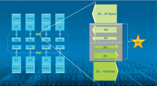
Intel has found that the address and acknowledgment rings become performance bottlenecks and exhibit poor scalability beyond 32 cores [67]. Since these rings carry almost constant-sized packets, doubling the ring widths to deliver larger packets cannot alleviate the problem. Instead, Intel doubles the number of both address and acknowledgment rings to send more packets. Thus, there are now ten rings in total, or five in each direction, as shown in Figure 1.17. This allows scaling to 60+ cores, eight memory controllers, and many other supporting ring stops like the PCI Express interface. In the physical layout of the Knights Corner processor each GDDR5 memory controller is physically associated with a fixed number of cores. Although all cores can access all memory controllers, leveraging this physical proximity to reduce ring hops is helpful for performance.
1.5.9 Summary of real processors
The NoCs of real processors have a significant design space as illustrated by the examples in the last sections. The functionalities and requirements of these NoCs are rich and different. The Raw and TRIPS processors mainly use the NoCs for operand bypassing; the NoC's low-latency property is critical for the whole processor's performance. The Cell processor primarily uses the NoC to deliver data for DMA operations, which requires high network bandwidth. The NoCs in the TILE64 and SCC processors mostly deliver data for the message passing paradigm, while the NoCs in the Larrabee and Knights Corner processors transfer cache-coherent data for the shared memory paradigm. Two independent physical networks or virtual networks are enough to avoid protocol-level deadlock for the message passing paradigm, such as the design in the SCC processor. In contrast, the complex cache coherence transaction causes the shared memory paradigm to use more physical networks or virtual networks to avoid protocol-level deadlock.
The design choices for each aspect of these NoCs span a continuum. Tables 1.2 and 1.3 list the basic NoC properties for these real chips. For processors with small numbers of cores, such as the Cell processor, the ring topology is appropriate for connection. Large numbers of cores require the more scalable 2D mesh topology, as in the TILE64, Teraflops, and SCC processors. In the Knights Corner processor a notable topology choice is made by using the ring network to connect more than 60 cores and other additional memory controllers and input/output interfaces. This processor leverages 10 rings to eliminate the performance bottleneck caused by the NoC congestion. Most real processors use the simple XY or YX DOR for 2D mesh NoCs, or shortest path routing for ring NoCs. These simple routing algorithms easily avoid network-level deadlock and require only a few hardware resources. Moreover, their low complexities are more convenient to achieve high frequencies.
Table 1.2
The Node Count, Topology, and Routing Algorithms of the NoCs for Real Chips
| Processor | No. of Nodes | Topology | Routing Algorithm |
| Raw (dynamic) | 16 | 4 × 4 mesh, two PNs. | XY DOR |
| Each PN is 32 bits wide | |||
| TILE64 (dynamic) | 64 | 8 × 8 mesh, four PNs. | XY DOR |
| Each PN is 32 bits wide | |||
| TILE64 (static) | 64 | 8 × 8 mesh, one PN with a 32-bit width | XY DOR |
| Cell | 12 | Four rings, two for each direction. | Shortest path |
| Each ring is 128 bits wide | |||
| TRIPS (OPN) | 25 | 5 × 5 mesh, one PN with a 142-bit width | YX DOR |
| TRIPS (OCN) | 40 | 4 × 10 mesh, four VNs. | YX DOR |
| 1 PN with a 138-bit width | |||
| Teraflops | 80 | 8 × 10 mesh, two VNs. | YX DOR |
| 1 PN with a 39-bit width | Source routing | ||
| SCC | 24 | 6 × 4 mesh, two VNs. | XY DOR |
| 1 PN with a 144-bit width | |||
| Larrabee | 16+ | Two data rings, one for each direction. | Shortest path |
| Each data ring is 512 bits wide | |||
| Knights Corner | 60+ | Two data rings and eight control rings. | Shortest path |
| Each direction has five rings. | Allow packet bouncing | ||
| Each data ring is 512 bits wide |
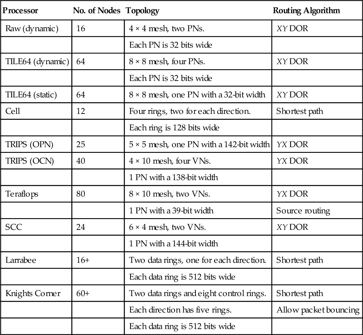
PN, physical network; VN, virtual network.
Table 1.3
The Flow Control and Per-Hop Latency of the NoCs for Real Chips
| Processor | Flow control | Per-hop latency |
| Raw (dynamic) | Wormhole, credit based | Straight: one cycle, turn: two cycles at 225 MHz (worst case), 150 nm process |
| TILE64 (dynamic) | Wormhole, credit based | Straight: one cycle, turn: two cycles at 1 GHz, 90 nm process |
| TILE64 (static) | Circuit switching | One cycle at 1 GHz, 90 nm process |
| Cell | Circuit switching | One cycle at 1.6 GHz, 90 nm process |
| TRIPS (OPN) | Wormhole, on/off based | One cycle at 366 MHz, 130 nm process |
| TRIPS (OCN) | Wormhole, credit based | One cycle at 366 MHz, 130 nm process |
| Teraflops | Wormhole, on/off based | Five cycles at 5 GHz, 65 nm process |
| SCC | Virtual cut-through | Four cycles at 2 GHz, 45 nm process |
| Larrabee | Slotted ring, polarity stops | One cycle |
| Knights Corner | Slotted ring | One cycle at 1.05 GHz, 22 nm process |
The flow control of these NoCs includes the circuit switching, slotted ring, worm-hole, and VCT mechanisms. The circuit switching flow control needs to configure a route path before sending packets; the Cell processor uses the shared command bus and data bus arbiter to build up the route path, while the TILE64 processor preconfigures the routers on the basis of compiled instructions. The Larrabee and Knights Corner processors both use slotted ring flow control, which requires all messages to be single-flit packets to fill into the ring slot. Thus, both processors have large link widths for the data ring to encode a full-size cache line. The wormhole flow control can be implemented as credit-based or on/off-based flow control. These two implementations require different minimum buffer amounts for correctness or for avoidance of buffer utilization bubbles [23]. The Raw and TILE64 processors and the OCN in the TRIPS processor use the credit-based wormhole flow control, while the Teraflops and the OPN in the TRIPS processor use the on/off-based design. Although previous research suggests that VCT flow control may not be appropriate for NoC design as it consumes large buffers [25], the SCC processor attempts to use this flow control mechanism in OCNs. Compared with wormhole flow control, VCT flow control can simplify the allocator design, thus supporting higher frequencies [59].
These NoCs are manufactured with processes ranging from the 150 nm IBM ASIC for the academia prototype Raw processor to the 22 nm trigate for the commercial Knights Corner processor. The academia prototypes, Raw and TRIPS, target relatively lower frequencies of hundreds of megahertz. The Teraflops processor is used to demonstrate highly optimized OCN design. Thus, it targets a very high frequency of 5 GHz. Its NoC's power consumption is more than 10% of the whole processor's power consumption, which exceeds Intel's expectation [57]. Intel's following processors, including the SCC, Larrabee, and Knights Corner processors, have lower frequency goals. A moderate frequency is more efficient for throughput-oriented many-core power computation [67].
1.6 Overview of the book
On the basis of the communication-centric cross-layer optimization method presented in Section 1.2, we have organized this book in five parts and 11 chapters, whose structure is illustrated in Figure 1.18. The Prologue and the Epilogue introduce and conclude this book respectively. Future work is also proposed in the Epilogue. The intermediate three parts, which consist of nine chapters, form the main content of this book. These parts describe communication-centric cross-layer optimizations for the NoC design space, in a thorough and bottom-up way.
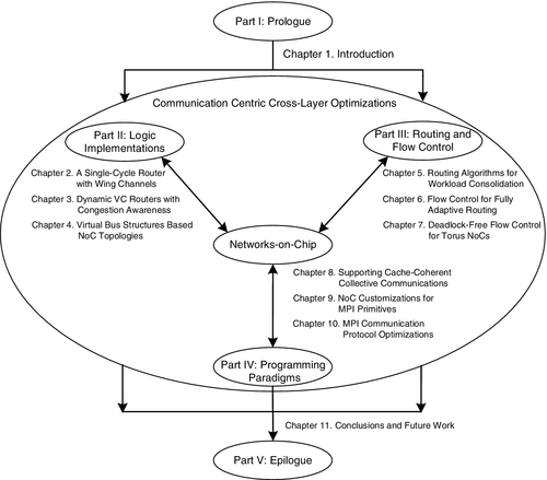
Part II, on logic implementations, focuses on the optimization of NoC logic implementations, including efficient router architecture, buffer structure, and network topology designs. It contains three chapters, Chapters 2–4. Chapter 2 proposes a low-cost single-cycle router architecture with wing channels. The wing channels forward incoming packets to free ports immediately with the inspection of SA results, thus achieving a single-cycle router delay. Moreover, the incoming packets granted wing channels can fill in the free time slots of the crossbar and reduce contention with subsequent packets, thereby improving throughput effectively. Chapter 3 discusses the design of dynamic NoC VC structures. It first introduces a DAMQ buffer structure, which can efficiently avoid network congestion. This structure adaptively adjusts the VC depth and VC amount on the basis of network loads to mitigate network blocking. Then, it presents a novel NoC router with a shared-buffer structure named a hierarchical bit-line buffer. The hierarchical bit-line buffer supports sharing buffers among different physical ports, and it assigns higher priorities to packets heading to lightly loaded ports to avoid network congestion. Chapter 4 studies a new NoC topology of incorporating buses into NoCs in order to take advantage of both NOCs and buses in a hierarchical way. The proposed virtual bus OCN dynamically uses point-to-point links of conventional NoC designs as bus transaction links to support high-performance multicast and broadcast communications.
Part III, on routing and flow control, delves into the design of high-performance NoC routing algorithms and flow control mechanisms on the basis of the traffic characteristics. There are three chapters, Chapters 5–7. In Chapter 5 a holistic approach is used to design efficient routing algorithms for workload consolidation scenarios. It proposes a novel selection strategy, the destination-based selection strategy, for adaptive routing algorithms in many-core systems running multiple concurrent applications. Its exploration considers several critical aspects of routing algorithms, including adaptivity, path selection strategy, VA, isolation, and hardware implementation cost, to ensure an efficient design. Chapter 6 mainly focuses on efficient flow control designs for deadlock-free fully adaptive routing algorithms. It presents two novel flow control designs. First, WPF reallocates a nonempty VC if the VC has enough free buffers for an entire packet. This chapter proves that WPF does not induce deadlock, and it is an important extension to several deadlock avoidance theories. Second, the chapter extends Duato's theory to apply aggressive VC reallocation on escape VCs without deadlock. Chapter 7 delves into the design of high-performance, low-cost, and deadlock-free flow control for wormhole torus NoCs. This chapter introduces the FBFC theory, which maintains one free flit-size buffer slot to avoid deadlock. The FBFC theory uses one VC, and does not treat short packets as long ones. Two implementations are designed on the basis of this theory; both achieve high frequencies and efficient buffer utilization.
Part IV, on programming paradigms, considers co-design and co-optimizations of NoCs and high-level parallel programming paradigms, including both the shared memory and the message passing paradigms. This part is composed of Chapters 8–10. Chapter 8 studies hardware support for collective communications in cache coherence protocols for the shared memory paradigms. Its design includes an efficient framework to support the reduction communication of ACK packets and a novel balanced, adaptive multicast routing algorithm for multicast communications. By considering hardware features available in NoC-based many-core architectures, Chapter 9 presents an NoC design that optimizes the MPI to boost the application performance. It proposes novel hardware implementations for basic MPI primitives, upon which all other MPI functions can be efficiently built. The design leverages a customized NoC design incorporating virtual buses into NoCs and an optimized MPI unit to efficiently execute MPI-related transactions. Chapter 10 explores designing MPI communication protocols over NoCs. This chapter proposes the adaptive communication mechanism, a hybrid protocol that involves behavior similar to buffered communication when sufficient buffer is available in the receiver and behavior similar to a synchronous protocol when buffers in the receiver are limited.