Voltage Comparators
3.1 VOLTAGE COMPARATOR FUNDAMENTALS
A voltage comparator circuit compares the values of two voltages and produces an output to indicate the results. The output is always one of two values (i.e., the output is digital). Suppose, for example, we have two voltage comparator inputs labeled A and B. The circuit can be designed so that if input A is a more positive voltage than input B, the output will go to +VSAT. Similarly, if input A is less positive than input B, the output will go to −VSAT. In general, the voltage comparator circuit accepts two voltages as inputs and produces one of two distinct output voltages depending on the relative values of the two inputs.
During the preceding discussion, we were careful not to consider what happens when the two input voltages are equal. In a simple voltage comparator, this condition can produce indeterminate operation. That is, the output may be at either of the two normal output voltage levels or, more probably, oscillating between the two output levels. This erratic behavior is easily overcome by adding positive feedback to the comparator. With positive feedback, the circuit has hysteresis. In the simple comparator circuit, output switching occurs when the two input voltages are equal. Hysteresis causes the circuit to have two different switching points. This important concept will be explained in greater detail in Section 3.3.
Voltage comparator circuits are widely used in analog-to-digital converter applications and for various types of alarm circuits. In the alarm application, one input to the comparator is controlled by the monitored signal (e.g., the voltage produced by a pressure transducer). The second input is connected to a reference voltage representing the safe level. If the pressure in the device being monitored exceeds the safe limit, the comparator output will change states and sound an alarm. Figure 3.1 illustrates a voltage comparator circuit used in conjunction with a pressure sensor and a potentiometer. If the pressure being monitored exceeds a certain prescribed value, the voltage generated by the pressure sensor exceeds the preset voltage on the potentiometer. This causes the output voltage to change states and to sound the alarm.

3.2 ZERO-CROSSING DETECTOR
Figure 3.2 shows the schematic of a simple inverting voltage comparator being used as a zero-crossing detector. That is, the output of the comparator switches every time the input signal passes through (i.e., crosses) zero volts. As simple as it is, this circuit has practical applications.
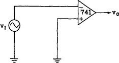
One way to view the operation of the circuit in Figure 3.2 is to consider it to be an open-loop amplifier. That is, with no feedback, the gain of the amplifier is simply the open-loop gain of the op amp itself. Since this gain value is very high (at least at low frequencies), we know the output will be driven to either +VSAT or −VSAT if the input is more than perhaps 1 microvolt or so above or below ground potential.
Since the output voltage is at one of the two saturation levels at all times (except during the short switching time), the circuit essentially converts the sinewave input into a square wave. The resulting square wave will have the same frequency as the input, but the amplitude will always swing between ±VSAT regardless of the value of the input voltage. Figure 3.3 illustrates the relationship between the input and output waveforms.
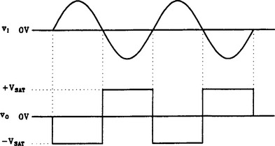
FIGURE 3.3 The input/output relationships for the zero-crossing detector shown in Figure 3.2
The output of a voltage comparator switches between two voltage limits (±VSAT in the case of the simple comparator in Figure 3.2). In a real op amp, it takes a small but definite amount of time for the output to switch between the two voltage levels. The maximum rate at which the output can change states is called the slew rate of the op amp and is specified in the manufacturer’s data sheet. If the input frequency is too high (i.e., changes too quickly), then the output of the op amp cannot change fast enough to keep up with the input. The initial effects of slew rate become evident by nonideal rise and fall times on the output waveshape. If the frequency continues to increase, the rise and fall times—which are established by the slew rate—become a significant part of the output waveform. Figure 3.4 illustrates the effects of slew rate on the output of the simple comparator circuit.

3.2.2 Numerical Analysis
For purposes of numerical analysis of the circuit shown in Figure 3.2, let us assume the following input signal characteristics:
| 1. Input frequency | 1.8 kilohertz |
| 2. Input voltage | 3 volts RMS |
| 3. Input reference | 0 volts |
Minimum Input Impedance.
The input impedance is established by the differential input resistance of the op amp. The input resistance of the 741 (RD) is listed in the manufacturer’s data sheet (Appendix 1) as at least 300 kilohms. The minimum input resistance, then, is computed as
It is important to note that without feedback the (−) input does not behave as a virtual ground.
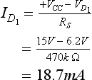
Maximum Input Current.
The maximum input current can be calculated by application of Ohm’s Law:

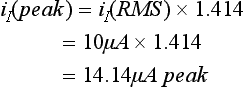
Since this is a sinusoidal waveform, we can convert it to a peak value if desired:
Output Voltage.
The limits of the output voltage in the circuit shown in Figure 3.2 are simply the values of ±VSAT. For ±15-volt power supplies and a load resistance of greater than 10 kilohms, the manufacturer’s data sheet in Appendix 1 lists a minimum output swing of ±12 volts. If we loaded the circuit with a resistance of less than 10 kilohms, we could expect the output levels to decrease.
3.2.3 Practical Design Techniques
For low-frequency noncritical applications, the simple circuit shown in Figure 3.2 can be very useful. For purposes of a design example, let us develop a circuit to satisfy the following requirements:
| 1. Input voltage | 500 millivolts peak |
| 2. Input frequency | 1 to 10 kilohertz |
| 3. Input reference | 0 volts |
| 4. Minimum output voltage | ±10 volts |
| 5. Load resistance | 68 kilohms |
Op Amp Selection.
We must select an op amp that can satisfy the output voltage requirements, survive the input voltage swings, and respond to the input frequencies. The manufacturer’s data sheet in Appendix 1 confirms that a 741 is capable of delivering a ±10-volt output. More specifically, the minimum output voltage with ±15-volt supplies and a load of greater than 10 kilohms is ±12 volts.
Additionally, the data sheet indicates that input voltage levels may be as high as the value of supply voltage. So far, the 741 seems like a good choice. Now let us consider the frequency effects.
The open-loop voltage comparator application requires the output voltage of the op amp to change from one extreme to the other. This change requires a finite amount of time. For DC or low-frequency applications, this amount of time is generally insignificant. As the input frequency increases, however, the switching time becomes a greater portion of the total time for one alternation of the input signal. In the extreme case, if the input alternation were shorter than the time required for the output to change states, then the comparator would cease to function properly. That is, the output voltage would not have time to reach its limits.
The slew rate of the op amp determines the maximum rate of change in the output voltage. The minimum acceptable rate of change is determined by the application. For purposes of example and as a good rule of thumb, let us design our circuit to have rise and fall times of no greater than 10 percent of the time for an alternation of the input signal. For our present design, the highest input frequency was specified as 10 kilohertz. The time for one alternation can be calculated from our basic electronics theory as
where t(period) = 1/frequency. In our case,
Our maximum rise and fall times will then be computed as
The minimum acceptable slew rate for our op amp can be computed with the following equation:
In our present example, the minimum acceptable slew rate is computed as
It is common to divide this result by 106 and express the slew rate in terms of volts per microsecond. In our case,
The slew rate for a 741 op amp is listed in the data sheet as 0.5 volts per microsecond. Clearly, this is too slow for our application. If we use the 741, our output signal will look more like a triangle wave than a square wave. Appendix 4 shows the data for another alternative.
The MC1741SC op amp should satisfy the voltage specifications of our design. Additionally, the minimum slew rate is listed as 10 volts per microsecond. We will use the MC1741SC for our design.
Figure 3.5 shows the resulting design. The oscilloscope displays in Figure 3.6 reveal the actual performance of the circuit.
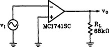

FIGURE 3.6 Oscilloscope displays showing the actual performance of the circuit in Figure 3.5. (Test equipment courtesy of Hewlett-Packard Company.)
3.3 ZERO-CROSSING DETECTOR WITH HYSTERESIS
Figure 3.7 shows the schematic diagram of a zero-crossing detector with hysteresis. At first glance, the configuration may resemble a basic amplifier circuit similar to those discussed in Chapter 2. A more careful examination, however, will reveal that the feedback is applied to the (+) input terminal. That is, the circuit is using positive feedback.
Resistors RF and R1 form a voltage divider for the output voltage. The portion of the output voltage that appears across R1 is felt on the (+) input of the op amp. This voltage establishes what is called the threshold voltage. When the output is positive, the voltage on the (+) input is called the positive, or upper, threshold voltage (VUT). The voltage on this same input when the output is negative is called the lower, or negative, threshold voltage (VLT). For the circuit in Figure 3.7, these two threshold levels will be the same magnitude but opposite polarity. In some circuits, it is desirable to have different values and/or different polarities for the upper and lower thresholds.
To examine the operation of the circuit, let us assume that the input voltage is at its most negative value and that the output is driven to its positive saturation level. A portion of the positive output voltage will be developed across R1 and appear on the (+) input. This is our upper threshold voltage. As long as the input voltage is below the value of the upper threshold voltage, the circuit will remain in its present condition (positive saturation).
Once the input voltage exceeds (i.e., becomes more positive than) the upper threshold voltage, the (−) pin becomes more positive than the (+) pin of the op amp. Basic op amp operation tells us that the amplifier will produce a negative output voltage. In our case, the output will drive all the way to its negative saturation limit.
Once the output reaches its negative limit, the (+) input has a different voltage—the negative, or lower, threshold voltage—on it. The circuit will remain in this stable condition as long as the input voltage is more positive than the lower threshold voltage.
Notice the voltages at which output switching occurs. When the input signal is rising, the switching point is determined by the upper threshold voltage. When the signal returns to a lower voltage, however, the output does not switch states as the upper threshold voltage is passed. Rather, the input voltage must go all the way down to below the lower threshold before the output will change states.
The difference between the two threshold voltages is called the hysteresis. The amount of hysteresis is determined by the values of the voltage divider consisting of RF and R1 and by the levels of output voltage (±VSAT in the present case).
Positive feedback makes the circuit more immune to noise. To understand this effect, consider the drawings in Figure 3.8, which represent a dual-ramp input voltage with superimposed noise pulses. The output voltage waveform (vO) for a circuit without hysteresis shows a response every time the combination of input voltage and noise crosses 0. For the circuit with hysteresis, however, once the output has changed states, the combination of input ramp and noise voltage must extend all the way to the opposite threshold voltage before the output will show a response.

3.3.2 Numerical Analysis
Let us now analyze the circuit shown in Figure 3.7. We shall determine the following values:
Upper Threshold Voltage.
The upper threshold voltage is the value of voltage that appears across R1 when the output is at its maximum positive level. In our present circuit, the maximum output is essentially +VSAT. We will use the lowest value given in Appendix 1 (10 volts) for +VSAT. The value of threshold voltage is computed by applying the basic voltage divider formula.
where VT is the total voltage across the series resistors R1 and RF. In our case, we have
This calculation reveals a significant limitation for this circuit. The value of threshold voltage is directly affected by the value of VSAT. That value, however, is far from constant. Appendix 1 indicates that VSAT can vary from a low value of 10 volts (with a heavy load) to as high as 14 volts when lightly loaded. The resulting variation in threshold voltage may be objectionable in some applications. If so, the feedback voltage can be regulated (e.g., by using a pair of zener diodes) for more consistent performance.
Lower Threshold Voltage.
The lower threshold voltage for the circuit shown in Figure 3.7 is computed using the same method, Equation (3.5), discussed for the upper threshold. The value is computed as

The lower threshold suffers from the same variations described for the upper threshold. Also notice that in this particular circuit, the upper and lower threshold voltages are equal in magnitude and positioned on either side of 0 volts. Other circuits may have dissimilar magnitudes for the two thresholds. Additionally, the thresholds are not necessarily centered around 0 in all detector circuits.
Hysteresis.
The hysteresis of the circuit shown in Figure 3.7 is simply the difference between the two threshold voltages. That is,
The higher the value of hysteresis, the more noise immunity offered by the circuit. In the present case, once the input voltage has crossed one of the threshold levels, it will take a noise pulse of the opposite polarity and with a magnitude of at least 1.82 volts before the output will respond.
In the case of equal ±VSAT voltages, the hysteresis may be computed directly with the following equation:
Maximum Frequency of Operation.
Since the output voltage of the zero-crossing detector switches between two extreme voltages, the upper frequency limit is more appropriately determined by considering the effects of slew rate rather than the falling amplification. You will recall that the slew rate of an op amp limits the rate of change of output voltage. For purposes of this calculation, we will determine the highest operating frequency that allows the output to switch fully between ±VSAT. If we exceed this frequency, the output amplitude will begin to diminish. The reduced output voltage will produce a similar reduction in threshold voltages and the hysteresis voltage.
Appendix 1 lists the slew rate of a 741 op amp as 0.5 volts per microsecond. The output must change from one saturation level to the other during the time for half of the input period (assuming a symmetrical output signal). For purposes of worst-case design, let us assume that the saturation voltages are at their highest magnitudes (listed as ±14 volts in Appendix 1). The minimum time required to switch between these two limits is computed as shown:
In the case of equal magnitudes of ±VSAT voltages, this can be expressed as
In our present case, the minimum switching time is determined as shown:
Since this corresponds to half of the period of the highest input frequency, we can determine the upper frequency as shown:
The above equation represents a worst-case situation. It should be noted, however, that the output waveform under these extreme conditions will more closely resemble a triangle waveform than a square wave. Whether or not this is objectionable is totally dependent upon the application. In cases where output rise and fall times must be short compared to the pulse width, the following equation can be used to determine the highest operating frequency for a particular ratio (ρ) of switching time (tS) to stable time (tP).
In the case of Figure 3.7, we have already computed tS as 56 microseconds. Now suppose we want the switching times (rise and fall) to be one-tenth (0.1) of the stable time (tP). This establishes our ratio ρ as 0.1. The highest frequency is then computed as
If the input waveform is such that the output will not be symmetrical, then tS establishes the shortest (either positive or negative) alternation of the output waveform. The highest frequency of operation, however, can be obtained when the output waveform is symmetrical.
3.3.3 Practical Design Techniques
Let us now design a zero-crossing detector circuit similar to that shown in Figure 3.7. We will design to achieve the following:
| 1. Upper threshold | +0.5 volts |
| 2. Lower threshold | −0.5 volts |
| 3. Hysteresis | 1.0 volts |
| 4. Highest operating frequency | 15 kilohertz |
| 5. Maximum ratio (ρ) of switching time to stable time | 0.2 |
| 6. Power supply voltages | ±15 volts |
Determine the Required Slew Rate.
In this type of application, slew rate is probably the most critical parameter with regard to op amp selection. The slew rate must be high enough to allow the output to switch between saturation levels within the allowed switching time (tS). The switching time is computed by using a transposed version of the f(max) equation. That is,
For the present circuits, we have
For purposes of op amp selection, we can assume that the output swings between the two power supply limits. That is, assume that ±VSAT - ±VCC. The required slew rate can then be computed as
Select an Op Amp.
Appendix 1 indicates that the slew rate for a 741 is only 0.5 volts per microsecond, which clearly eliminates this device as an option because we will require a slew rate of at least 5.4 volts per microsecond. Appendix 4, however, shows that the MC1741SC op amp has a minimum slew rate of 10 volts per microsecond. This will satisfy our present requirements nicely, and it is compatible with our power supply requirements. We will build our design around the MC1741SC op amp.
Determine RF and R1.
The ratio of RF and R1 is dependent on the ratio of VSAT voltage to hysteresis voltage. Appendix 4 indicates that the unloaded output swing will be approximately ±13 volts. We use this value for our computations. If the circuit is expected to drive a greater load (smaller load resistor), then the output will be correspondingly smaller. The ratio of RF to R1 is computed as follows:
More specifically, for the present circuit we have
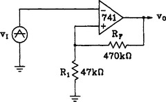
Many combinations of RF and R1 will produce a 25:1 ratio. We will select R1 and calculate the value of RF. If possible, we generally want both resistors in the range of 1.0 kilohm to 1.0 megohm, although these do not represent absolute limits. For purposes of this example, we select R1 to be 4.7 kilohms. Having done this, we can now compute RF by simply multiplying R1 by the RF/R1 ratio.
We will select a standard value of 120 kilohms.
This completes the design of the simple zero-crossing detector circuit. The schematic is shown in Figure 3.9. The circuit performance is shown by the oscilloscope displays in Figure 3.10. The original design goals are contrasted with the measured performance in Table 3.1.
TABLE 3.1
| Design Goal | Measured Values | |
| Upper threshold | +0.5 volts | +0.54 volts |
| Lower threshold | −0.5 volts | −0.51 volts |
| Hysteresis | 1.0 volts | 1.05 volts |
| Maximum switching ratio | 0.2 | 0.126 |

FIGURE 3.9 A zero-crossing detector designed for 1.0 volt hysteresis and operation up to 15 kilohertz.
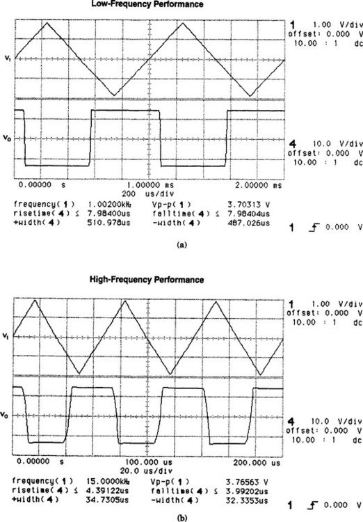
FIGURE 3.10 Waveforms showing the actual circuit performance of the zero-crossing detector shown in Figure 3.9.. (Test equipment courtesy of Hewlett-Packard Company)
3.4 VOLTAGE COMPARATOR WITH HYSTERESIS
Figure 3.11 is a schematic of an inverting voltage detector with hysteresis. The operation of this circuit is similar to that of the zero-crossing detector discussed in the last section, but the upper and lower thresholds are on either side of a reference voltage (VREF) rather than on either side of 0. The reference voltage can be either positive or negative. Note that if the reference is 0 volts, then the circuit is identical to the zero-crossing detector previously discussed.
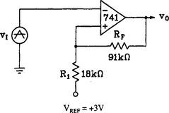
To begin the discussion, let us assume that the input voltage is at its most negative value and that the output of the op amp is driven to its +VSAT level. The +VSAT output is divided between RF and R1 in normal voltage divider fashion. The voltage appearing across R1 plus the value of the reference voltage determines the voltage on the (+) input terminal. This is the upper threshold voltage. The circuit will remain in this condition as long as the input voltage is below the voltage on the (+) terminal.
Now suppose that the input voltage is allowed to exceed the upper threshold voltage that is present on the (+) input. If this happens, the output will quickly go to the −VSAT level. RF and R1 will divide the negative output voltage. The portion across R1 plus the value of the reference voltage determines the voltage on the (+) input terminal. This is the lower threshold voltage. The circuit will remain in this stable condition until the input voltage falls below the negative threshold voltage.
In many practical comparator circuits, the reference voltage is provided by a zener diode (see, for example, Figure 3.12 further on) or other voltage regulator circuit.

3.4.2 Numerical Analysis
We will now analyze the circuit shown in Figure 3.11 to determine the following:
Upper Threshold Voltage.
The upper threshold voltage is the value of the voltage that appears across R1 when the output is at its maximum positive level, plus the value of the reference voltage. Appendix 1 lists a minimum value of 10 volts for +VSAT. The value of the threshold voltage is computed by applying the basic voltage divider formula to RF and R1 and then adding the result to the reference voltage (VREF).
For this particular circuit, we have
As with the zero-crossing detector previously discussed, the threshold voltages vary with VSAT. If this variation is objectionable, then the output can be regulated by zeners, as discussed in Section 3.6.
Lower Threshold Voltage.
The lower threshold voltage for the circuit shown in Figure 3.11 is computed using the same method discussed for the upper threshold:
The lower threshold suffers from the same variations described for the upper threshold. Also, notice that in this particular circuit, the upper and lower threshold voltages are both above 0 volts but equally spaced on either side of the reference voltage. The thresholds in some circuits are not equally spaced around the reference.
Hysteresis.
The hysteresis of the circuit shown in Figure 3.11 is simply the difference, as given by Equation (3.6), between the two threshold voltages. That is,
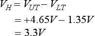
Recall that the value of hysteresis primarily determines the noise immunity offered by the circuit. In the present case, once the input voltage has crossed one of the threshold levels, it will take a noise pulse of the opposite polarity and with a magnitude of at least 3.3 volts before the output will respond.
The hysteresis in this circuit may also be computed directly with Equation (3.7).
Maximum Frequency of Operation.
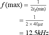
The upper frequency of operation is limited in the same manner as the zero-crossing detector discussed previously. This frequency is estimated with Equation (3.10):
where ts is computed with Equation (3.8) as shown:
Or, in the usual case of symmetrical power supplies, we can simply use Equation (3.9) as follows:
In our present case, let us determine the minimum switching time with Equation (3.9):

Substituting this value into the maximum frequency formula, Equation (3.10), gives us
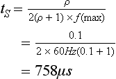
The above equation represents a worst-case situation for a symmetrical output waveform. As noted in the zero-crossing circuit, the output waveform under these extreme conditions will more closely resemble a triangle waveform than a square wave. In cases where output rise and fall times must be short compared to the pulse width, Equation (3.11) can be used to determine the highest operating frequency for a particular ratio (ρ) of switching time (tS) to stable time (tP). In the case of Figure 3.11, we have already computed tS as 40 microseconds. Now suppose we want the switching times (rise and fall) to be one-eighth (0.125) of the stable time (tP). This establishes our ratio ρ as 0.125. The highest frequency is then computed with Equation (3.11) as
3.4.3 Practical Design Techniques
Now let us design a voltage comparator circuit with hysteresis and obtain the following performance:
| 1. Upper threshold | −4.25 volts |
| 2. Lower threshold | −7.75 volts |
| 3. Hysteresis | 3.5 volts |
| 4. Highest operating frequency | 60 hertz |
| 5. Maximum ratio (ρ) of switching time to stable time | 0.1 |
| 6. Power supply voltages | ±15 volts |
Determine the Required Slew Rate.
The slew rate must be high enough to allow the output to switch between saturation levels within the allowed switching time (tS). The switching time is computed with Equation (3.12) as follows:
For purposes of op amp selection, we can assume that the output swings between the two power supply limits. That is, assume that ±VSAT = ±VCC. The required slew rate can then be computed with Equation (3.13) as

These calculations assume a 50-percent duty cycle on the output waveform. If the output is asymmetrical, then the shortest allowable alternation is given as
Select an Op Amp.
Appendix 1 indicates that the slew rate for a 741 is 0.5 volts per microsecond, which exceeds our requirement of at least 0.04 volts per microsecond. The power supply requirements are also compatible with our stated design requirements. We will build our design around the 741 op amp.
Determine RF and R1.
The ratio of RF and R1 is dependent on the ratio of VSAT voltage to hysteresis voltage. Appendix 1 indicates that the lightly loaded (RL > 10 kΩ) output swing will be typically ±14 volts. We will use this value for our computations. If the circuit is expected to drive a greater load (smaller load resistor and/or feedback network), then the output will be correspondingly smaller. The ratio of RF to R1 is computed with Equation (3.14).
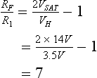
We select R1 and calculate the value of RF. For purposes of this example, we select R1 to be 33 kilohms. Having done this, we can now compute RF by applying Equation (3.15) where the ratio (RF/R1) is known.
Calculate VREF.
A simple way to calculate the required value of VREF is to apply Equation (3.18).
where VLT and VH are the lower threshold and hysteresis voltages, respectively. In our present case, we can determine VREF as shown:
For purposes of illustration, let us derive this reference voltage from a zener diode network across the −15-volt supply. As long as the equivalent (Thevenin) resistance of the zener circuit is small compared to RF and R1 (the usual case), it will not affect our previous selection of components.
Appendix 5 shows the data sheet for a family of zener diodes. One of the listed devices is the 1N5233B, which is a 6.0-volt, 1/2-watt zener diode. The maximum zener current can be estimated by applying the power formula:
where PZ and VZ are the power and voltage ratings of the zener. In the case of the 1N5233B, the maximum current is
This establishes the upper limit of zener current, and even this must be derated for temperatures above 25°C. The zener test current (IZT) is listed as 20 milliamps, which is generally a good quiescent current choice.
The series current limiting resistor for the zener regulator can be computed as follows:
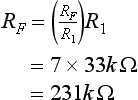
Finally, we will choose the standard value of 470 ohms, which completes our design. The final schematic is shown in Figure 3.12. The waveforms in Figure 3.13 reveal the performance of the circuit. The original design goals are contrasted with the measured performance in Table 3.2.
TABLE 3.2
| Design Goal | Measured Value | |
| Upper threshold | −4.25 volts | −4.25 volts |
| Lower threshold | −7.75 volts | −7.813 volts |
| Hysteresis | 3.5 volts | 3.56 volts |
| Maximum switching ratio | 0.02 | 0.012 |
FIGURE 3.13 Waveforms showing the performance of the circuit shown in Figure 3.12. (Test equipment courtesy of Hewlett-Packard Company.)
3.5 WINDOW VOLTAGE COMPARATOR
A basic op amp window detector circuit, shown in Figure 3.14, is essentially a dual comparator circuit and produces a two-state output that indicates whether or not the input voltage (vI) is between the limits (i.e., within the window) established by the ±VREF voltages. It is frequently used to sound an alarm or signal a control circuit when a measured variable (vI) goes outside of a preset range. The reference voltages in Figure 3.14 are established by two zener diode circuits.
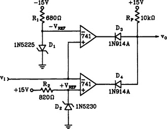
FIGURE 3.14 A window detector is used to determine whether the input voltage (vI) is within the limits of ±VREF.
To examine the operation of the circuit, let us start by assuming that the input voltage is within the window. That is, the input voltage is less than +VREF and greater than −VREF. Under these conditions, the outputs of both op amps will be driven to the +VSAT level. This reverse-biases the two isolation diodes (D3 and D4) and allows the output (vO) to rise to +15 volts, indicating an “in window” condition. (Note that if the positive saturation levels of the op amps are sufficiently low, the isolation diodes will not be reverse-biased but the output will still be at its most positive level.)
Now suppose that the input either exceeds +VREF or falls below −VREF. In either of these cases, the output of one of the two op amps will go to the −VSAT level and forward-bias its associated isolation diode. This will cause the output of the circuit (vO) to be pulled to −15 volts (ideally). In practice, the output voltage will be equal to the negative saturation level plus the forward voltage drop of the conducting isolation diode. This negative level indicates an “out of window” condition.
3.5.2 Numerical Analysis
Let us now analyze the behavior of the circuit shown in Figure 3.14 in greater detail. We shall determine the following characteristics:
+VREF.
The value of +VREF is established by the 1N5230 zener diode. Appendix 5 indicates that this is a 4.7-volt zener, so +VREF is approximately +4.7 volts. If desired, we can determine the amount of zener current with Equation (3.20) (transposed):

VREF.
The 1N5225 zener diode is used to establish the −VREF source. Appendix 5 lists the 1N5225 as a 3.0-volt zener. Its current can be calculated with Equation (3.20) (transposed) as

Output Voltage (vO).
The upper limit of vO occurs when both of the isolation diodes are reverse-biased or effectively open. This means that the pull-up resistor (RP) has essentially no current flow and therefore no voltage drop across it. Since RP drops no voltage under these conditions, the output will be at a +15-volt level. As mentioned previously, if +VSAT is sufficiently low, the isolation diode will not be reverse-biased and the output voltage (vO) will be less than +15 volts (+VSAT + VF, where VF is the forward voltage drop of the diode).
If either of the op amp outputs is forced to its −VSAT level, then the associated isolation diode will be forward-biased. Appendix 1 indicates that the −VSAT will be about −11 volts. The current through RP can now be estimated as follows:
where VF is the forward voltage drop of the isolation diode (typically 0.7 volts). In our present case, we can compute IRP as
The actual output voltage (vO) under these conditions is determined as follows:
This same result can be obtained by applying Kirchhoff’s Voltage Law—that is,
3.5.3 Practical Design Techniques
Let us now design a window detector to meet the following specifications:
| 1. Upper window limit | +10 volts |
| 2. Lower window limit | +7.5 volts |
| 3. Power supply | ±15 volts |
| 4. Input frequency | 0 to 100 Hz |
Select the Op Amp.
Since the circuit is being driven by a very low-frequency source, the high-frequency characteristics of the op amp are unimportant to us. The DC stability of the op amp is more important in circuits like this and will be determined by the requirements of the application being considered. If the switching speed of the device is important for an application that has a higher input frequency, then you would do well to select an op amp that is specifically designed for fast comparator applications.
Select the Zener Diodes.
Appendix 5 lists a family of zener diodes. The 1N5236 and 1N5240 devices will satisfy the requirements for our lower and upper reference voltages of 7.5 volts and 10 volts, respectively.
Calculate the Zener-Current Limiting Resistors.
Unless we have some reason to do otherwise (e.g., ultra-low current designs), we can use the zener test current as the design value. Appendix 5 lists 20 milliamps as the test current for both diodes. Basic circuit theory, as given in Equation (3.20), allows us to compute the values of current limiting resistors.
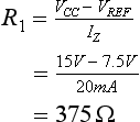
We will choose a standard value of 390 ohms. In a similar manner,

We choose the next higher standard value of 270 ohms. Note that in this particular case, both zeners will be connected across the positive supply voltage because we require both references to be positive.
Select RP.
The correct value of RP is determined by two primary considerations:
Since we have no information regarding the driven circuit, let us select RP such that the op amp output current is limited to 5 milliamps. This calculation, from Equation (3.21), is based on Ohm’s Law as follows:
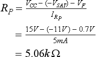
Let us select the next higher standard value of 5.1 kilohms.
Select the Isolation Diodes.
The requirements for the isolation diodes are not stringent. The two primary parameters that need to be considered are
The maximum current is the same as the value of the op amp output current. In our case, we have designed this to be 5 milliamps. The maximum reverse voltage (ignoring diode drops) is approximately equal to the difference between +VSAT of one op amp and −VSAT of the other. That is,
Appendix 6 shows the characteristics for a 1N914A diode. Almost any diode will satisfy our modest requirements. The 1N914A is a standard, low-cost diode that we can use for this application.
This completes the design of the window detector circuit. The final schematic is shown in Figure 3.15. Figure 3.16 shows the actual waveforms produced by the circuit. Table 3.3 compares the original design goals with the measured circuit performance.
TABLE 3.3
| Design Goal | Measured Value | |
| Upper window limit | +10 volts | +10 volts |
| Lower window limit | +7.5 volts | +7.5 volts |

FIGURE 3.15 A window detector designed for a lower limit of +7.5 volts and an upper limit of +10 volts

FIGURE 3.16 Oscilloscope displays showing the performance of the circuit in Figure 3.15. (Test equipment courtesy of Hewlett-Packard Company.)
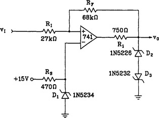
3.6 VOLTAGE COMPARATOR WITH OUTPUT LIMITING
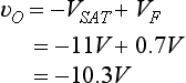
The voltage comparator shown in Figure 3.17 is configured to be noninverting. Additionally, the output uses two zener diodes (D2 and D3) to limit the swing of vO. The zener pair, along with resistor R1, acts like a bidirectional, biased limiter circuit. D1 and current limiting resistor RS establish the reference voltage. Feedback resistor RF, in conjunction with RI, establishes hysteresis for the circuit.
For purposes of discussion, let us assume that the input is well below the upper threshold voltage. Since this is a noninverting circuit, we know that the output of the op amp will be driven to the −VSAT level. The zener pair in the output circuit, along with R1, regulates the −VSAT voltage to a value established by D3. This reduced and regulated voltage appears as vO.
Resistors RF and RI form a voltage divider that appears between the regulated vO and the changing input voltage. The circuit will remain in this stable condition as long as the (+) input of the op amp remains lower than the reference voltage on the (−) input.
As the input voltage increases, the voltage on the (+) input also increases. Once the (+) input goes above the voltage on the (−) input, even momentarily, the output of the op amp will go toward the +VSAT level. This rising potential, through RF, further increases the potential on the (+) input pin. With the output of the op amp at the +VSAT level, diode D2 establishes the value of voltage at vO. Again, the circuit will remain in this state until the voltage on the (+) input falls below the voltage on the (−) terminal. Note that because the rising output has increased the potential on the (+) input, the actual input voltage (vI) will have to go to a much lower level to cause the circuit to switch states. This effect is, of course, the very nature of hysteresis.
If the input voltage now decreases to a level that causes the voltage on the (+) pin to fall below the voltage on the (−) pin, then the circuit will switch back to its original state.
3.6.2 Numerical Analysis
Now let us extend our analysis of Figure 3.17 to calculate the following:
Upper Threshold Voltage.
The upper threshold voltage can be found by applying Kirchhoff’s Law and basic circuit theory to the resistor network RI and RF. Our knowledge of op amp operation tells us that no substantial current enters or leaves the (+) pin. Therefore, i1 = i2 in Figure 3.18. At the instant vI reaches the upper threshold, the junction of RF and RI will just equal VREF. This is so labeled on Figure 3.18.

FIGURE 3.18 Basic circuit theory can be used to compute the upper threshold voltage of the circuit in Figure 3.17.
Using Ohm’s Law, we can write expressions for the values of i1 and i2:

If we equate these two currents, we get
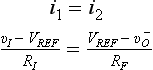
Some algebraic manipulation gives us the expression for vI at the moment it reaches the upper threshold:
In the present example, vO− equals the voltage of D3 (−5.6 volts as listed in Appendix 5) during this period of time. The reference voltage is 6.2 volts (see Appendix 5). Substituting values enables us to calculate the value of the upper threshold voltage:
This value can be made slightly more accurate by including the effects of the forward voltage drop of D2 (about 0.7 volts). That is, vO− will equal the voltage of D3 plus the forward voltage drop of D2, or −6.3 volts. If this effect is included, the threshold is computed to be 11.2 volts.
Lower Threshold Voltage.
A similar application of basic circuit theory when the output is at the +VSAT level and the input is approaching the lower threshold voltage yields the following expression for the lower threshold voltage:
Recognizing that vO+ will be equal to the voltage of D2 (3.3 volts) during this time, we can calculate the value of lower threshold voltage:
If the forward voltage drop of D3 is included in the calculation, the threshold voltage will be computed as 7.07 volts.
Hysteresis.
Hysteresis is simply the difference between the two threshold voltages. In our present case, hysteresis is computed as shown in Equation (3.6):

If the diode drops are included, the hysteresis will be computed as 4.13 volts.
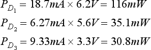
Zener Currents.
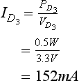
The current through D1 can be computed from Equation (3.20) as follows:
The reverse current through D3 is computed with the following expression:
Continuing with the calculations, we get
Note that the minus sign simply indicates direction and is of no significance to us at this time. D2 current is computed in a similar manner as shown:
Substituting values for the present circuit gives us
The power dissipation of the zeners can be found by applying the basic power equation P = IV, where I and V are the current and voltages associated with a particular zener. In our particular case,
3.6.3 Practical Design Techniques
We will now design a voltage comparator with output limiting that satisfies the following specifications:
| 1. Upper output voltage (vO+) | +5.0 volts |
| 2. Lower output voltage (vO− | −4.0 volts |
| 3. Upper threshold voltage | +2.0 volts |
| 4. Lower threshold voltage | +0.8 volts |
| 5. Power supply | ±15 volts |
| 6. Op amp | 741 |
These specifications (i.e., input and output requirements) would normally be dictated by the application.
Compute Hysteresis Voltage.
Our first step will be to calculate the required hysteresis voltage. This is, very simply, the difference between the two threshold voltages from Equation (3.6).

Compute RF and RI.
The ratio of RF to RI is determined by the ratio of the output voltage swing to the hysteresis voltage. That is,
In our design example, the required RF/RI ratio is computed as shown:
We will now select RI and compute RF. We will choose 10 kilohms for resistor RI. The feedback resistor RF can now be computed, from Equation (3.15), as shown:
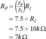
The factor 7.5 in the above equation is simply the RF/RI ratio previously computed.
Select the Output Zener Diodes.
The voltage rating of the two zener diodes is determined by the stated output voltage swing. That is,
Similarly, the voltage rating for D3 is computed as
Values for the present circuit are
The power ratings for the zeners are not critical, but must be noted for subsequent calculations. By referring to Appendix 5, we can select a 1N5229 and a 1N5226 for diodes D2 and D3, respectively. We also observe that both of these diodes are rated at 500 milliwatts.
Compute R1.
Resistor R1 is a current limiting resistor for the zener diodes. First, we will compute the maximum allowable currents through each of the zeners, using Equation (3.19).

Since both of these exceed the short-circuit output current of the 741, we will have to limit the current well below the maximum amount. Let us plan to limit it to 5 milliamps.
Next we compute the minimum values for R1 in order to limit the diode currents to the desired value by applying Ohm’s Law. The minimum value as dictated by D2 is found, from Equation (3.20), to be
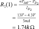
Similarly, the value required to limit the current through D3 is computed as
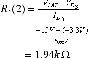
The larger of these two values (1.94 kilohms) sets the lower limit on R1. We will select the next higher standard value of 2 kilohms for R1.
Select the Reference Zener Diode.
The required reference voltage can be determined by using the following equation:
In our present design, the required reference is calculated as follows:
A brief scan of Appendix 5 reveals that it may be very difficult to locate a 1.3-volt zener. Let us rely on our knowledge of basic semiconductors to discover an alternative. Recall that a forward-biased silicon diode has about 0.6 to 0.7 volts and remains fairly constant. We can obtain the equivalent of a 1.3-volt zener by using two series silicon diodes. Appendix 6 lists the data for 1N914A diodes. A 1N914A diode will have about 0.64 volts across it with a forward current of 0.25 milliamps. Similarly, this same diode will have about 0.74 volts across it with a forward current of 1.5 milliamps. Let us select 1N914A diodes for our application and establish a forward current of about 0.5 milliamps.
Determine the Value of RS.
The purpose of resistor RS is to limit the current through reference diode D1. In our case, it will limit the current through two series 1N914A diodes. The value of RS is computed, from Equation (3.20), as follows:
where IREF is the specified current through the reference diode. For our design, RS is calculated as shown:
We will choose the standard value of 27 kilohms for RS.
This completes the design of our voltage comparator with output limiting. The final schematic is shown in Figure 3.19, and the actual performance of the circuit is shown in Figure 3.20 by means of oscilloscope displays. The design goals are contrasted with the measured circuit values in Table 3.4.
TABLE 3.4
| Design Goal | Measured Value | |
| Output voltage (+) | +5.0 volts | +5.0 volts |
| Output voltage (−) | −4.0 volts | −4.06 volts |
| Upper threshold voltage | +2.0 volts | +2.0 volts |
| Lower threshold voltage | +0.8 volts | +0.77 volts |
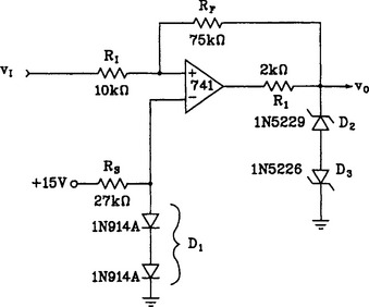
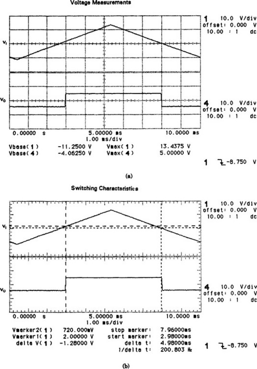
FIGURE 3.20 Oscilloscope displays showing the behavior of the comparator in Figure 3.19. (Test equipment courtesy of Hewlett-Packard Company.)
3.7 TROUBLESHOOTING TIPS FOR VOLTAGE COMPARATORS
Comparator circuits are generally some of the easier op amp circuits to trouble shoot, provided you pay close attention to the symptoms and keep the basic theory of operation in mind at all times. If the circuit worked properly at one time (i.e., it does not have design flaws), then the symptoms of the malfunction will normally fall into one of the following categories:
Output Saturated.
It is always a good first check to verify the power supply voltages. A missing supply can cause the output to go to the opposite extreme.
If the power supplies are both correct, then compare the voltage readings on the (+) and (−) inputs of the op amp. If the polarity on the two inputs periodically switches (i.e., one input becomes more positive than the other and then later changes so that it is less positive than the other), then the op amp is a likely suspect. That is, the inputs directly on the op amp are telling the device to switch and the op amp has the correct power source, yet the output remains in saturation. The op amp is the most probable trouble.
If, on the other hand, the (+) and (−) input terminal measurements reveal that one of the inputs is always more positive than the other, then the op amp is not being told to change states. In this case, you should check the input signal for proper voltage levels. Pay particular attention to any DC offset signals that may be present. A DC offset at the input can shift the entire operation so far off center that the input signal cannot cause the op amp to switch.
If the input signal is correct, verify the proper voltage on the reference input. If this is incorrect, the problem lies in the reference circuit (i.e., voltage divider, zener diode, etc.).
If both the input signal and the reference voltages are correct but one of the input pins continues to be more positive than the other at all times, measure the output of the op amp (particularly in circuits with output limiting). Although the output is at an extreme voltage, determine if the extreme voltage is one of the expected levels (e.g., a proper zener voltage) or some higher voltage. If the level is incorrect (i.e., too high), then suspect one of the zener diodes in the output.
Incorrect Switching Levels.
Although there are many things that can cause minor shifts in switching levels (e.g., component value drifts), some are more probable than others. If the circuit has adjustable components, such as a variable reference voltage, suspect this first. If the variable components are properly adjusted but the problem remains, suspect any solid-state components other than the op amp (e.g., zener diodes).
The zeners can be checked for proper operation by measuring the voltage across them. A forward-biased zener will drop about 0.7 volts; a reverse-biased zener should have a voltage drop that is approximately equal to its rated voltage. Keep in mind that zeners are not precision devices. For example, a 5.6-volt zener that drops 6 volts is probably not defective.
As a last resort, verify the resistance values. Resistor tolerances in a low-power circuit of this type do not present problems very often.
3.8 NONIDEAL CONSIDERATIONS
For many comparator applications, slew rate is the primary nonideal parameter that must be considered. This limitation was discussed in earlier sections, along with methods for determining the effects of a finite slew rate. Additionally, the zener diodes become less ideal as the input frequency is increased.
Throughout the earlier sections of this chapter, it was assumed that the op amp changed states whenever the differential input voltage passed through 0. The input bias current for the op amp, however, can cause the actual switch point to be slightly above or below 0. This problem is minimized by keeping the resistance between the (−) input to ground equal to the resistance between the (+) input and ground.
Input offset voltage is another nonideal op amp parameter that can affect the switching points of the comparator. The effect of a non-0 input offset voltage can be canceled by utilizing the offset null terminals (discussed in Chapter 10). Appendix 4 illustrates the proper way to utilize the null terminals on an MC1741SC op amp. Note, however, that different op amps use different techniques for nulling the effects of input offset voltage. Therefore, you must refer to the manufacturer’s data sheet for each particular op amp.
The errors caused by the input bias currents and the input offset voltage can be totally eliminated by utilizing the nulling terminals. Unfortunately, however, the required level of compensation varies with temperature. Thus, although you may completely cancel the nonideal effects at one temperature, the effects will likely return at a different temperature. For many, if not most, comparator applications, this latter drift does not present severe problems. If the application demands greater stability, an op amp that offers optimum performance in these areas should be initially selected.
REVIEW QUESTIONS
1. Refer to Figure 3.7. Which component(s) is (are) used to determine the threshold voltages?
2. Refer to Figure 3.9. If resistor R1 develops a short circuit, describe the effect on circuit operation. Will there still be a rectangular wave on the output pin?
3. Refer to Figure 3.9. If resistor RF is reduced in value, describe the relative effect on the circuit hysteresis.
4. Refer to Figure 3.7. If resistor R1 is changed to 68 kilohms, what is the value for the upper threshold voltage? Does this resistor change affect the circuit hysteresis (VSAT = 10V)?
5. Refer to Figure 3.14. If resistor R1 is reduced in value (and no components are damaged), what is the effect on the negative threshold (assume ideal zeners)?
6. Refer to Figure 3.14. If diode D3 becomes open, describe the effect on circuit operation.
7. Refer to Figure 3.15. Describe the effect on circuit operation if diode D1 develops a short circuit.
8. Refer to Figure 3.17. What is the purpose of RS? Will the circuit still appear to operate correctly if RS is reduced to one-half its original value as long as no components are damaged? Explain.
9. Sketch a simple graph of voltage versus time that illustrates the relationship between the voltages at the following points in Figure 3.17: vI, vO, and the output pin of the op amp. Be sure to indicate relative voltage amplitudes and phase relationships.
10. Refer to Figure 3.19. What is the effect on circuit operation if RS is returned to a +20-volt supply instead of the +15-volt source shown in the figure?