Active Filters
5.1 FILTER FUNDAMENTALS
A filter, be it an oil filter, a lint filter, a furnace filter, or an active filter, accepts a wide spectrum of inputs, but only passes certain of these inputs through to the output. In some cases, it may pass through the “good stuff” while it catches the “bad stuff.” An oil filter in your car is one example. Other applications require a filter to catch the “good stuff” and let the “bad stuff” pass through. A gold prospector’s sieve is an example of this type of filter action. In both of the preceding examples, the filter discriminates between “good“ and “bad” on the basis of physical size (i.e., size of the dirt particle). In the filters discussed in this chapter, the “good” and “bad” signals will be classified on the basis of their frequency. The input will be a broad range of signal frequencies. The filter will allow a certain range of them to pass and will reject others.
Electronic filters designed to discriminate as a function of frequency can be broadly grouped into five classes:
| 1. Low pass | Allows frequencies below a specified frequency to pass through the filter circuit. |
| 2. High pass | Allows frequencies above a specified frequency to pass through the filter circuit. |
| 3. Bandpass | Allows a range or band of frequencies to pass through the filter circuit while rejecting frequencies higher or lower than the desired band. |
| 4. Band reject | Rejects all frequencies within a certain band, but passes frequencies higher or lower than the specified band. Also called a band-stop filter. |
| 5. Notch | Essentially a band-stop filter with a very narrow range of frequencies that are rejected. |
Figure 5.1 shows the general frequency response curves for each of the basic filter types. The exact nature of a given curve will vary with the type of circuit implementation. Most notably, the slope of the curve between the “pass” and “reject” regions of the filter varies greatly with different filter designs.

There are seemingly endless ways to achieve the various filter functions listed. Each method of implementation has its individual advantages and disadvantages for a particular application. In this chapter, we will select a representative filter design for each basic filter type. In each case, we will discuss its operation, numerically evaluate its performance, and, finally, design one to satisfy a given design goal. Band reject and notch filters will be treated as one general class.
An important consideration regarding active filters is how sharply the frequency response drops off for frequencies outside of the passband of the filter. In general, the steeper the slope of the curve, the more ideal the filter behavior. If the slope becomes too steep, however, the filter becomes unstable and is prone to oscillations. It is common to express the steepness of the slope in terms of dB per decade where a decade represents a factor of 10 increase or decrease in frequency. For example, suppose a low-pass filter had a 20-dB-per-decade slope beyond the cutoff frequency. This means that if the input frequency is increased by a factor of 10, then the output will decrease by 20 dB. If the input frequency is again increased by a factor of 10, then the output will decrease another 20 dB, or 40 dB from the first measurement. Typical filter circuits have slopes ranging from 6 to 60 dB per decade or more.
In the case of bandpass, bandstop, and notch filters, we often describe the steepness of the slopes in another way. The ratio of the center frequency (fC) to the bandwidth (bw) gives us an indication of the sharpness of the cutoff region. The ratio fC/bw is called the Q of the circuit. The higher the Q, the sharper the cutoff slopes of the filter.
The term Q is also used with reference to low-pass and high-pass filters, but it must be interpreted differently. The output of some filters peaks just before the edge of the passband. The Q of the filter indicates the degree of peaking. A Q of 1 has only a slight peaking effect. A Q of less than 1 reduces this peaking, while a Q greater than 1 causes a more pronounced peaking. There is usually a trade-off between peaking (generally undesired) and steepness (generally desired) of the slope. The high- and low-pass filter designs in this chapter use a Q of 0.707, which produces a very flat response.
5.2 LOW-PASS FILTER
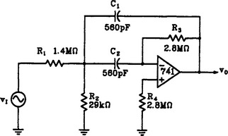
Figure 5.2 shows one of the most common implementations of the low-pass filter circuit. This particular configuration is called a Butterworth filter and is characterized by a very flat response in the passband portion of its response curve.

Ideally, a low-pass filter will pass frequencies from DC up through a specified frequency, called the cutoff frequency, with no attenuation or loss. Beyond the cutoff frequency, the filter ideally offers infinite attenuation to the signal. In practice, however, the transition from passband to stopband is a gradual one. The cutoff frequency is defined as the frequency that passes with a 70.7-percent response. This, of course, is the familiar half-power point referenced in basic electronics theory.
5.2.1 Operation
Let us try to understand the operation of the low-pass filter circuit shown in Figure 5.2 from an intuitive or logical standpoint before evaluating it numerically. First, mentally open-circuit the capacitors. This modified circuit is shown in Figure 5.3, which is essentially how the circuit will look at low frequencies when the capacitive reactance of the capacitors is high. We can see that this amplifier is connected as a simple voltage follower circuit. Resistor R3 is included in the feedback loop to compensate for the effects of bias currents flowing through R1 and R2. For low frequencies, then, we expect to have a voltage gain of about unity.

FIGURE 5.3 A low-frequency equivalent circuit for the low-pass filter shown in Figure 5.2.
Now let us mentally short-circuit the capacitors in Figure 5.2 to get an idea of how the circuit looks to high frequencies where the capacitive reactance is quite low. This equivalent circuit is shown in Figure 5.4.
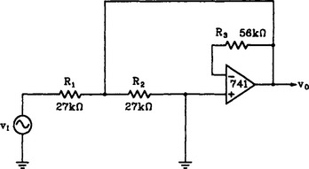
FIGURE 5.4 A high-frequency equivalent circuit for the low-pass filter shown in Figure 5.2.
First, notice that the (+) input of the amplifier is essentially grounded. This should eliminate any chance of signals passing beyond this point. The junction of R1 and R2 is effectively connected to the output of the op amp. This, you will recall, is a very low impedance point, so for high frequencies, the junction of R1 and R2 also has a low impedance to ground.
As our preliminary analysis indicates, the low frequencies should receive a voltage gain of about 1, and the high frequencies should be severely attenuated. We are now ready to confirm this numerically.
5.2.2 Numerical Analysis
The three primary considerations in active filters are
Cutoff Frequency.
In the case of the circuit in Figure 5.2, the cutoff frequency is the frequency that causes the output amplitude to be 70.7 percent of the input. We can compute this frequency with Equation (5.1),
where R = R1 = R2. For the circuit in Figure 5.2, the cutoff frequency is computed as follows:
Filter Q.
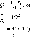
The Q of the circuit in Figure 5.2 is computed with Equation (5.2).
The value of 0.707 produces a maximally flat curve in the passband. That is, the response curve has minimal peaking at the edge of the passband. This is a common choice for Q.
Input Impedance.
The input impedance is an important consideration because it determines the amount of loading presented by the filter to the circuit driving the filter. The exact value of input impedance will vary dramatically with frequency. At very low frequencies, the input impedance approaches that of the standard voltage follower amplifier. As the input frequency increases, the input impedance decreases. The ultimate limit for the dropping input impedance is the value of R1. Expressing this as an equation gives us
In the case of the circuit in Figure 5.2, we can be assured that the input impedance will never be lower than 27 kilohms.
5.2.3 Practical Design Techniques
Let’s now design a low-pass filter similar to the circuit in Figure 5.2. The design goal for our filter is
| 1. Cutoff frequency | 1.5 kilohertz |
| 2. Q | 0.707 |
| 3. Input impedance | >10 kilohms |
Compute the Ratio of C2/C1.
From Equation (5.2), we can see that the ratio of C2/C1 determines the Q of the circuit. Therefore, since we know Q (from the design criteria), we can compute the capacitor ratio by transposing Equation (5.2).

This tells us that C2 will have to be twice as large as C1. In general, the value of C2 is determined with Equation (5.4).
We can now select C1 to be any convenient value and then double it to get C2. For this design, let us choose C1 as a 3300-picofarad capacitor. We can then make C2 a 6600-picofarad ideally, or perhaps a 6800-picofarad as this is a standard size.
Compute R1 and R2.
R1 and R2 should be within the general range of 1.0 to 220 kilohms. And, of course, R1 must be larger than the minimum required input impedance (10 kilohms in this case). If the following calculation produces a value for R1 and R2 that does not comply with these restrictions, then a different value must be selected for C and the resistor values recalculated. We compute the resistance value by applying Equation (5.1).

Determine the Value of R3.
The value for resistor R3 is calculated in the same way as for a simple voltage follower. That is, we want equal DC resistances between each op amp input and ground. For the circuit in Figure 5.2, we can compute R3 with Equation (5.5).
Substituting values for our present circuit gives us
We will select the nearest standard value of 47 kilohms for R3.
Select the Op Amp.
There are three op amp parameters that we should evaluate before specifying a particular op amp for our low-pass filter:
Since our op amp is operated as a voltage follower, the required bandwidth of the amplifier is essentially the same as the cutoff frequency. That is,
In the case of our present circuit, our op amp must have a bandwidth of greater than 1.5 kilohertz. In many cases, including this one, the bandwidth will not be a limiting factor because the op amp is operated at unity gain.
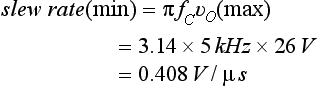
The minimum required slew rate for the op amp can be estimated with Equation (5.7),
where fC is the filter cutoff frequency and vO is the highest expected peak-to-peak output swing. If the application clearly has externally imposed limits on the maximum output amplitude, then use them. If the maximum output amplitude is not specifically known, as in the present case, then design for worst case and assume that the signal will swing between the ±VSAT levels. In the present circuit, the required op amp slew rate (using ±13 volts as the saturation limits) is computed as
Finally, the minimum op amp corner frequency may be estimated with Equation (5.8),
where AOL is the low-frequency, open-loop gain of the op amp and fC is the filter cutoff frequency. The corner frequency of the op amp is the one where the open-loop gain has dropped to 70.7 percent of its low-frequency or DC value. If we choose a 741 (AOL = 50,000), it must have a corner frequency greater than
Let us consider a 741 op amp for this application. Appendix 1 lists the data for the 741. The minimum bandwidth and slew rate requirements for our application are exceeded by the 741’s ratings. By referring to the graph of open-loop frequency response in Appendix 1, we can estimate the corner frequency of the 741 as about 5 hertz. Again, this exceeds our requirements, so let us choose a 741 for our design.
The schematic diagram of our completed low-pass filter design is shown in Figure 5.5. This circuit configuration provides a theoretical roll-off slope of 40 dB per decade. The oscilloscope plots in Figure 5.6 indicate the actual behavior of the circuit. The filter shifts the phase of different frequencies by differing amounts as evidenced in the figure. This is important in certain applications. Finally, Table 5.1 contrasts the original design goal with the measured performance of the circuit.
TABLE 5.1
| Design Goal | Measured Value | |
| Cutoff frequency | 1.5 kilohertz | 1.3 kilohertz |
| Input impedance (min) | >10 kilohms | >22 kilohms |
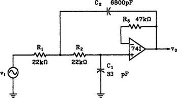
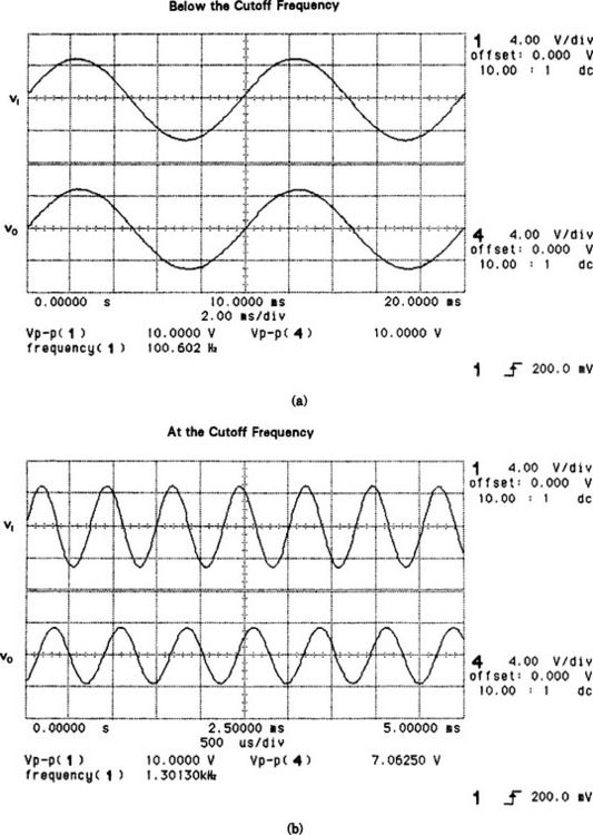

FIGURE 5.6 Actual circuit performance of low-pass filter shown in Figure 5.5. (Test equipment courtesy of Hewlett-Packard Company.)
5.3 HIGH-PASS FILTER
Figure 5.7 shows the schematic diagram of a high-pass filter circuit that provides a theoretical roll-off slope of 40 dB per decade. The circuit configuration is obtained by changing positions with all of the resistors and capacitors (except R3) in the low-pass equivalent (Figure 5.2). As a high-pass filter, we will expect it to severely attenuate signals below a certain frequency and pass the higher frequencies with minimal attenuation.

5.3.1 Operation
An intuitive feel for the operation of the circuit in Figure 5.7 can be gained by picturing the equivalent circuit at very low and very high frequencies. At very low frequencies, the capacitors will have a high reactance and will begin to appear as open circuits. Figure 5.8 shows the low-frequency equivalent circuit for the high-pass filter shown in Figure 5.7. As you can readily see, the amplifier acts as a unity gain circuit, but it has no input signal. At low frequencies, we expect little or no output signal.
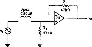
FIGURE 5.8 A low-frequency equivalent circuit for the high-pass filter shown in Figure 5.7.
At high frequencies, the capacitors will have a low reactance and will begin to appear as short circuits. The high-frequency equivalent circuit is shown in Figure 5.9. Here we see that the capacitors have been replaced with direct connections. Also, resistor R2 has been removed, because it is connected between two points that have the same signal amplitude and phase (i.e., input and output of a voltage follower). Because it has the same potential on both ends, it will have no current flow and is essentially open. The resulting equivalent circuit indicates that for high frequencies, our high-pass filter will act as a simple voltage follower.

FIGURE 5.9 A high-frequency equivalent circuit for the high-pass filter shown in Figure 5.7.
5.3.2 Numerical Analysis
Let us now extend our look at the high-pass filter shown in Figure 5.7 to a numerical analysis. There are three primary characteristics that we will want to determine:
Cutoff Frequency.
The cutoff frequency for a high-pass filter is the frequency that causes the output voltage to be 70.7 percent of the amplitude of signals in the passband (i.e., the higher range of frequencies in this case). We can determine the cutoff frequency for the circuit in Figure 5.7 by applying Equation (5.9).
For the values in our present circuit, the cutoff frequency is computed as
Filter Q.
The Q of the circuit shown in Figure 5.7 is computed with Equation (5.10).
For the values given in Figure 5.7, the Q is computed as
If the resistor values had an exact ratio of 2:1, the Q would equal 0.707 and the passband response would be maximally flat.
Input Impedance.
The input impedance of the circuit shown in Figure 5.7 varies inversely with the input frequency. The limit, however, is established by R1 in parallel with the input impedance of the voltage follower. Therefore, for practical purposes, the limit is established by the value of R1. In our present case, the minimum input impedance will be 47 kilohms.
5.3.3 Practical Design Techniques
Let us now design a high-pass filter similar to the circuit shown in Figure 5.7. We will use the following as our design goals:
| 1. Cutoff frequency | 300 hertz |
| 2. Q | 0.707 |
| 3. Input impedance | > 2000 ohms |
| 4. Highest input frequency | 5000 hertz |
Determine the R1/R2 ratio.
As indicated by Equation (5.10), the ratio of R1 to R2 determines the Q of the circuit. Let us apply Equation (5.10) to determine the required ratio for our present design.
Now we know that resistor R1 will be twice as large as R2. In general, R1 is computed with Equation (5.11).
We can pick any convenient set of values for these resistors provided they fall within the suggested range of 1.0 to 470 kilohms, and as long as R1 is larger than the minimum input impedance specified in the design criteria. For our present example, let us choose R2 as 10 kilohms. R1 is simply twice this value, or 20 kilohms.
Compute the Value of C1 and C2.
Capacitors C1 and C2 are equal in value and can be computed by applying Equation (5.9).

We will select a standard value of 0.033 microfarad for both capacitors.
Compute the Value of R3.
Resistor R3 is included to reduce the effects of the op amp bias current that flows through R1 R3 is set equal to R1 or simply
In our case, we will use a 20-kilohm resistor for R3.
Select the Op Amp.
The following op amp parameters are the most essential when designing a high-pass filter circuit:
Additionally, if it is necessary to use high-resistance values, then every effort should be made to use an op amp with low-bias currents.
Bandwidth.
When we construct a high-pass filter with an op amp, we inherently build a bandpass filter. That is, our filter circuit, by design, will attenuate all frequencies below the cutoff frequency. Ideally, all frequencies above the cutoff frequency should be passed with minimal attenuation. In practice, however, the gain of our op amp falls off at high frequencies. Thus, the very high frequencies are attenuated by the reduced gain of the op amp.
When selecting an op amp for a particular application, we must ensure that the amplifier gain is still adequate at the highest expected frequency of operation. Since the op amp is configured for unity gain, we simply need to be sure that it has a unity gain bandwidth (fUG) that is higher than the highest input frequency. In the present case, the highest input frequency is cited as 5000 hertz. Therefore, our choice of op amps must have a unity gain frequency greater than that. This should be an easy task.
Slew Rate.
The slew rate limitation of the op amp restricts the highest frequency that we can properly amplify at a given amplitude. Since the maximum input amplitude was not specified in the design goals, we will assume that the output may produce a full swing between ±VSAT. Equation (5.7) can be used to estimate the required op amp slew rate for our present application:
Both bandwidth and slew rate requirements are within the capabilities of a standard 741 op amp. Let us plan to use this device in our design.
This completes the design of our high-pass filter circuit. The final schematic is shown in Figure 5.10, and the oscilloscope plots shown in Figure 5.11 indicate the performance of the circuit. Note the varying phase shifts for different frequencies. Additionally, Table 5.2 compares the original design goals with the actual measured circuit performance. The measured cutoff frequency is somewhat higher than the original design goal, for two reasons: First, we chose to use standard values of 0.033 microfarad for the capacitors when the correct value was 0.0375 microfarad; second, the capacitors used to build the circuit were actually 0.032 microfarad (0.022 μF || 110.01 μF) because of availability. If the exact cutoff frequency is needed, then the resistors can be made variable.
TABLE 5.2
| Design Goal | Measured Value | |
| Cutoff frequency | 300 hertz | 352.8 hertz |
| Input impedance | >2000 ohms | >10 kilohms |
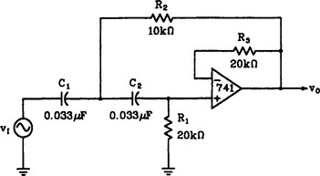

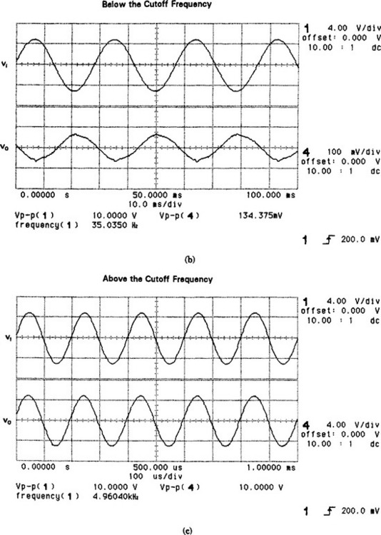
FIGURE 5.11 Actual circuit performance of the high-pass filter shown in Figure 5.10. (Test equipment courtesy of Hewlett-Packard Company.)
5.4 BANDPASS FILTER
Figure 5.12 shows the schematic diagram of a bandpass filter. This circuit provides maximum gain (or minimum loss) to a specific frequency called the resonant, or center, frequency (even though it may not actually be in the center). Additionally, it allows a range of frequencies on either side of the resonant frequency to pass with little or no attenuation, but severely reduces frequencies outside of this band. The edges of the passband are identified by the frequencies where the response is 70.7 percent of the response for the resonant frequency.
The range of frequencies that make up the passband is called the bandwidth of the filter. This can be stated as
where fH and fL are the frequencies that mark the edges of the passband. The Q of the circuit is a way to describe the ratio of the resonant frequency (fR) to the bandwidth (bw). That is,
If the Q of the circuit is 10 or less, we call the filter a wide-band filter. Narrow-band filters have values of Q over 10. In general, higher Qs produce sharper, more well-defined responses. If the application requires a Q of 20 or less, then a single op amp filter circuit can be used. For higher Qs, a cascaded filter should be used to avoid potential oscillation problems.
5.4.1 Operation
To help us gain an intuitive understanding of the circuit’s operation, let us draw equivalent circuits for the filter shown in Figure 5.12 at very high and very low frequencies. To obtain the low-frequency equivalent where the capacitors have a high reactance, we simply open-circuit the capacitors. Figure 5.13 shows the low-frequency equivalent; it is obvious from it that the low frequencies will never reach the amplifier’s input and therefore cannot pass through the filter.
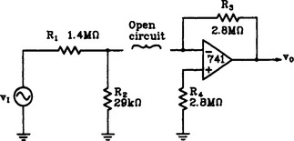
FIGURE 5.13 A low-frequency equivalent circuit for the bandpass filter shown in Figure 5.12.
At high frequencies, the reactance of the capacitors will be low and the capacitors will begin to act like short circuits. Figure 5.14 shows the high-frequency equivalent circuit, which was obtained by short-circuiting all of the capacitors. From this equivalent circuit, we can see that the high frequencies will be attenuated by the voltage divider action of R1 and R2. Additionally, the amplifier has 0 resistance in the feedback loop, which causes our voltage gain to be 0 for the op amp (i.e., no output).
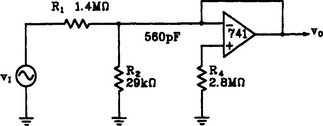
FIGURE 5.14 A high-frequency equivalent circuit for the bandpass filter shown in Figure 5.12.
At some intermediate frequency (determined by the component values), the gain of the amplifier will offset the loss in the voltage divider (R1 and R2) and the signals will be allowed to pass through. The circuit is frequently designed to have unity gain at the resonant frequency, but may be set up to provide some amplification.
5.4.2 Numerical Analysis
The numerical analysis of the filter shown in Figure 5.12 can range from very “messy” to straightforward, depending on the ratios of the components. That is, each component except R4 affects both frequency and Q of the filter. The following analytical method assumes that the filter was designed according to standard practices. The checks below will provide you with a reasonable degree of assurance that the filter design is compatible with the analytical procedure to be described:
If the answer is yes to all of these questions (which is the typical case), then the filter can be analyzed as described below. We will compute the following characteristics:
Filter Q.
The Q of the filter shown in Figure 5.12 can be computed with the following equation:
Substituting values gives us
Since the Q is less than 10, we will classify this circuit as a wide-band filter.
Resonant Frequency.
The resonant frequency of the filter shown in Figure 5.12 can be computed with the following equation:
where C is the value of either C1 or C2. Calculations for the present circuit are
It is this frequency that should receive the most amplification (or least attenuation) from the filter circuit.
Bandwidth.
The bandwidth of the filter can be calculated by applying a transposed version of Equation (5.14).
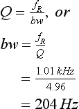
Thus, the range of frequencies that is amplified at least 70.7 percent as much as the resonant frequency is 204 hertz wide.
Voltage Gain at the Resonant Frequency.
The voltage gain at the resonant frequency can be estimated with Equation (5.17).
In the case of the circuit in Figure 5.12, the voltage gain is computed as
5.4.3 Practical Design Techniques
We are now ready to design a bandpass filter to satisfy a given design requirement. Let us design a filter similar to the circuit in Figure 5.12 that will perform according to the following design goals:
| 1. Resonant frequency | 8 kilohertz |
| 2. Q | 10 |
| 3. Voltage gain at fR | Unity |
| 4. Bandwidth | 800 hertz |
The following design is based on the assumption that the circuit provides unity gain at the resonant frequency. Although common in practice, how to design a filter to have a voltage gain of greater than unity at the resonant frequency will also be shown.
Select C1 and C2.
Although the selection of these capacitors is somewhat arbitrary, our choice of values for C1 and C2 will ultimately determine the values for the resistors. If our subsequent calculations result in an impractical resistance value, we will have to select a different value for C1 and C2 and recompute the resistance values. Because of the wide range of resistance values typically required in a given design, it is not uncommon to have resistance values ranging from 1000 ohms or less to well into the megohm ranges. Nevertheless, it should remain a goal to keep the resistance values above 1 kilohm and below 1 megohm if practical. The lower limit is established by the output drive of the op amp and the effects on input impedance. The upper limit is established by the op amp bias currents and circuit sensitivity. That is, if the resistance values are very large, then the voltage drops due to op amp bias currents become more significant. Additionally, if the resistances in the circuit are excessively high, then the circuit is far more prone to interference from outside noise, nearby circuit noise, or even unwanted coupling from one part of the filter to another. For our initial selection, let us choose to use 0.001-microfarad capacitors for C1 and C2.
Compute the Value of R1.
The value of resistor R1 is computed with Equation (5.18).
In the case of the present design, we compute the value for R1 as
We will plan to use a standard value of 200 kilohms. It should be noted, however, that the component values in an active filter are generally more critical than in many other types of circuits, so if close adherence to the original design goals is required, use either variable resistors for trimming or fixed resistors in a series and/or parallel combination, or use precision resistors.
Compute the Value for R2.
Resistor R2 is calculated with Equation (5.19).
Compute the Value for R3.
Resistor R3 is computed by simply doubling the value of R1. That is,
For our design, we compute R3 as
The nearest standard value is 390 kilohms. As previously stated, if the application requires greater compliance with the original design goals, use either a variable resistor or a combination of fixed resistors to achieve the exact value required. In our case, we will use two 200-kilohm resistors in series for R3.
Determine the Value for R4.
Resistor R4 has no direct effect on the frequency response of the filter circuit. Rather, it is included to help compensate for the effects of the op amp bias current that flows through R3. You will recall that we try to keep equal the resistances between ground and the (+) and (−) input pins of the op amp. Therefore, we will set R4 equal to R3. In equation form, we have
In this case, it is probably not necessary to use a variable resistor or fixed resistor combination to obtain an exact resistance. We will simply use the nearest standard value of 390 kilohms for R4.
Select the Op Amp.
We will pay particular attention to the following op amp parameters when selecting an op amp for our active filter:
If the resistance values turn out to be quite high, then an op amp with particularly low bias current will be important. If the capacitance values must be below about 270 picofarads, then select an op amp with minimum internal capacitances.
Bandwidth.
The required bandwidth of our op amp is determined by the highest frequency that must pass the circuit. This is, of course, the upper cutoff frequency (fH) and can be approximated (for our purposes) with Equation (5.22).
In the present case, fH is estimated as
The required bandwidth for the op amp is computed in the same manner as described in Chapter 2. It can be computed as

This is well within the capabilities of the standard 741 op amp.
Slew Rate.
The minimum slew rate for the op amp can be computed with Equation (5.7).
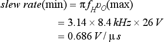
This exceeds the capability of the standard 741, which has a 0.5-volts-per-microsecond slew rate. We will use an MC1741SC for our design because it satisfies both the bandwidth and slew rate requirements of our design.
The schematic of our final design is shown in Figure 5.15. Its performance is indicated by the oscilloscope plots in Figure 5.16. Be sure to note the varying phase shifts at different frequencies. Finally, the design goals are contrasted with the actual measured performance of the circuit in Table 5.3.
TABLE 5.3
| Design Goal | Measured Value | |
| Resonant frequency | 8000 hertz | 8080 hertz |
| Q | 10 | 8.3 |
| Bandwidth | 800 hertz | 973 hertz |
| Voltage gain at fR | 1.0 | 0.825 |
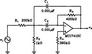

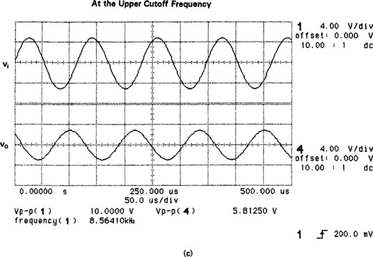
FIGURE 5.16 Oscilloscope displays showing the performance of the bandpass filter shown in Figure 5.15. (Test equipment courtesy of Hewlett-Packard Company.)
5.5 BAND REJECT FILTER
A band reject filter is a circuit that allows frequencies to pass that are either lower than the lower cutoff frequency or higher than the upper cutoff frequency. That is, only those frequencies that fall between the two cutoff frequencies are rejected or at least severely attenuated.
5.5.1 Operation
Figure 5.17 shows an active filter that is based on the common twin “T” configuration. The twin T gets its name from the two RC T networks on the input. For purposes of analysis, let us consider the lower ends of R3 and C3 to be grounded. This is a reasonable approximation, since the output impedance of an op amp is generally quite low. The T circuit consisting of C1, C2, and R3 is, by itself, a high-pass filter. That is, the low frequencies are prevented from reaching the input of the op amp because of the high reactance of C1 and C2. The high frequencies, on the other hand, find an easy path to the op amp because the reactance of C1 and C2 is low at higher frequencies.
The second T network is made up of R1, R2 and C3 and forms a low-pass filter. Here the low frequencies find C3’s high reactance to be essentially open, so they pass on to the op amp input. High frequencies, on the other hand, are essentially shorted to ground by the low reactance of C3. It would seem that both low and high frequencies have a way to get to the (+) input of the op amp and therefore to be passed through to the output. If, however, the cutoff frequencies of the two T networks do not overlap, there is a frequency (fR) that results in a net voltage of 0 at the (+) terminal of the op amp.
To understand this effect, we must also consider the phase shifts given to a signal as it passes through the two networks. At the center, or resonant, frequency (fR), the signal is shifted in the negative direction while passing through one T network. It receives the same amount of positive phase shift while passing through the other T network. These two shifted signals pass through equal impedances (R2 and XC2) to the (+) input. Thus, at any instant in time (at the center frequency), the effective voltage on the (+) input is 0. The more the input frequency deviates from the center frequency, the less the cancellation effect. Thus, as we initially expected, this circuit rejects a band of frequencies and passes those frequencies that are higher or lower than the cutoff frequencies of the filter.
The op amp offers a high impedance to the T networks, thus reducing the loading effects and therefore increasing the Q of the circuit. Additionally, by connecting the “ground” point of C3 and R3 to the output of the op amp, we have another increase in Q as a result of the feedback signal. At or very near the center frequency, very little signal makes it to the (+) input of the op amp. Therefore, very little signal appears at the output of the op amp. Under these conditions the output of the op amp merely provides a ground (i.e., low impedance return to ground) for the T networks. For the other frequencies, though, the feedback essentially raises the impedance offered by C3 and R3 at a particular frequency. Therefore, they don’t attenuate the off-resonance signals as much, which has the effect of narrowing the bandwidth or, we could say, increasing the Q.
Resistor R4 is to compensate for the voltage drops caused by the op amp bias current flowing through R1 and R2. It is generally equal in value to the sum of R1 and R2.
5.5.2 Numerical Analysis
The component values for the twin-T circuit normally have the following ratios:
Under these conditions, let us compute the following circuit characteristics:
Center Frequency.
The center frequency for the twin-T filter is the frequency that causes the reactance of C3 to equal the resistance of R3. At this same frequency, XC1 = XC2 = R1 = R2. The equation for the center frequency, then, is simply a transposed version of the basic capacitive reactance equation:
Since, at the center frequency, XC1 = R1, we can substitute R1 for XC in the preceding equation to yield our equation for the center frequency of the twin-T filter:
In the case of the circuit shown in Figure 5.17, we can compute the center frequency as follows:
On either side of the center frequency, we can expect the signals to pass with a voltage gain of nearly unity.
Input Impedance.
As with many filter circuits, the input impedance of the circuit shown in Figure 5.17 varies with frequency. The lowest impedance occurs at the higher frequencies and is approximately equal to R1, R2, and R3 in parallel. That is,
In the case of Figure 5.17, we can estimate the minimum input impedance as
5.5.3 Practical Design Techniques
Now let us design a twin-T, band reject filter to satisfy a specific design requirement. We will design a filter that will deliver the following performance:
| 1. Center frequency | 5500 hertz |
| 2. Minimum input impedance | 10 kilohms |
| 3. Highest input frequency | 18 kilohertz |
Select a Preliminary Value for R3.
The minimum value for R3 is determined by the specification for the minimum input impedance. More specifically, the minimum value for R3 is determined according to Equation (5.25).
In our present case, the minimum value for R3 is determined as follows:
The upper limit for the value of R3 is established by two factors:
The effects of op amp bias currents can be made tolerable if we keep the value of R3 below about 270 kilohms. Although the bias currents do not actually flow through R3, it is the value of R3 that will determine the values for R1 and R2. The minimum practical value for the capacitors is affected by several things, including the op amp used and the required degree of stability. A workable goal, however, is to design the circuit such that all capacitor values are greater than 100 picofarads.
Let us initially choose a value of 22 kilohms for R3. If the computed values for the capacitors are found to be too small, or there are no reasonably close standard values, then we will have to select a different value for R3 and recompute.
Determine the Value for C1.
First we compute the ideal value for C1; then we will select the nearest standard value. We can compute the required value of capacitance by applying Equation (5.26).
For the present design, we compute the value for C1 as follows:
Let us choose the nearest standard value of 680 picofarads for C1.
Compute the Exact Value for R3.
Now that a standard value for C1 has been selected, we can determine the exact value required for R3. It should be noted that the performance of the twin-T filter design relies heavily on accurate selection and matching of component values. Therefore, “ballpark” values are usually inappropriate. The exact value needed for R3 can now be computed by applying a transposed version of Equation (5.26).
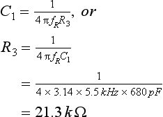
We can obtain this value by combining fixed resistances (e.g., 27 kΩ in parallel with 100 kΩ) or by using a fixed resistance and a variable resistor in series (e.g., 18-kilohm fixed resistor in series with a 5-kilohm variable resistor). In either case, however, every effort should be made to obtain the correct value.
Compute C2 and C3.
Capacitor C2 is always the same value as C1. That is,
For our purposes, we compute C2 as
Capacitor C3 is twice the size of C1, or simply
In our particular case
The nearest standard value is 1500 picofarads, which is close enough for many applications, but would undermine the performance of our filter. The simplest way to obtain more precise values in this case is to parallel two 680-picofarad capacitors. This will give us the value we need.
Compute R1 and R2.
Resistors R1 and R2 are equal in size and are twice the value of R3. We can express this as an equation.
In the present design case, we compute these resistors as
The nearest standard value is 43 kilohms. We might be able to get by with this, but in general we must try to obtain the exact values required. To this end, let us choose either a combination of fixed resistors (e.g., 39 kΩ in series with a 3.6 kΩ) or a fixed resistor and a variable resistor in combination (e.g., a 39-kΩ fixed resistor in series with a 5-kΩ variable resistor).
Compute R4.
Resistor R4 helps to compensate for the voltage drop across R1 and R2 that is produced by the op amp bias currents. To minimize the effects of the bias currents, we set R4 equal to the series combination of R1 and R2. That is,
For purposes of our present design, R4 is computed as
For many applications, this is not a critical value. In our case, let us use the nearest standard value of 82 kilohms.
Select the Op Amp.
As with previous filter designs, there are two op amp parameters that we want to focus on in order to select an appropriate op amp.
As mentioned before, if the resistance values turn out to be quite high, then an op amp with particularly low bias current will be important. And, if the capacitance values must be below about 270 picofarads, we select an op amp with low internal capacitances.
Bandwidth.
The required bandwidth of our op amp is determined by the highest frequency that must pass the circuit. The design specifications for our present case specify the highest input frequency as 18 kilohertz. The required bandwidth for the op amp is computed in the same manner as described in Chapter 2:

This is well within the capabilities of the standard 741 op amp.
Slew Rate.
The minimum slew rate for the op amp can be computed with Equation (5.7).

This exceeds the capability of the standard 741, which has a 0.5-volts-per-microsecond slew rate. We will use an MC1741SC for our design, as it satisfies the design’s bandwidth and slew rate requirements.
This completes the design of our 5500-hertz band-reject filter, whose schematic is shown in Figure 5.18. The oscilloscope displays in Figure 5.19 indicate the performance of the circuit at resonance, at the two cutoff frequencies, and at two far removed frequencies in the passband of the filter. Table 5.4 contrasts the design goals for the filter with the actual measured performance of the final design. It should be noted that 5-percent tolerance components were used to construct the circuit. More precise values would yield performance correspondingly closer to the design goals. The Q of the circuit can go as high as 40 or 50 with careful selection of components.
TABLE 5.4
| Design Goal | Measured Performance | |
| Resonant frequency | 5500 hertz | 5693 hertz |
| Minimum ZIN | 10 kilohms | 10.65 kilohms |
| Q | Not specified | 22 |
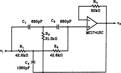


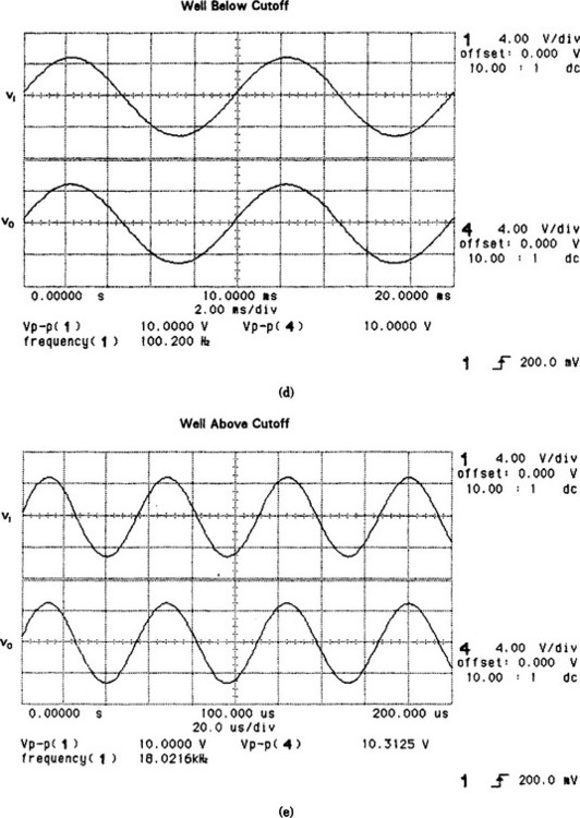
FIGURE 5.19 Oscilloscope displays showing the performance of the twin-T filter shown in Figure 5.18. (Test equipment courtesy of Hewlett-Packard Company.)
5.6 TROUBLESHOOTING TIPS FOR ACTIVE FILTERS
We can generally classify potential troubles in active filters into two broad classes:
Our first measurements will quickly tell us which type of problem exists. We can then focus our efforts on areas that might cause this type of problem.
DC Problems.
Problems that cause the output of the op amp to be at some abnormal DC level are generally located in the same manner as described in previous chapters. Basically, you need to ensure that the proper V+ and V− are present directly on the appropriate pins of the op amp. If these voltages are correct, compare the polarity of the differential input voltage (vd) with the polarity on the output pin. If the polarities contradict normal op amp behavior, then suspect the op amp; if they are correct for a normal op amp, then measure the DC level on the input to the op amp circuit. A prior stage may be sending an abnormal DC level into this stage, which makes it appear to be defective.
If all of these appear normal, then verify the integrity of the feedback circuit. If it is open, the output of the op amp will be at one of the two extremes.
AC Problems.
If the DC voltages are correct in the filter circuit, but the filter does not correctly discriminate against certain frequencies, then suspect the frequency determining components. If the resonant, or cutoff, frequencies have simply shifted slightly, you might suspect a change in component values. On the other hand, if the AC operation of the circuit has been altered dramatically, then suspect an open component. Normal DC values with abnormal AC values often point to an open capacitor or to a resistor that is isolated from DC (e.g., R3 in Figure 5.18).
As with all op amp troubleshooting tasks, it is essential that you understand the proper operation of the circuit and continuously contrast the actual performance with the known expected performance.
REVIEW QUESTIONS
1. Refer to Figure 5.2. What is the effect on circuit operation if capacitor C2 becomes open?
2. If the DC level on the output of the op amp in Figure 5.2 is normal but there are no AC signals present, is capacitor C1 open a possible cause? Explain your answer.
3. Refer to Figure 5.7. If capacitor C2 opens, will the DC level on the output of the op amp be affected? Explain.
4. If resistor R3 shorts in Figure 5.7, what is the effect on circuit operation?
5. A circuit that passes all frequencies below the cutoff frequency is called a _____ filter.
6. A circuit that rejects a very narrow band of frequencies is called a _____ filter.
7. Refer to Figure 5.12. The ratio of resistor R4 and resistor R3 establishes the gain of the amplifier. (True or False)
8. Refer to Figure 5.15. What is the effect on circuit operation if capacitor C2 becomes open?
9. Refer to Figure 5.15. What is the effect on the DC level on the output of the op amp if resistor R2 becomes shorted?
10. Refer to Figure 5.18. Which of the following defects can cause the circuit to respond like a high-pass filter?