Nonideal Op Amp Characteristics
For purposes of analysis and design in the preceding chapters, we considered many of the op amp parameters to be ideal. For example, we generally assumed the input bias current to be 0, we frequently ignored output resistance, and we disregarded any effects caused by drift or offset voltage. This approach not only greatly simplifies the analysis and design techniques, but is a practical method for many situations. Nevertheless, more demanding applications require that we acknowledge the existence of certain nonideal op amp characteristics. This chapter will describe many of these additional considerations.
10.1 NONIDEAL DC CHARACTERISTICS
We will classify the nonideal characteristics of op amps into two general categories: DC and AC. Let us first consider the effects of nonideal DC characteristics.
10.1.1 Input Bias Current
As briefly noted in Chapter 1, the first stage of an op amp is a differential amplifier. Figure 10.1 shows a representative circuit that could serve as an op amp input stage. Clearly, the currents that flow into or out of the inverting (−) and noninverting (+) op amp terminals are actually base current for the internal transistors. So, for proper operation, we must always insure that both inputs have a DC path to ground. They cannot be left floating, and they cannot have series capacitors. These currents are very small (ideally 0), but may cause undesired effects in some applications.

Figure 10.2 can be used to show the effect of nonideal bias currents. It illustrates a basic op amp configured as either an inverting or a noninverting amplifier with the input signal removed (i.e., input shorted to ground). The direction of current flow for the bias currents and the resulting output voltage polarities are essentially arbitrary, since different op amps have different directions of current flow. However, for a given op amp, both currents will flow in the same direction (i.e., either in or out). For our immediate purposes, let us assume that the arrows on the current sources indicate the direction of electron flow. We will now apply Ohm’s Law in conjunction with the Superposition Theorem to determine the output voltage produced by the bias currents. First, the noninverting bias current (with the inverting bias current set to 0) will cause a voltage drop across RB with a value of

This voltage will be amplified by the noninverting gain of the amplifier and appear in the output as
It should be noted that this voltage will be negative in our present example, since we assume that the electron flow was out of the input terminals.
Now let us consider the effect of the bias current for the inverting input. According to the Superposition Theorem, we must set the bias current on the noninverting input to 0. Having done this, we see that since no current is flowing through RB there will be no voltage across it. Therefore, the voltage on the (+) input will be truly 0 or ground. Additionally, we know that the closed-loop action of the amplifier will force the inverting pin to be at a similar potential. This means that the inverting pin is also at ground potential; recall that we referred to this point as a virtual ground. In any case, with 0 volts across RI there can be no current flow through RI. The entire bias current for the inverting input, then, must flow through RF (by Kirchhoff’s Current Law). Since the left end of RF is grounded and the right end is connected to the output, the voltage across RF is equal to the output voltage. Therefore, the output voltage caused by the bias current on the inverting pin can be computed as
Since current has been assumed to flow out of the (−) pin, we know that the resulting output voltage will be positive. Note that this is opposite the polarity of the (+) input.
Now, continuing with the application of the Superposition Theorem, we simply combine (algebraically) the individual voltages computed above to determine the net effect of the two bias currents. Since the polarities of output voltage caused by the two bias currents are opposite, the net output voltage must be
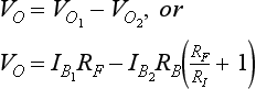
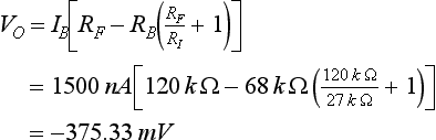
The manufacturer does not generally provide the individual values of both bias currents. Rather, the bias current (IB) listed in the specification sheet is actually an average of the two. In general, the two currents are fairly close in value, so if we assume that the two currents are equal, the preceding equation becomes
Thus, to estimate the output voltage caused by the bias currents in a particular amplifier circuit, we apply Equation (10.1). As an example, let us estimate the output voltage caused by the bias currents for the inverting amplifier circuit shown in Figure 10.3.

By referring to the data sheets in Appendix 1, we can determine the maximum value of bias current for a 741 under worst-case conditions to be 1500 nanoamperes. Substituting this into Equation (10.1) gives us
Now a good question to ask is how we design our circuits to minimize the effects of op amp bias currents. We prefer to have 0 volts in the output as a result of the bias currents, so let us set Equation (10.1) equal to 0 and then manipulate the equation.
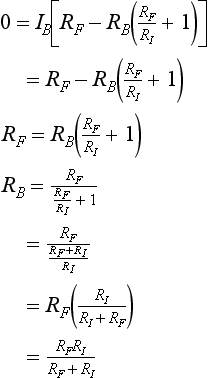
The final outcome should be recognized as an equation for two parallel resistances. You will recall that throughout the earlier chapters we always tried to set RB equal to the parallel resistance of RF and RI. This is an important result.
As a final example, let us replace RB in Figure 10.3 with the correct value and compare the results. The correct value for RB is determined with Equation (10.2).
We now apply Equation (10.1) to determine the resulting output voltage with the correct value of RB.

This, as you can see, is an improvement of over 1000 times, but you should realize that these calculations were based on the assumption that the two bias currents are identical. And while they are close, they are not truly equal. The difference between them is the subject of the next section.
10.1.2 Input Offset Current
The value of bias current listed in the manufacturer’s data sheet is the average of the two individual currents. The value listed in the manufacturer’s data sheet as input offset current is the difference between those currents, which is always less than the individual currents. In the case of the standard 741, the worst-case input offset current is listed as 500 nanoamperes (compared to 1500 nA for bias current).
The typical values for these currents at room temperature are 20 nanoamperes and 80 nanoamperes for input offset current and input bias current, respectively.
While deriving Equation (10.1), we generated the following intermediate step:
Now, from this point let us assume that RB is selected to be equal to the parallel combination of RF and RI as expressed in Equation (10.2). If we substitute this equality into this equation and then manipulate the equation, we can produce a useful expression.

Since the quantity IB1 − IB2 is the very definition of input offset current, we can make this substitution and obtain Equation (10.3).
As long as we select the correct value for RB, we can use the simplified Equation (10.3) to determine the output voltage caused by op amp input currents. In the case of the standard 741 shown in Figure 10.3 (but with the correct value for RB), the worst-case output voltage caused by offset current is
A more likely result can be found by using the typical value of offset current at room temperature. That is,
10.1.3 Input Offset Voltage
Input offset voltage is another parameter listed in the manufacturer’s data sheet. Like the bias currents, it produces an error voltage in the output. That is, with 0 volts applied to the inputs of an op amp, we expect to find 0 volts at the output. In fact, we will find a small DC offset present at the output. This is called the output offset voltage and is a result of the combined effects of bias current (previously discussed above) and input offset voltage.
The error contributed by input offset voltage is a result of DC imbalances within the op amp. The transistor currents (see Figure 10.1) in the input stage may not be exactly equal because of component tolerances within the integrated circuit. In any case, an output voltage is produced just as if there were an actual voltage applied to the input of the op amp. To facilitate the analysis of the problem, we model the circuit with a small DC source at the noninverting input terminal (see Figure 10.4). This apparent source is called the input offset voltage, and it will be amplified and appear in the output as an error voltage. The output voltage caused by the input offset voltage can be computed with our basic gain equation.
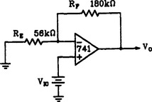
FIGURE 10.4 The input offset voltage contributes to the DC offset voltage in the output of an op amp.
The manufacturer’s data sheet for a standard 741 lists the worst-case value for input offset voltage as 6 millivolts. In the case of the circuit shown in Figure 10.4, we could compute the output error voltage caused by the input offset voltage as follows:
The polarity of the output offset may be either positive or negative. Therefore, it may add or subtract from the DC offset caused by the op amp bias currents. The worst-case output offset voltage can be estimated by assuming that the output voltages caused by the bias currents and the input offset voltage are additive. In that case, the resulting value of output offset voltage can be found as
Most op amps, including the 741, have provisions for nulling or canceling the output offset voltage. Appendix 4 shows the recommended nulling circuit for an MC1741SC. It consists of a 10-kilohm potentiometer connected between the offset null pins (1 and 5) of the op amp. The wiper arm of the potentiometer connects to the negative supply voltage. The amplifier is connected for normal operation (excluding any DC input signals), and the potentiometer is adjusted to produce 0 volts at the output of the op amp. You should realize, however, that this only cancels the output offset voltage at one particular operating point. With temperature changes or simply over a period of time, the circuit may drift and need to be readjusted. Nevertheless, it is an improvement over a circuit with no compensation.
10.1.4 Drift
Drift is a general term that describes the change in DC operating characteristics with time and/or temperature. The temperature drift for input offset current is expressed in terms of nA/°C, and the drift for input offset voltage is expressed in terms of μV/°C. The temperature coefficient of each of these quantities varies over the temperature range, and this variation may even include a change in polarity of the temperature coefficient. The maximum drift may be provided in tabular form by some manufacturers, but more meaningful data is available when the manufacturer provides a graph showing the response of input offset current and input offset voltage to changes in temperature. The data sheet in Appendix 1 is essentially a compromise between these two methods. Here the manufacturer has provided the values of input offset current and input offset voltage at room temperature and at the extremes of the temperature range.
The usual way to reduce the effects of drift is to select an op amp that has a low temperature coefficient for these parameters. Additionally, in certain critical applications some success can be achieved by including a thermistor network as part of the output offset voltage compensation network.
10.1.5 Input Resistance
An ideal op amp has an infinite input resistance. However, for practical op amps the input resistance is lower but still very high. The errors caused by nonideal input resistance in the op amp do not generally cause significant problems, and what problems may be present can generally be minimized by ensuring that the following conditions are satisfied:
1. The differential input resistance should be at least 10 times the value of feedback resistor for inverting applications.
2. The differential input resistance should be at least 10 times the values of the feedback and source resistances for noninverting applications.
In most cases, these requirements are easily met. In more demanding applications, the designer may select a FET input op amp. The MC34001 op amp made by Motorola, Inc., is an example of this type; it provides an input resistance of 1012 ohms and is pin-compatible with the standard 741 device.
10.1.6 Output Resistance
Figure 10.5 shows a circuit model that can be used to understand the effects of non-0 output resistance in an op amp. Considering that the (−) input pin is a virtual ground point, we find that RF and RL are in parallel with each other. This combination forms a voltage divider with the series output resistance (RO). The actual output voltage (VO′) will be somewhat less than the ideal output voltage (VO).
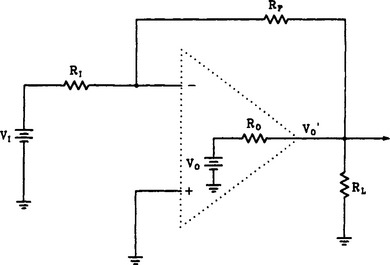
The numerical effect of RO can be determined by applying the basic voltage divider equation.
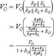
Now, as long as the following condition is maintained,
the actual output voltage will show very little loading. In practice, this condition is generally easy to satisfy. In most cases, the maximum output current of the op amp will be exceeded before the output resistance becomes a problem.
10.2 NONIDEAL AC CHARACTERISTICS
The effects of limited bandwidth have been discussed in several of the earlier chapters with reference to specific circuits. In general, the open-loop DC gain of an op amp is extremely high (typically well over 200,000). However, as the frequency of operation increases, the gain begins to fall off. At some point, the open-loop gain reaches 1. We call this the unity gain frequency, which is also referred to as the gain bandwidth product.
When the op amp is provided with negative feedback, the closed-loop gain is less than the open-loop gain. As long as the closed-loop gain is substantially less than the open-loop gain (at a given frequency), then the circuit is relatively unaffected by the reduced open-loop gain. However, at frequencies that cause the open-loop gain to approach the expected closed-loop gain, the actual closed-loop gain also begins to fall off.
We can estimate the highest operating frequency for a particular closed-loop gain as follows:
This is adequate for many, if not most, applications, but it ignores the fact that the closed-loop gain falls off more rapidly as it approaches the open-loop curve. In fact, when the circuit is operated at the frequency computed, the response will be about 3 dB below the ideal voltage gain. If this 3-dB drop is unacceptable for a particular application, then the gain must be reduced (or an op amp with a higher gain bandwidth product used).
10.2.2 Slew Rate
In order to provide high-frequency stability, op amps have one or more capacitors connected to an internal stage. The capacitor may be internal to the op amp (internally compensated), or it may be added externally by the designer (externally compensated) (Section 10.2.4 discusses compensation in greater detail). In either case, this compensating capacitance limits the maximum rate of change that can occur at the output of the op amp. That is, the output voltage can only change as fast as this capacitance can be charged and discharged. The charging rate is determined by two factors:
The charging current is determined by the design of the op amp and is not controllable by the user. In the case of internally compensated op amps, the value of capacitance is also fixed. The user does have control over the capacitance values for externally compensated op amps. The smaller the compensating capacitor, the wider the bandwidth and the faster the slew rate. Unfortunately, the price paid for this increased performance is a greater amplification of noise voltages and a greater tendency for oscillations.
Since slew rate is, by definition, a measure of volts per second, the severity of problems caused by limited slew rates is affected by both signal amplitude and signal frequency. We can determine the largest output voltage swing for a given slew rate and operating frequency by applying Equation (2.11).
Of course, we can also transpose this equation to determine the highest operating frequency for a given output amplitude.
10.2.3 Noise
The term noise, as used here, refers to undesired voltage (or current) fluctuations created within the internal stages of the op amp. Although there are many internal sources of noise, and several types, it is convenient to view the noise sources collectively as a single source connected to the noninverting input terminal. This approach to noise analysis is shown in Figure 10.6.
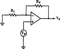
FIGURE 10.6 All of the internal noise sources in an op amp can be viewed as a single source (VN) applied to the noninverting input.
The value of the equivalent noise source shown in Figure 10.6 is labeled by some manufacturers as equivalent input noise. The gain given to this noise voltage is computed with our basic noninverting amplifier gain equation, which is
It is important to note, however, that RI for the purposes of calculating noise gain is the total resistance from the inverting pin to ground. This has particular significance in the case of a multiple-input summing amplifier, where the RI value is actually the parallel combination of all input resistors. Thus, the noise gain of the circuit is higher than any of the individual gains.
Another important aspect of noise gain is apparent when capacitance is used in the input circuit (e.g., the differentiator circuit). By having a capacitance in series with the input terminal (−), we cause the effective RI to decrease at higher frequencies, thus increasing the noise gain of the circuit.
The data sheet for the standard 741 provided in Appendix 1 shows one manufacturer’s method of providing noise specifications for an op amp. The graph labeled “Output Noise versus Source Resistance” is particularly useful. Here the manufacturer is indicating the total RMS output noise for various gains and various source resistances. The source resistor always generates thermal noise that increases with resistance and temperature. For low values of source resistance (below 1.0 kΩ), the op amp noise is the primary contributor to overall output noise. Thus, the curves remain fairly flat for various source resistance values. As the source resistance is increased beyond 10 kilohms, its noise begins to swamp out the internal op amp noise and we begin to see a steady rise in overall noise with source resistance increases.
The graph labeled “Spectral Noise Density” also provides us with greater insight into the noise characteristics of the 741. This graph indicates the relative magnitudes of noise signals at various frequencies. In particular, notice that at frequencies above 1.0 kilohertz, the distribution of noise voltage is fairly constant. This flat region is largely caused by the noise generated in the source resistance. Much of the internal op amp noise decreases with increasing frequency. By the time we reach 1.0 kilohertz, this internal noise contributes little to the overall noise signal, but below 1.0 kilohertz the overall noise amplitude increases sharply as frequency is decreased. This increase is largely caused by increased internal op amp noise and can present problems in DC amplifiers.
There are several things we can do to minimize the effects caused by noise voltages. First, we can take steps to minimize the noise gain of the circuit. This means avoiding the use of large values of feedback resistance (RF) and small values of input resistance (RI). Unfortunately, the gain of the circuit for normal signals determines the ratio of these two components, but if we bypass RF with a small capacitor, we can cause the noise gain to decrease at frequencies beyond the normal operating range of the circuit. In other words, the normal input signals will see the bypass capacitor as an open and will be unaffected, but the noise signals will see the bypass capacitor as a low impedance and reduce the overall noise gain of the circuit.
A second way to minimize the effects of noise in an op amp circuit is to ensure that the resistance between the inverting input and ground, and between the noninverting input and ground, are equal. You will recall that this same procedure helped us minimize the effects of input offset current.
Third, since the noise generated by resistors increases with resistance (actually ![]() ), we should avoid large values of resistance when noise is potentially a problem.
), we should avoid large values of resistance when noise is potentially a problem.
Finally, we can reduce the op amp’s contribution to overall output noise by selecting an op amp that is optimized for low-noise operation. The OP-27 op amp manufactured by Motorola, Inc., for example, is called an “ultra-low” noise device. It generates only 3.0 nanovolts of RMS noise at 1.0 kilohertz.
10.2.4 Frequency Compensation
We know from the study of oscillators that the two primary criteria for oscillation are in-phase (or 360°) feedback and a gain of at least unity at the feedback frequency. The op amp has a varying gain depending upon the operating frequency, but the gain requirement for oscillation is certainly a possibility.
Additionally, the op amp inherently has a 180° phase shift between its inverting input and the output by virtue of its operation. Now if we provide an additional 180° phase shift and provide a loop gain of at least unity, we will have built an oscillator.
In an earlier chapter, we provided this extra phase shift externally at a specific frequency to construct an op amp oscillator. All of the internal stages of an op amp also have certain frequency and phase characteristics. As frequency increases, the cumulative phase shift of these internal stages also increases. If, at some frequency, the total phase shift reaches 360° (or 0°) and at the same time we have a loop gain of at least unity, the circuit will oscillate even though that may not be the intended behavior.
Principles of Frequency Compensation.
So far in the text we have primarily focused on the frequency characteristics of the op amp with only occasional reference to the phase characteristics. Figure 10.7 shows a simple RC circuit and graphs showing its frequency and phase performance. Table 10.1 shows this same data in tabular form.

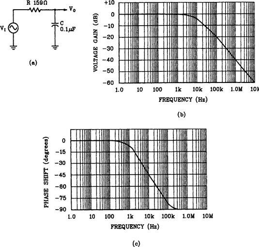
There are several things to be observed from these data. First note that the break (or cutoff) frequency occurs at 10 kilohertz. At this frequency, XC = R, the voltage gain is 0.707, and the phase shift is about 45°. Now notice that if we are at least a decade lower than the break frequency, the following occurs:
1. Voltage gain remains fairly constant (near unity).
As the cutoff frequency is passed things change. By the time we are one decade above the cutoff frequency and continuing beyond, the following occurs:
1. Voltage gain decreases by a factor of 10 for each decade increase in frequency.
2. The dB-per-decade drop continues at about −20 dB per decade.
If we add a second RC section to the circuit shown in Figure 10.7, these effects are magnified. That is, for frequencies well below both break frequencies, the circuit behaves as described for low frequencies. For frequencies greater than the break frequency of one RC section, but less than the second, the circuit response is as described for high frequencies. Finally, when the operating frequency is higher than both break frequencies, the following effects occur:
1. Voltage gain decreases by a factor of 100 for each decade increase in frequency.
This two-stage response is shown graphically in Figure 10.8 as a solid line. The dotted curves represent the responses of the individual RC sections. A similar cumulative effect occurs for each subsequent RC section added.

As briefly mentioned earlier in this section, each of the internal stages of an op amp have frequency and phase characteristics similar to the RC sections presented. Figure 10.9 shows the open-loop frequency response of a hypothetical amplifier with no frequency compensation. This response presents us with “good news” and “bad news.” The good news is that we have a substantial increase in bandwidth relative to a compensated op amp (e.g., the standard 741 shown as a dotted curve). The bad news is that the multiple break frequencies will certainly cause greater than 180° of phase shift. This internal shift coupled with the inherent 180° shift from the inverting input terminal will make this particular op amp very prone to oscillation. Now, let us determine how prone.

If we superimpose the closed-loop gain response on the open-loop response originally shown in Figure 10.9, we get Figure 10.10, where the closed-loop responses for several gains are shown. Now, the important characteristic for stability (i.e., no oscillations) is summarized in the following statement:
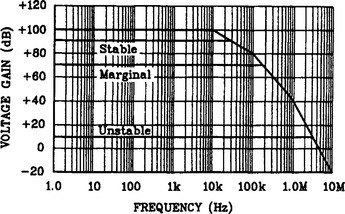
FIGURE 10.10 To ensure against oscillations, the intersection of the closed-loop gain and the open-loop gain curves must occur with a net slope of less than 40 dB per decade.
If this rule is violated, unstable operation is assured. On the other hand, if this rule is faithfully followed, it is still possible to construct an unstable amplifier circuit. Nevertheless, it provides us with an excellent starting point. We will consider exceptions at a later point in the discussion.
One method for verifying amplifier stability using this method relies on the use of simple sketches plotted on semilog graph paper. The logarithmic scale is used to plot frequency, and the linear scale is used to plot voltage gain expressed in dB. In this way, it is a simple matter to determine the net slope at the point of intersection between the closed- and open-loop gain curves. Although valid in concept, this method is often difficult to implement because the manufacturer may not provide adequate data regarding the uncompensated open-loop response. More often the manufacturer provides a set of curves that indicate the overall open loop response with frequency compensation (either internal or external). The designer must interpret these graphs to ascertain safe operating regions.
In any case, Figure 10.10 clearly indicates that the tendency for oscillation becomes greater as the closed-loop gain of the circuit is reduced. The worst-case gain, with regard to stability, occurs for 100-percent feedback or unity voltage gain. If the circuit is stable for unity gains, then we can be assured of stability at all other higher gains.
Internal Frequency Compensation.
Many general-purpose op amps (e.g., the 741 or the MC1741SC) are internally compensated to provide stability for all gains down to and including unity. This is generally accomplished by adding a capacitor to one of the internal stages, which causes the overall response to have an additional roll-off characteristic (like adding another series RC section). The break frequency of this added circuit is chosen to be lower than all other break frequencies present in the output response, defining it as the dominant network. Figure 10.11 illustrates how the response curve of an uncompensated op amp is shifted downward by the introduction of a compensation capacitor. Notice that the effects of each of the break frequencies are still present in the response but that the amplifier gain falls below unity before the slope exceeds 40 dB per decade. While this does ensure maximum stability, it is clearly detrimental to the bandwidth of the amplifier.

FIGURE 10.11 Adding a compensation capacitor increases stability but reduces the bandwidth of an amplifier.
The internal capacitance, called a lag capacitor, can be connected to any one of several points within the op amp. Since larger values of capacitance are required for lower impedance points, it is common to connect the lag capacitor at a high-impedance point in the device. Additionally, by inserting the capacitor in one of the earlier stages rather than in the output stage, it has less of a slowing effect on the slew rate. Probably the most common value of internal compensating capacitance is 30 picofarad. It can be readily identified on the simplified schematic of the standard 741 included in Appendix 1.
External Frequency Compensation.
Although the inclusion of an internal compensating capacitor greatly simplifies the use of an op amp and makes it less sensitive to sloppy designs, it does cause an unnecessarily severe reduction in the bandwidth of the circuit. Alternatively, the manufacturer may elect to bring out one or more pins for the connection of an external compensating capacitor. The value of the capacitor can be tailored by the designer for a specific application.
The extreme case, of course, is to put heavy compensation on the device to make it stable all the way down to unity gain. This makes the externally compensated op amp equivalent to the internally compensated one. However, many applications do not require unity gain. In these cases, we can use a smaller compensating capacitor, which directly increases the bandwidth. So long as the closed-loop gain curve intersects the open-loop gain curve with a net slope of less than 40 dB, we will generally have a stable circuit.
The LM301A op amp is an externally compensated, general-purpose op amp. Its data sheet includes a graph that illustrates the effect on open-loop frequency response for compensating capacitors of 3 and 30 picofarads. A second graph shows the dramatic increase in large-signal frequency response obtained by using a 3-picofarad capacitor instead of a 30-picofarad. With a 30-picofarad capacitor, the full-power bandwidth is limited to about 7.5 kilohertz (nearly the same as a standard 741). By using 3-picofarad, however, the full-power bandwidth goes up to about 100 kilohertz. This can be attributed to an increased slew rate. It should be noted that 3 picofarads is a very small capacitance. This value can easily be obtained or even exceeded by stray wiring capacitance.
The negative side, however, is evident in the open-loop frequency response. The curve for 3 picofarads does not extend to unity gain (0 dB). That is, we must design the circuit to have substantial (e.g., 40-dB) gain to insure stability.
Feed-Forward Frequency Compensation.
The lowest, and therefore most dominant, break frequency in an uncompensated op amp is generally caused by the frequency response of the PNP transistors in the input stage. Although this stage does not provide a voltage gain, the attenuation to the signal increases with frequency. By connecting a capacitor between the inverting input and the input of the next internal stage, we can effectively bypass the first stage for high frequencies, thus boosting the overall frequency response of the op amp. This technique is called feedforward compensation.
The manufacturer must provide access to the input terminal of the second stage in order to employ feedforward compensation. In the case of the LM301, feedforward compensation is achieved by connecting a capacitor between the inverting input and pin 1 (balance). Examination of the internal schematic will reveal that this effectively bypasses the NPN differential amplifier on the input and the associated level-shifting PNP transistors.
When feedforward compensation is used, a small capacitor must be employed to bypass the feedback resistor to ensure overall stability. The manufacturer provides details for each op amp that demonstrate the selection of component values.
The use of feedforward compensation produces all of the following effects:
10.2.5 Input Resistance
Calculation of input resistance, or, more correctly, input impedance, was presented in Chapter 2. In the case of a noninverting configuration, we found that the open-loop input resistance of the op amp is magnified when the feedback loop is closed. Equation (2.29) is used to determine the effective input impedance once the loop is closed.
This calculation, of course, produces a very high value, which for most applications can be viewed as the ideal value of infinity.
In the case of an inverting configuration, the input impedance is generally considered to be equal to the value of the input resistor. That is, the impedance directly at the inverting input is generally considered to be 0 (virtual ground). This approximation is satisfactory for most applications. If a greater level of accuracy is needed, we can estimate the actual input impedance directly at the inverting input with Equation (10.5).
The total input impedance for the amplifier circuit is simply the sum of the input resistor and the value computed with Equation (10.5).
10.2.6 Output Resistance
The calculation and effects of output resistance, or impedance, were presented in Chapter 2. There it was found that the closed-loop output resistance was substantially reduced from the open-loop value. Equation (2.15) was used to estimate the closed-loop output impedance for either inverting or noninverting configurations:
This is an adequate approximation for most applications. In the case of very low open-loop gains (e.g., at higher frequencies), Equation (10.6) provides a more accurate estimate of the closed-loop output impedance.
In most cases, the finite output resistance has little effect on circuit operation. The maximum output current capability will generally limit the size of load resistor to a value that is still substantially larger than the output resistance of the op amp. Therefore, the voltage divider action of output resistance is minimal.
10.3 SUMMARY AND RECOMMENDATIONS
For some applications, many of the nonideal characteristics of op amps can be ignored without compromising the design. But how do you know which parameters are important under what conditions? The answer to that question is quite complex, but the following will provide you with some practical guidelines.
10.3.1 AC-Coupled Amplifiers
If a particular amplifier is AC-coupled (e.g., capacitive-, optically-, or transformer-coupled), then the nonideal DC characteristics can often be ignored. Any offsets caused by bias currents, drift, and so on, will be noncumulative; that is, the effects will be limited to the particular stage being considered and will not upset the operation of subsequent stages. Therefore, as long as the DC offset is not so great as to present problems (e.g., saturation on peak signals) in the present stage, it can probably remain uncompensated.
Frequency response and slew rate, on the other hand, are important in nearly every AC-coupled application. These parameters should be fully evaluated before a particular amplifier is selected for a given application.
Noise characteristics can often be ignored, but it depends on the application and on the amplitude of the desired signal relative to the noise signal. If the noise signal has an amplitude that is comparable to the desired signal, then the designer should take steps (discussed in an earlier section) to minimize the circuit noise response. On the other hand, if the primary signal is many times greater than the noise signal, the design may not require any special considerations with regard to noise reduction.
10.3.2 DC-Coupled Amplifiers
DC-coupled amplifiers seem to present some of the more formidable design challenges. Depending on the specific application, a DC amplifier may be affected by literally all of the nonideal op amp characteristics. This is certainly the case for a DC-coupled, low-level, wideband amplifier.
If, however, the input frequency is always very low (e.g., the output of a temperature transducer), then considerations regarding slew rate and bandwidth can often be disregarded. In these cases, the emphasis needs to be on the DC parameters such as DC offsets and drifts.
10.3.3 Relative Magnitude Rule
A good rule of thumb that is applicable to all classes of amplifiers and to all of the nonideal characteristics of op amps involves the relative magnitude of the nonideal quantity compared to the desired signal. If the nonideal value is less than 10 percent of the desired signal quantity, then ignoring it will cause less than a 10 percent error. Similarly, keeping the nonideal value below 1 percent of the desired signal will generally keep errors within 1 percent even if the nonideal quantity is disregarded.
Consider, for example, the case of input bias current. If the input bias current is approximately 700 microamperes and the input signal current is expected to be 1.2 milliamperes, then to ignore bias current would be to make a significant error because the bias current is comparable in magnitude to the desired input current.
Now suppose that the cumulative effects of bias current and input offset voltage for a particular amplifier are expected to produce a 75-millivolt offset at the output of the op amp. If the normal output signal is a 1-volt sinewave riding on a 5-volt DC level, then the undesired 75 millivolts offset can probably go unaddressed without producing any serious effects on circuit operation.
10.3.4 Safety Margins on Frequency Compensation
It is common to speak of phase margin and gain margin with reference to op amp frequency compensation. The terms describe the amount of safety margin between the designed operating point of the op amp and the point where oscillations will likely occur. The absolute limits (i.e., zero safety margin) occur when the closed-loop gain reaches unity and has a phase shift of −180°. This is the dividing line between oscillation and stable operation.
Gain margin is defined as the difference between unity and the actual closed-loop voltage gain at the point where a −180° phase shift occurs. To insure stable operation and to allow for variances in component values, the loop gain should fall to about one-third or −10 dB by the time the phase shift has reached −180°. Similarly, the phase margin is the number of degrees between the actual phase shift and −180° at the time the loop gain reaches unity. A safety margin of about 45° is recommended. If these safety margins are maintained and the capacitive loading on the output of the amplifier is light, then the circuit should be stable and perform as expected.
REVIEW QUESTIONS
1. The value of the difference between the two input bias currents of an op amp is provided by the manufacturer in the data sheet and is called ____.
2. Drift is a nonideal characteristic that primarily affects (AC-coupled/DC-coupled) op amp circuits.
3. What type of op amp would you select if a very high value of input impedance was required?
4. Noise generation in op amp circuits can be reduced by selecting very large values of resistance. (True or False)
5. If the intersection of the closed-loop gain curve and the open-loop gain curve for an op amp amplifier occurs with a net slope of 60 dB per decade, will the amplifier be stable? Explain your answer.