Power Supply Circuits
6.1 VOLTAGE REGULATION FUNDAMENTALS
Nearly all electronic systems require one or more sources of stable DC voltage. Yet many systems get their input power from the standard 120-VAC power line. Even battery-powered units may require stable DC voltages at levels other than those provided directly by the battery. Figure 6.1 shows the basic role played by a voltage regulator circuit and where it fits in the power distribution scheme.

If the system receives its power from the 120-VAC power line, the first step is usually voltage reduction via a step-down transformer. The output of the transformer (there may be more than one) is then rectified to produce pulsating DC. The rectified waveform is then filtered with large capacitors to produce a relatively smooth but unregulated source of DC voltage. An unregulated voltage source is one that varies with changes in load current or in applied voltage. All of the functions just described are represented by the first block in Figure 6.1.
The voltage at the output of the rectifier/filter is smooth DC, but it is not regulated. Thus, the value of voltage will change with changes in input voltage or with changes in load current. To eliminate these changes and produce a solid source of DC voltage, we route the filtered DC to a voltage regulator circuit (the second block in Figure 6.1).
There are many types of voltage regulator circuits, but the purpose remains the same—to maintain a constant output voltage even though both the input voltage and the load current may be changing. The regulated output voltage is always less than the unregulated input voltage.
We will examine three basic classes of voltage regulator circuits:
6.1.1 Series Regulation
Figure 6.2 illustrates the basic concept of series voltage regulation. The voltage regulator circuit is designed to act as a variable resistance in series with the load. The regulator senses changes in load voltage (whether caused by changes in input voltage or by changes in load current) and adjusts its resistance such that the voltage across the load remains constant. This is one of the most common voltage regulation techniques. The regulator can also be designed to protect against short circuits on the regulated output. In practice, the “variable resistor” shown as the regulating element in Figure 6.2 is actually a transistor or an integrated voltage regulator circuit.

6.1.2 Shunt Regulation
The concept of a shunt-voltage regulator is illustrated in Figure 6.3. Here the regulating element (shown as a variable resistor) is connected in parallel, or shunt, with the load. The regulator circuit senses changes in load voltage and adjusts the effective resistance of the regulating element to compensate. If, for example, the load current drops, the output voltage tends to rise (i.e., less drop across RS). The regulator circuit detects this change, however, and decreases the resistance of the shunt regulator element, causing the regulator branch to draw more current and the current through RS to remain constant, and preventing the output voltage from rising.
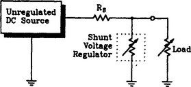
The shunt regulator is generally used for low-current applications because it consumes a significant amount of power. A simple zener diode is an example of a shunt regulator. By adding an op amp, however, the degree of regulation can be improved.
6.1.3 Switching Regulation
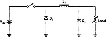
The basic operation of a switching voltage regulator circuit is shown in Figure 6.4. Here, the regulating element (usually a transistor) is operated either full on (closed switch) or full off (open switch). The switching usually occurs at tens or hundreds of kilohertz.

While the switch is closed, the unregulated source supplies current to the load via L1. The inductance of L1 smooths the current changes that might be caused by the switching circuit. During this time, energy is stored in the magnetic field that builds up around the coil. When the switch opens, the magnetic field begins to collapse and the stored energy is returned to the circuit. The collapsing field now acts as a voltage source and keeps the load current flowing steadily through the alternate path of D1.
Many switching regulator circuits adjust the duty cycle of the switching action to compensate for changing load or input voltage conditions. That is, if the on time of the switching action is lengthened (relative to the off time), the average (DC) output voltage will be higher. As with the other regulator circuits, the switching regulator must sense changes in the output voltage in order to compensate (i.e., regulate).
6.1.4 Line and Load Regulation
In order to express the regulator’s ability to compensate for changes in the line voltage or the load current, we compute two percentages. The first, called line regulation, provides an indication of the regulator’s ability to compensate for changes in the input voltage. It is a simple ratio of the change in output voltage to the change in line voltage. That is,
The second percentage, called load regulation, provides an indication of the regulator’s ability to compensate for changes in load current. It is computed as
6.1.5 Voltage References
All of the regulator circuits described in this chapter require a stable reference voltage. The actual load voltage is continuously compared against this reference to determine what changes are required by the regulator circuit. In essence, the voltage reference is in itself a voltage regulator circuit.
Although a zener diode is a low-cost, practical reference source, the actual zener voltage changes significantly with changes in current through the zener. Therefore, if we want a more stable source, we must go beyond the simple zener regulator. Figure 6.5 shows a circuit that combines a zener diode and an op amp to produce a simple but stable reference voltage. We will utilize this circuit in all of the regulator circuits described in this chapter.

FIGURE 6.5 A simple, but stable, voltage reference can be built around a single-supply op amp and zener diode.
The MC3401 op amp is somewhat different than the other op amps discussed so far in the text. It is designed for operation from a single power supply—that is, only one power source is required for normal operation. A more complete discussion of single-supply op amps is presented in Chapter 11. For now, suffice it to say that the input terminals are essentially PN junctions connected to ground. This means that the voltage on either input will remain at 0.6 volts or less. You may think of the input as responding to current changes in the same way as the emitter-base circuit of a transistor.
Since the voltage across R1 is constant (approximately 0.6 volts), its current is constant. It is essentially equal to the zener diode current because the op amp bias current is insignificant. Since the zener current is constant, the zener voltage will be constant.
If the output voltage attempts to change, this change is felt on the (−) pin via D1. Because the voltage on the (−) input is essentially limited by an internal junction, the changes fed back have only minimal effect on the voltage on the (−) pin, but rather cause changes in bias currents. In any case, the result is that the output of the op amp changes in a polarity that tends to compensate for the changing output voltage. All of this closed-loop action occurs almost instantly, so the actual load voltage never really changes significantly. Although the circuit compensates for changes in load current and in input voltage, it may still drift as a result of changes in temperature. This latter effect can be essentially eliminated by selecting a zener diode with a temperature coefficient that is opposite (+2 mV/°C) from that in the op amp. For our purposes, we will ignore the effects of temperature changes.
The output or reference voltage for the circuit shown in Figure 6.5 can be approximated with Kirchhoff’s Voltage Law. That is,
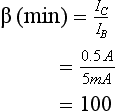
Transistor Q1 is a simple current booster (as discussed in Chapter 2). The output current of the op amp is limited to about 5 milliamperes, but required zener currents may be substantially higher than this. Assuming that the junction breakdown voltages are adequate, there are only three critical parameters for the selection of Q1:
The minimum required current gain for Q1 can be determined from the basic transistor equation for current gain,
where 5 milliamps is the maximum recommended output current for the MC3401 op amp.
The power dissipation for Q1 can be determined from the basic power equation.
Resistor R1 simply establishes the desired zener current. Ohm’s Law gives us an approximate value.
Let us now design a voltage reference to be used as a stable source for the regulator circuits presented in this chapter. We use the following design goals:
| 1. Unregulated input voltage | +10 to 15 volts DC |
| 2. Regulated output voltage | +4 volts |
| 3. Percent of voltage regulation | 0.1 percent |
| 4. Maximum reference current | 1 milliampere |
Choose D1.
The required voltage for D1 can be determined by applying Equation (6.1). In our case
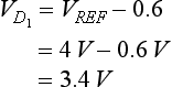
This is not necessarily the value of the zener diode. Rather, it is the required voltage across it. We will refer to a manufacturer’s data sheet (Appendix 5) and select a diode that is close to the required voltage and then adjust the zener current to obtain the exact value needed. For the present case, let us choose a 1N5227 zener, which is rated for 3.6 volts when a 20-milliampere current is passed through it. We will adjust the value of R1 to cause more or less current through the zener and therefore obtain a higher or lower voltage drop across it. Recall that the zener voltage varies nonlinearly with zener current, and that the exact zener voltage at a certain current varies between similar devices. Although the exact value for R1 will have to be obtained experimentally, the circuit is exceptionally stable once it is constructed.
Compute R1.
We can now calculate a starting value for R1 with Equation (6.4).
We will use a standard value of 27 ohms for R1. Once the circuit has been constructed, we may have to adjust R1 slightly to obtain the exact output voltage.
Select Q1.
Because the highest DC input voltage was listed as +15 volts, our collector-to-emitter and collector-to-base breakdown voltages should be greater than 15 volts. The minimum current gain is computed with Equation (6.2).
This, of course, is not a challenging goal. In fact, if the actual zener current were less than 5 milliamps, we could omit Q1 from the design.
The power dissipation for Q1 can be estimated with Equation (6.3) as

Finally, Q1 must be able to handle the combined currents of IZ and IREF as collector current. In our particular case,
Let us choose a common 2N2222A as the current booster for our design. The data sheet in Appendix 3 indicates that it will exceed our requirements. By following the process presented in Appendix 10, we can determine that no heat sink will be necessary, but the transistor will operate fairly hot. It might be desirable to add a small heat sink.
Figure 6.6 shows the final schematic of our 4-volt reference circuit. The input and output voltage levels are shown on the oscilloscope displays in Figure 6.7 for minimum and maximum input voltage conditions. Finally, Table 6.1 contrasts the actual circuit performance with the original design goals.
TABLE 6.1
| Design Goal | Measured Value | |
| Input voltage (DC) | +10–15 volts | +10–15 volts |
| Output voltage (VREF) | +4 volts | +3.985 volts |
| Percent regulation | 0.1 percent | 0.004 percent |
| Reference current | 0–1 milliamperes | 0–1 milliamperes |

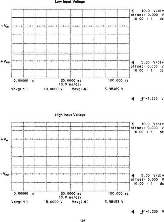
FIGURE 6.7 Oscilloscope displays showing the stability of the voltage reference shown in Figure 6.6. (Test equipment courtesy of Hewlett-Packard Company.)
As Table 6.1 and the oscilloscope displays in Figure 6.7 indicate, the actual circuit performance exceeds our design requirements. Be sure to note in Figure 6.6 that the actual value of R1 was adjusted to 22 ohms to trim the output voltage to the required value.
6.2 SERIES VOLTAGE REGULATORS
Figure 6.8 shows the schematic diagram of a basic series regulator circuit. The input to the circuit is filtered but unregulated DC voltage; the output, of course, is regulated DC voltage that remains constant in spite of changes in the load current or changes in the input voltage.
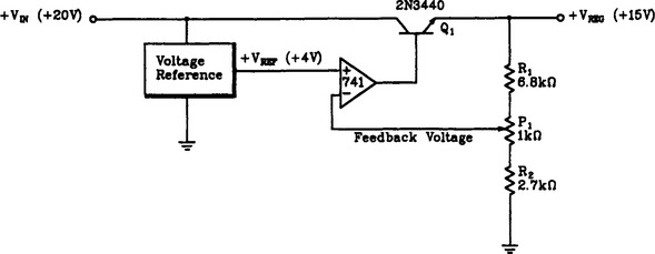
Transistor Q1 in Figure 6.8 is known as the series pass transistor. Kirchhoff’s Voltage Law tells us that the voltage across the load plus the voltage across the series-pass transistor must always be equal to the applied voltage. Thus, if we can control the amount of voltage dropped across the pass transistor, we have inherent control over the load voltage.
The output voltage of the regulator circuit is sampled with the voltage divider made up of resistors R1, R2, and potentiometer P1. The portion of the output that appears on the wiper arm of P1 is called the feedback voltage. Potentiometer P1 is used to adjust the amount of feedback voltage and thus is used to adjust the output voltage level.
The voltage reference circuit indicated in Figure 6.8 was discussed in an earlier section. Its purpose is to provide a constant voltage level that can be used as a stable reference. The schematic of a representative voltage reference circuit was presented in Figure 6.5.
The op amp in Figure 6.8 is called the error amplifier. It continuously compares the magnitude of the reference voltage with the level of the feedback signal (which represents the output voltage). Any difference between these two voltages (both magnitude and polarity) is amplified and applied to the base of the pass transistor. The polarity is such that the output voltage is returned to its correct value. As an example, let us assume that the load current suddenly decreases, which tends to make the output voltage rise. However, as soon as the output voltage starts to increase (i.e., become more positive), the feedback voltage on the wiper arm of P1 also becomes more positive. This increasing positive on the inverting pin of the op amp causes the output of the op amp to become less positive (i.e., moves in the negative direction). Recall that the reference voltage remains constant, so any changes in the feedback voltage are immediately reflected in the output of the op amp. This reduced positive voltage on the base of Q1 reduces the amount of forward bias and therefore increases the effective resistance of the pass transistor, causing an increased voltage drop across it. Because we are now dropping more voltage across the pass transistor, we will have less dropped across the load (Kirchhoff’s Voltage Law). Thus, the initial tendency for the load voltage to rise has been offset by an increased voltage drop across the pass transistor. This process happens nearly instantaneously so that the load voltage never really sees a significant increase. Of course, the better the degree of regulation, the smaller the changes in load voltage.
To further clarify the operation of the error amplifier, let us examine the circuit from a different viewpoint. First, consider the wiper arm to be at some fixed point. We can now view the resistor network as a simple, two-resistor voltage divider. A redrawn circuit for the error amplifier is shown in Figure 6.9. Here R1′ is equivalent to R1 and that portion of P1 above the wiper arm. Similarly, R2′ is equivalent to R2 and that portion of P1 below the wiper arm. It is readily apparent that the resulting circuit is a simple noninverting amplifier circuit with a current boost transistor. This circuit was discussed in detail in Chapter 2.
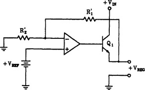
FIGURE 6.9 A simplified circuit of the error amplifier portion of Figure 6.8. It is actually a simple noninverting voltage amplifier with a current boost transistor.
Potentiometer P1 in Figure 6.8 is used to adjust the output voltage to a particular level. If we move the wiper arm up, we increase the feedback voltage (i.e., more positive), decrease the bias on Q1, increase the voltage drop across Q1, and ultimately bring the output voltage down to a new, lower level. Similarly, if we move the wiper arm down, we reduce the amount of feedback voltage (i.e., less positive), increase the bias on Q1, decrease the voltage drop across Q1, and cause the load voltage to increase to a higher regulated level.
It is important to note that the series-regulator circuit shown in Figure 6.8 is not immune to short circuits. That is, if the output of the regulator was accidentally shorted to ground, the pass transistor would undoubtedly be destroyed by the resulting high-current flow. Many, if not most, regulated supplies are designed to be current limited. Section 6.5 discusses this option in greater detail.
6.2.2 Numerical Analysis
Let us now analyze the series-voltage regulator circuit presented in Figure 6.8. The output voltage of the regulator can be computed with Equation (6.5).
where R1′ and R2′ are the equivalent values shown in Figure 6.9 and as discussed. If we assume that the wiper arm of P1 is moved to the uppermost extreme, we can apply Equation (6.5) to compute the minimum output voltage as shown:

Similarly, we can move the wiper arm to the lowest position and compute the highest output voltage with Equation (6.5) as follows:

So the range of regulated output voltages that can be obtained by adjusting P1 is 11.36 through 15.56 volts.
The maximum allowable output current is determined by one of the following:
Whichever of these limitations is reached first will determine the maximum allowable current that can be drawn from the regulator output.
The manufacturer’s data sheet for a 2N3440 lists the maximum collector current as 1.0 amp. The data sheet also lists the maximum power dissipation as 1.0 watt (at 25°C), gives a thermal resistance from junction to case as 17.5°C per watt, and lists the thermal resistance from junction to air as 175°C per watt. No current limit is shown in Figure 6.8 for +VIN. The current limit imposed by the power rating can be computed as follows:
where PD is the maximum power as determined with Equation (A10.3) in Appendix 10. In the case of the circuit shown in Figure 6.8, the current limit imposed by the power rating of the transistor (for TA = 40°C) is computed as
Since this current is lower than the 1.0-amp maximum collector current rating, it will be the limiting factor. Thus, the regulator circuit shown in Figure 6.8 has a maximum output current of about 105 milliamperes.
6.2.3 Practical Design Techniques
Let us now design a series-voltage regulator similar to the one shown in Figure 6.8. We will use the following as design goals:
| 1. Input voltage | +12 to +18 volts |
| 2. Output voltage | +6 to 9 volts |
| 3. Output current | 0 to 0.5 amps |
| 4. Line regulation | <1 percent |
| 5. Load regulation | <1 percent |
| 6. Error amplifier | 741 |
Select the Pass Transistor.
The characteristics of the pass transistor are determined by the input voltage, the output voltage and current requirement, and the output drive capability of the op amp. First, the collector current rating of the transistor must be greater than the value of load current. In our case, this means that our transistor must have a maximum DC current rating of greater than 500 milliamperes.
The transistor power dissipation can be found by applying Equation (6.6).
The minimum current gain (hFE or β) for the transistor can be found by applying our basic transistor formula for current gain:
With a circuit like that shown in Figure 6.8, base current is provided by the output of the op amp. We will establish the maximum current to be provided by the op amp as one-fourth of the short-circuit output current rating of the op amp, which, in the case of a 741, is listed in the data sheet as 20 milliamperes. Therefore, we shall limit the output current (and therefore the base current of Q1) to one-fourth of 20 milliamperes, or 5 milliamperes. The minimum current gain for Q1 can now be determined as shown:
The minimum collector-to-emitter voltage breakdown rating for Q1 is found by determining the maximum voltage across Q1. That is,
In our particular case, the collector-to-emitter voltage rating is computed as
There are many transistors that will satisfy the requirements for Q1. Let us select an MJE1103 (refer to Appendix 2) for this application. The calculations presented in Appendix 10 indicate that the transistor will require a heat sink for safe operation.
Determine the Required Op Amp Voltage Gain.
The equivalent circuit shown in Figure 6.9 is useful for determining the required voltage gain of our op amp. We must consider the circuit under both minimum and maximum output voltage conditions. The minimum and maximum voltage gains are determined from the basic amplifier gain formula (AV = VO/VI). That is,
In our present application, the required voltage gains for the op amp are determined as follows:

Select the Value for P1.
Selection of P1 is largely arbitrary, but some guidelines may be established. Its minimum value should be at least 20 times the minimum equivalent load resistance. That is,
In our particular case, the minimum recommended value for P1 is
The maximum value is also somewhat arbitrary, but there is generally no reason for going beyond a few tens of thousands of ohms. Let us decide to use a 5-kilohm potentiometer for P1 in this particular application.
Compute R1 and R2.
The values for R1 and R2 can be determined by applying the basic equation for voltage gain in a noninverting amplifier (refer to Figure 6.9). Recall that minimum voltage gain occurs when the wiper arm of P1 is at its upper extreme. Under these conditions, the equation for R1 can be determined as follows:
Similarly, an equation for R2 can be derived from the basic gain equation as shown:

Substituting Equation (6.11) for R1 in this equation and performing some algebraic transposing gives us our final equation for the value of R2.
We can now compute the required values for R1 and R2. First, we apply Equation (6.12) to find R2.
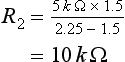
We are now in a position to apply Equation (6.11) to find the value of R1.

Because the computed values for R1 and R2 are both standard, we do not have to make any decisions regarding standard values. For most applications, we simply choose the nearest standard value.
This completes the design of our series regulator circuit. The final schematic is shown in Figure 6.10, and the performance of the circuit is indicated by the oscilloscope displays in Figure 6.11. The waveforms show the effects of minimum and maximum load current and minimum and maximum line voltage. Figure 6.11(a) shows the output under no-load conditions, and Figure 6.11(b) illustrates the effect of adding a 500-milliampere load. In both cases, the output voltage was adjusted to minimum (+6 volts). Figure 6.11(c) shows the results of maximum input voltage under no-load conditions; finally, Figure 6.11(d) illustrates the circuit performance under conditions of maximum input voltage and a 500-milliampere load. The measured performance of the circuit is summarized and contrasted with the original design goals in Table 6.2.
TABLE 6.2
| Design Goal | Measured Value | |
| Input voltage | +12 to +18 volts | +12 to +18 volts |
| Output voltage | +6 to +9 volts | +5.97 to +9.07 volts |
| Output current | 0 to 500 milliamperes | 0 to 500 milliamperes |
| Load regulation | <1 percent | 0.99 percent |
| Line regulation | <1 percent | 0.56 percent |
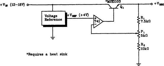
FIGURE 6.10 A series voltage regulator circuit designed to deliver 6 to 9 volts at 0 to 500 milliamperes.

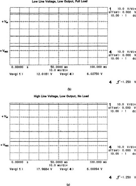
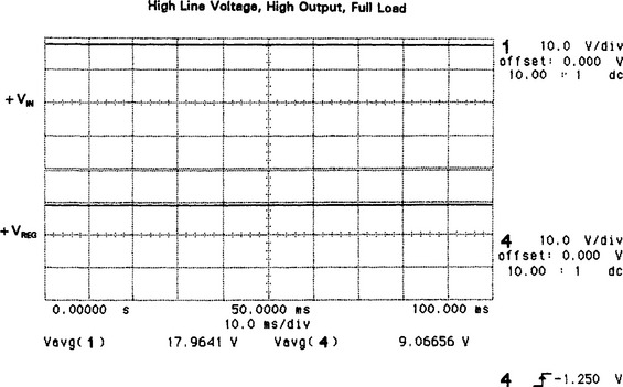
FIGURE 6.11 Oscilloscope displays showing the performance of the series voltage regulator shown in Figure 6.10. (Test equipment courtesy of Hewlett-Packard Company.)
6.3 SHUNT VOLTAGE REGULATION
Figure 6.12 shows the schematic of a basic shunt-voltage regulator circuit. To understand its operation, let us assume that the output voltage starts to increase (perhaps as a result of a decreased load current). When the load voltage starts to rise, the voltage across R2 also increases. This is the feedback voltage for the regulator circuit and is essentially a sample of the output voltage. When the voltage across R2 increases (i.e., becomes more positive), the output of the op amp becomes less positive because the voltage across R2 is applied to the inverting input. This falling voltage on the output of the op amp is the base voltage for Q1. Q1 is connected as an emitter follower, so the emitter voltage, and therefore the regulated output voltage, will decrease. Actually, the decrease merely offsets the original increase, so the output remains essentially constant. If one tried to decrease the output voltage, a similar closed-loop action would compensate for the change and maintain a constant output voltage.

Another way to view the regulator action is to consider that the current in Q1 will increase in response to an increase in the regulated output voltage. This increased transistor current causes an increased voltage drop across R3, thus returning the output voltage to its initial level. Because the current through Q1 increases and decreases to compensate for load voltage changes, the highest transistor current will occur during times when the load current is minimum.
The circuit would still work if the voltage reference circuit were powered directly from the unregulated input voltage. However, as we have a convenient source of regulated voltage, we can increase the overall performance of the circuit by allowing the reference circuit to use the regulated output as its input voltage.
Resistor R3 ultimately determines the maximum current that can be drawn from the regulator. If too much current is drawn, then Q1 is cut off and current is limited by R3. Under these conditions, the output voltage is not regulated and will decrease with increasing load currents. The circuit does have a distinct advantage in that it is inherently current limited. That is, if a short-circuit to ground occurs on the regulated voltage line, the current is limited by resistor R3. No other regulator components will experience an overload condition. If this resistor has an adequate power rating, no damage will result from shorted outputs.
We can change the level of the regulated output voltage by altering the values of R1 and/or R2. In fact, we can include a potentiometer in the feedback circuit and make an adjustable shunt-regulator circuit.
6.3.2 Numerical Analysis
Let us now extend our understanding of the shunt regulator circuit shown in Figure 6.12 to a numerical analysis of the important characteristics. Two of the most important characteristics of the regulator circuit are
We can redraw the circuit somewhat to more clearly see how the op amp is connected. Figure 6.13 clearly shows that the op amp is essentially connected as a simple noninverting amplifier with a current-boost transistor. The voltage gain of this circuit is simply
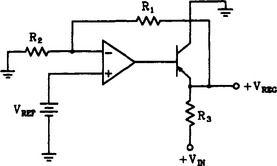
FIGURE 6.13 The error amplifier portion of the regulator circuit shown in Figure 6.12 is essentially a simple noninverting voltage amplifier.
The output voltage of the circuit, then, is computed by applying the basic gain equation.
In the case of the circuit shown in Figure 6.12, we can compute the regulated output voltage as
We estimate the current capability of the circuit by considering the case when +VIN is at its lowest level. Under these conditions, the maximum load current can be estimated with Ohm’s Law.
For the present case, we compute the highest allowable load current as
Although there can be a higher load current under higher input voltage conditions, the computed value of 86 milliamperes is the highest load current that we can supply under all input voltage conditions and still expect the circuit to remain in a regulated condition. Ohm’s Law can be used to determine the minimum value load resistor that can be used with the circuit. That is,
Transistor Q1 must be able to safely conduct the difference between the highest possible input current and the minimum possible load current. For many applications, we assume that the load can be disconnected and we therefore consider the minimum load current to be 0. If the regulator were an integral part of a system that made it impossible for the load to be disconnected (e.g., all part of the same printed circuit board), then the minimum load current could be greater than 0. For purposes of this analysis, we assume a worst-case situation, which means that Q1 must be able to handle a value of current given by Equation (6.15).
For the circuit shown in Figure 6.12, the maximum transistor current can be calculated as
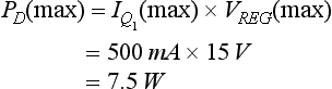
We can estimate the worst-case power dissipation in Q1 by applying our basic power formula.
For our present circuit, the transistor dissipation is estimated as
For many applications, the heat dissipated in the transistor will require a heat sink to keep the transistor within its safe operating range.
The shunt-regulator circuit is inherently current limited. That is, if we try to draw more current than it is designed to deliver, the output voltage will drop. Even if we short the output directly to ground, the current will be limited by resistor R3. If resistor R3 has a sufficiently high power rating, then the duration of the short can be any length. If it has a lower power rating, then the regulator is still short-circuit proof, but the duration of the overload must be less. If the output of the circuit in Figure 6.12 is shorted directly to ground, then the maximum current flow can be computed with Ohm’s Law as

The resulting power dissipation in R3 is computed with the basic power formula as
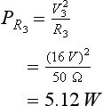
Since this clearly exceeds the 0.5-watt rating of the resistor as listed in Figure 6.12, we can expect the resistor to overheat and burn open. However, it can withstand momentary short circuits without having a higher power rating. A common way for momentary short circuits to occur is for your probe to slip off of a test point while troubleshooting a circuit.
6.3.3 Practical Design Techniques
Let us now design a shunt regulator circuit similar to the one shown in Figure 6.12. We will design it to meet the following design specifications:
| 1. Unregulated input voltage | +18 to +22 volts DC |
| 2. Regulated output voltage | +12 to +15 volts DC |
| 3. Load current | 0 to 150 milliamps |
| 4. Line regulation | <2 percent |
| 5. Load regulation | <2 percent |
| 6. Op amp | 741 |
Determine the Error Amp Voltage Gain.
Since the design calls for a variable output voltage, we will need to compute a range of error amp gains. As with the previous design, we will use the +4-volt reference circuit designed earlier in the chapter. The required voltage gains can be computed with Equations (6.8) and (6.9).

Let us plan to use a potentiometer between R1 and R2 of Figure 6.12 to adjust the gain of the error amp. This is similar to the method used with the series voltage regulator discussed in a prior section.
Select the Potentiometer.
Selection of P1 is not critical, and the guidelines discussed for the series regulator may be followed. That is, the minimum value for P1 should be at least 20 times the minimum equivalent load resistance. This is computed with Equation (6.10).
The maximum value is generally no more than a few tens of thousands of ohms. We will use a 10-kilohm potentiometer for P1 in this particular application.
Compute R2.
Equation (6.12) provides the tool necessary to compute the value for R2. We calculate it as follows:

For this application, we select the nearest standard value of 39 kilohms for R2.
Compute R1.
Resistor R1 can be calculated with Equation (6.11). For our present application, R1 is computed as shown:

Again, we use the nearest standard value of 100 kilohms because the application is not critical.
Determine the Value of R3.
Resistor R3 establishes the maximum possible load current from the shunt-regulator circuit. We can determine its value for a given application by applying Ohm’s Law at a time when the load current and output voltage are at maximum and the input voltage is at minimum. That is,
In our particular case, the required value for R3 is found as follows:
The power rating for R3 is determined by using the basic power formula under worst-case conditions:

Select Transistor Q1.
There are several transistor characteristics that must be considered when selecting a particular device for Q1:
The maximum collector current that the transistor will be expected to carry can be computed with Equation (6.15).

We estimate the highest current that should be supplied by the op amp as 25 percent of the short-circuit output current of the op amp. The short-circuit output current for a 741 is listed in the manufacturer’s data sheet as 20 milliamperes, so we will restrict the output current of the op amp to 25 percent of 20 milliamperes, or 5 milliamperes. We can now apply the basic current gain equation for transistors to determine the required transistor current gain.
This is a fairly high-current gain for a power transistor and may necessitate the use of a Darlington pair for Q1.
The power dissipation in Q1 can be found by applying Equation (6.16) under conditions of maximum output voltage.
This high-power dissipation is one major disadvantage of shunt-regulator circuits.
The collector-to-emitter breakdown voltage must be higher than VREG(max). In the present case, the transistor breakdown rating for VCEO must be greater than 15 volts.
Many transistors will satisfy the requirements of our design. For purposes of illustration, let us select an MJE2090, which, as the manufacturer’s data sheet (Appendix 2) indicates, is a Darlington power transistor that satisfies all of our requirements. The calculations presented in Appendix 10 dictate the use of a heat sink for the transistor.
The complete schematic of our shunt regulator circuit is shown in Figure 6.14. Its performance is demonstrated by the oscilloscope displays in Figure 6.15. Figures 6.15(a) and 6.15(b) show the effect of adjusting P1 between its limits. Figures 6.15(c) and 6.15(d) illustrate the circuit’s response to a change in load current from 0, in Figure 6.15(c), to 150 milliamperes, Figure 6.15(d). Finally, the original design goals are contrasted with the actual measured performance in Table 6.3.
TABLE 6.3
| Design Goal | Measured Value | |
| Input voltage | 18–22 volts | 18–22 volts |
| Output voltage | 12–15 volts | 12.5–15.5 volts |
| Output current | 0–150 milliamperes | 0–150 milliamperes |
| Line regulation | <2 percent | 0.8 percent |
| Load regulation | <2 percent | 0.012 percent |

FIGURE 6.14 A shunt regulator circuit designed to provide a variable output voltage and to supply a load current of 0 to 150 milliamperes


FIGURE 6.15 Oscilloscope displays showing the performance of the regulator circuit shown in Figure 6.14. (Test equipment courtesy of Hewlett-Packard Company.)
6.4 SWITCHING VOLTAGE REGULATORS
Our discussion on switching regulators will be limited to the theory of operation. Although a switching regulator can be designed around an op amp, most are built using specialized regulator ICs, which not only simplifies the design but generally improves the overall performance of the regulator circuit. Nevertheless, an understanding of the operation of switching regulators is very important to an engineer or technician working with equipment being designed today, and no discussion of regulated power supplies would be complete without this understanding.
6.4.1 Principles of Operation
Let us begin by examining the simplest of equivalent circuits. Figure 6.16 shows a simple switching circuit. Assume that the switch is operated at periodic intervals with equal open and closed times. When the switch is closed, the capacitor is charged by current flow through the coil. As current flows through the coil, a magnetic field builds out around it (i.e., energy is stored in the coil). When the switch is opened, the magnetic field around the coil begins to collapse, which makes the coil act as a power source (i.e., the stored energy is being returned to the circuit). You will recall from basic electronics theory that inductors tend to oppose changes in current. When the switch opens and the field begins to collapse, the resulting coil voltage causes circuit current to continue uninterrupted. The path for this electron current is right to left through the inductor, down through diode D, up through C (and the load) to the coil. This current will continue (although decaying) until the magnetic field around the coil has completely collapsed.
Now, if the switch were to close again before the coil current had time to decay significantly, and if it continued to open and close at a rapid rate, then there would be some average current through the coil. Similarly, this average current value would produce some average value of voltage across the capacitor and therefore across the parallel load resistor.
Suppose now that the ratio of closed time to open time on the switch is shortened. That is, the switch is left opened longer than it is closed. Can you see that the inductor’s field will collapse more completely, and that the average current through the coil (and therefore load voltage) will decrease? On the other hand, if we lengthen the closed time of the switch relative to the open time, the average load voltage will increase.
The basic behavior of capacitors is to oppose changes in voltage. That is, we cannot change the voltage across a capacitor instantaneously; the voltage can only change as fast as the capacitor can charge or discharge. The capacitor in Figure 6.16 is a filter and smooths the otherwise pulsating load voltage. So, even though the switch is interrupting the DC supply at regular intervals, the voltage is steady across the load because of the combined effects of the coil and capacitor. By varying the ratio of on time to off time (i.e., the duty cycle), we can vary the DC voltage across the load. If we sample the actual load voltage and use its value to control the duty cycle of the switch (a transistor in practice), then we will have constructed a switching regulator circuit.
Figure 6.17 shows a more accurate representation of a switching voltage regulator. Here the DC input voltage is provided by a standard transformer-coupled, bridge-rectifier circuit followed by a brute filter (C1). The interrupting device is an n-channel, power MOSFET (Q1). Gate drive for the MOSFET comes from a pulse width modulator circuit. This can be built around an op amp comparator/oscillator circuit, but is generally an integral part of an integrated circuit designed specifically for use in switching regulators.

FIGURE 6.17 A switching regulator controls the switching operation of the pass transistor to regulate load voltage.
The pulse width modulator has two inputs. One is the sample output voltage derived from a voltage divider (R1 and R2); the other is provided by a stable voltage reference. The pulse width modulator compares the reference voltage with the sampled output voltage (just as the series and shunt-linear regulators discussed in previous sections do) and alters the pulse width (effective duty cycle) of the signal going to the MOSFET. As the duty cycle of the MOSFET is altered, the average (i.e., DC) output voltage is adjusted and maintained at a constant value. If the load voltage tried to change, perhaps in response to a changing current demand, then this change would be fed back through the voltage divider to the pulse width modulator circuit. The pulse width going to the MOSFET would quickly be adjusted to bring the load voltage back to the correct value.
6.4.2 Switching versus Linear Voltage Regulators
Why go to all the trouble of interrupting the DC voltage and then turning right around and smoothing it back into DC again? Well, switching regulators do have some outstanding advantages over linear regulators. One of their primary advantages as compared to their linear equivalents is lower power dissipation.
In a linear regulator, the series pass transistor or the shunt regulator transistor dissipates a significant amount of power. Typical efficiencies for linear regulators are 30 to 40 percent, which means, for example, that a linear supply designed to deliver 12 volts at 3 amps DC actually draws at least 90 watts from the power line. The internal power loss results in heat, which in turn leads to cooling requirements like fans and heat sinks. Most of the power loss in a linear regulator is in the regulator transistors. Recall that their power dissipation is computed as
The switching regulator, on the other hand, typically achieves efficiencies on the order of 75 percent. This improvement is caused primarily by a dramatic reduction in power dissipation in the regulator transistor. Although the power dissipation is computed in the same basic way, the results are quite different because the transistor is operated in either saturation or cutoff at all times. Thus, although the power at any given time is expressed as
either IC is very low (at cutoff IC ≈ 0) or VCE is very low (during saturation VCE is ideally 0). Therefore, the only time the switching transistor dissipates significant power is during the actual switching time (a few microseconds).
The reduced power dissipation results in other advantages. Since the cooling requirement is less for a given output power, both size and cost of the associated circuitry and support components are less. It is reasonable to expect size reductions on the order of five or more.
Another advantage of switching regulators is that the output voltage can be stepped up, stepped down, and/or changed in polarity in the process of being regulated. This can simplify some designs.
Switching regulators are not without their disadvantages, however. First, they require more complex circuitry for control, although this is becoming less disadvantageous as more specialized regulator ICs are being provided to the power supply designer.
Another major disadvantage of switching regulators is electrical noise generation. Anytime a circuit changes states quickly, high-frequency signals are generated. You may recall from basic electronics theory that a square wave is made up of an infinite number of odd harmonics. So, if we have a 100-kilohertz square wave, we will be generating harmonic frequencies of 300 kilohertz, 500 kilohertz, 700 kilohertz, and so on. The Federal Communications Commission (FCC) in the United States and similar agencies in other countries restrict the amount of electromagnetic emissions that may leave an electronic device. For example, suppose you have designed a new computer that fits in the palm of your hand. The FCC will prevent you from marketing your new computer unless it can pass the FCC-defined emissions tests. Many new computer designs fail to pass these tests because of the electrical noise generated by switching power supplies. Now, this doesn’t mean you can never use a switching regulator in a computer. Quite the contrary, most computers do use switching regulators. But additional components will have to be included to filter the high-frequency noise that is generated. This noise can easily extend into the 450-kilohertz to 150-megahertz band.
Finally, although switching regulators are good, they cannot respond as quickly to sudden changes in line voltage or load current. That is, they do not regulate as well as their linear counterparts if the line and load changes are rapid.
6.4.3 Classes of Switching Regulators
We can categorize switching regulators into four general groups based on the method used to control the switching transistor:
1. Fixed off time, variable on time
2. Fixed on time, variable off time
First, it should be noted that all of the types listed work by switching the regulator transistor from full off to full on. Additionally, they all regulate by altering the ratio of on time to off time of the transistor. The various methods refer to the actual circuitry and waveform driving the switching transistor.
The first two regulator types listed are similar in that one alternation of the transistor drive signal is fixed. Regulation is achieved by adjusting the time for the remaining alternation. Because one alternation is fixed and one is variable, the frequency of operation inherently varies. These types are sometimes called variable frequency regulators.
The third class of switching regulators uses a constant frequency, but alters the duty cycle of the signal applied to the switching transistor. That is, if the on time is increased, the off time is decreased proportionately, so the output voltage can be controlled without altering the basic frequency of operation. This is one of the most common classes of switching regulators.
Finally, the burst regulator operates by gating a fixed-frequency, fixed-pulse width oscillator on and off. The duty cycle of the switching waveform is such that the output voltage would be too high if the switching were continuous. The circuit senses this excessive output voltage and interrupts or stops the switching completely. With the switching transistor turned off continuously, the output voltage will quickly decay. As soon as it decays to the correct voltage, the switching is resumed. Thus, the regulation is actually achieved by periodically interrupting the switching waveform going to the switching transistor.
6.5 OVER-CURRENT PROTECTION
Regulated power supplies are often designed to be short-circuit protected. That is, if the output of the supply is accidentally shorted to ground or tries to draw excessive current, the supply will not be damaged. There are several classes of over-current protection:
6.5.1 Load Interruption
The simplest form of over-current protection is shown in Figure 6.18. The protective device is generally a fuse (as shown in the figure), a fusible resistor, or a circuit breaker. In any case, once a certain value of current has been reached the protective device opens and completely isolates the load from the output of the supply. As long as the protective device is designed to operate at a lower current value than the absolute maximum safe current from the supply, the power supply will be protected from damage. Since the protective element has resistance, it can adversely affect the overall regulation of the circuit.

6.5.2 Constant Current Limiting
Figure 6.19 shows a common example of a constant-current limiting circuit. This is identical to the series regulators discussed earlier in the chapter with the addition of R1 and Q2, which are the current limiting components. Under ordinary conditions, the voltage drop across R1 is less than the turn-on voltage for the base-to-emitter junction of Q2 (about 0.6 volts). This means that Q2 is off and the circuit operates identically to the standard unprotected series regulator.

FIGURE 6.19 A constant-current limiting technique is often used to protect series regulator circuits from over-current conditions.
Now suppose the load current increases. This will cause an increased voltage drop across R1. As soon as the R1 voltage drop reaches the threshold of Q2’s base junction, transistor Q2 will start to conduct. The conduction of Q2 essentially bypasses the emitter-base junction of Q1, which prevents any further increase in current flow through Q1. We can better understand the operation of Q2 if we view it in terms of voltage drops. At the instant Q2 begins to turn on, there must be approximately 0.6 volts across R1 and another 0.6 to 0.7 volts across the emitter-base junction of Q1. Kirchhoff’s Voltage Law shows us that there must therefore be about 1.2 to 1.3 volts between the emitter and collector of Q2 when it starts to conduct, because the emitter-collector circuit of Q2 is in parallel with the voltage drops of R1 and the emitter-base circuit of Q1. Any further attempt to increase current beyond this point will cause a decrease in the emitter-collector voltage of Q2. As this voltage is in parallel with the series combination of Q1’s base-emitter junction and R1, these voltages also tend to decrease. However, if the base-emitter voltage of Q1 actually decreases, then the emitter current of Q1 decreases, causing the voltage drop across R1 to decrease, resulting in less conduction in Q2 (the opposite of what is really occurring). So, in essence, the current reaches a certain maximum limit and is then forced to remain constant. Any effort to increase the current beyond this point merely lowers the output voltage.
The value of current required to activate Q2 is determined with Ohm’s Law. We simply find the amount of current through R1 that it takes to get a 0.6-volt drop. That is, short-circuit current (ISC) is computed as follows:
6.5.3 Foldback Current Limiting
Figure 6.20 shows a simplified schematic diagram of a voltage regulator circuit that uses foldback current limiting. Note that resistors R4 and R5 have been added to the constant-current limiting circuit presented in Figure 6.19. Under normal conditions, transistor Q2 is off and the circuit works just like the unprotected regulator circuit discussed in an earlier section. Voltage divider action causes a voltage drop across R4, with the upper end being the most positive.

FIGURE 6.20 Foldback current limiting actually decreases the output current under overload conditions.
As load current increases, the voltage drop across R1 increases, as it did in the constant current circuit. However, the voltage across R1 must not only exceed the turn-on voltage of the base-emitter junction of Q2 in order to turn Q2 on, but also overcome the voltage across R4. Once this point occurs, however, Q2 begins to conduct and reduces the conduction of Q1. This, of course, causes both the output voltage and the base voltage of Q2 to decrease. However, because the base voltage of Q2 is obtained through a voltage divider, it decreases more slowly than the output voltage. And, because the emitter of Q2 is connected to the output voltage, it must also be decreasing faster than the base voltage. This causes Q2 to conduct even harder, further limiting the output current.
If the load current increases past a certain threshold, the circuit will “fold back“ the output current. That is, even if the output is shorted directly to ground, the current will be limited to a value that is less than the maximum normal operating current, which under overload conditions is a very desirable characteristic. Because the pass transistor will have the full input voltage across it when the output is shorted to ground, it is prone to high power dissipation. In fact, the constant-current limiting circuit previously discussed has maximum power dissipation under short-circuit conditions. By the current folding back under overload conditions, the dissipation of the pass transistor is reduced and a smaller device can be used.
6.6 OVER-VOLTAGE PROTECTION
Some applications require a regulator circuit with over-voltage protection to protect the load against regulator malfunctions. That is, under normal operating conditions, the output of the regulator should stay at the regulated level, but if the regulator fails (e.g., via emitter-to-collector short in the series pass transistor), the output may increase significantly over the regulated value and potentially cause damage to the load circuitry.
Figure 6.21 shows a common method of over-voltage protection that is built around a silicon-controlled rectifier (SCR). Under ordinary conditions, the voltage drop across R4 is less than the base-emitter turn-on voltage of Q2, and the circuit works identically to the unprotected circuit discussed earlier.

If a regulator malfunction causes the output voltage to rise above a threshold set by the ratio of R4 and R5, Q2 turns on and provides gate current for the SCR, which causes it to fire. When an SCR has fired and is in the forward conducting state, the voltage drop across it is about 1 volt. Thus, the base voltage of Q1 is quickly dropped to about 1 volt. Since the Q1 base voltage is 1 volt, the output voltage will be dropped to a few tenths of a volt, and this condition will continue as long as the SCR remains in conduction. To reset the SCR, the anode current must fall below a minimum value, called holding current. In the circuit shown in Figure 6.21, the main power source must be momentarily turned off to reset the SCR.
Capacitor C1 is a transient suppressor and prevents accidental firing of the SCR during initial turn-on of the regulator or as a result of a noise pulse.
Some power supply designs return the anode of the SCR directly to the unregulated DC input with no limiting resistance. If an over-voltage condition occurs and the SCR fires, the main supply is essentially shorted to ground via the SCR. This activates the current limiting features of the main supply (often a fuse in the primary of the supply transformer). When the SCR is connected in this way, the circuit is called a “crowbar” because it essentially throws a short circuit (like a steel crowbar) directly across the power supply.
6.7 POWER-FAIL SENSING
An op amp can be configured as a voltage comparator circuit and used to sense an impending power failure. This is commonly used in computer systems to protect the computer from erratic operation caused by power loss. If an impending power failure is detected, the computer quickly transfers all of the critical data to a permanent storage area that does not require power. Once power has been restored, the computer retrieves the stored data from the permanent memory and resumes normal operation. Figure 6.22 shows how an op amp can be used to detect an impending power failure and send a signal to a computer in time to save the critical data before the power actually goes away.

Under normal conditions, the inverting (−) input of the voltage comparator is more positive than the noninverting input. This is true even under conditions of minimum unregulated voltage. If a primary power loss occurs, the unregulated DC voltage will, of course, drop to 0; however, the filter capacitors (usually quite large) in the power supply will prevent the unregulated DC supply from decaying instantaneously. The regulator will continue to supply a constant voltage until the unregulated input voltage has decayed past a certain minimum point. Thus, up to a point, the voltage on the (−) input to the comparator decays while the voltage on the (+) input remains constant. When the voltage on the (−) input passes the lower threshold of the voltage comparator, the output quickly changes states, signaling a coming power loss. A computer monitoring this signal can then take the necessary action to protect critical data. Resistors R3 and R4 provide hysteresis for the comparator.
The amount of time between primary power interruption and the point where the regulated output begins to drop is called hold-up time and is generally tens or even hundreds of milliseconds. Since a computer executes in the microsecond range, there is plenty of time to save the critical information after the unregulated input has started to decay but before the regulated output begins to drop.
6.8 TROUBLESHOOTING TIPS FOR POWER SUPPLY CIRCUITS
Power supply circuits are considered by some technicians and engineers to be simple, fundamental, nonglamorous, and even boring. However fundamental or boring the purpose of power supplies may be, the troubleshooting of a defective supply is not always a simple task. What complicates the troubleshooting of a regulator circuit is the closed-loop nature of the system. A defect in any part of the loop can upset the voltages at all other points in it, thus making it difficult to distinguish between cause and effect.
Nevertheless, armed with a thorough understanding of circuit operation and guided by systematic troubleshooting procedures, a defective regulator circuit can be quickly and effectively diagnosed. The following sequential steps will provide the basis for a logical, systematic troubleshooting procedure applicable to voltage regulator circuits:
1. Observe the symptoms. Because of the potentially high-power levels available in a supply, visible signs of damage are common. DO NOT, however, simply replace a burned component and reapply power—in many cases, the burned component is the result of a malfunction elsewhere in the supply. Nevertheless, detecting the burned component will help you narrow the range of possibilities.
Symptom observation also includes taking careful note of the output symptoms. Is the output voltage too high, too low, 0, unregulated? Did the user of the equipment say how the problem was caused (e.g., an accidental short on the output)?
2. Verify that the input to the regulator is correct. If it is not correct, the regulator may not be the cause. On the other hand, if the problem is no input and the unregulated supply shows signs of damage, then suspect a short in the regulator circuit. In these cases, it is often helpful to disconnect the regulator circuit and get the unregulated supply back to normal as a first step. A simple way to disconnect series regulator circuits is to remove the pass transistor. This is a particularly simple task for socket-mounted power transistors.
3. Check for possible short circuits. Once the unregulated input voltage is shown to be correct, we can concentrate on the regulator portion of the supply. If the regulator was disconnected during step 2 and you have reason to believe a short circuit exists in the regulator, DO NOT reconnect the regulator and apply full power. If you do and a short does exist, the newly repaired unregulated source will be damaged again. A better approach is to connect the regulator to the unregulated supply via a current meter. Use a variable autotransformer to supply the AC power to the unregulated power supply, and slowly increase the AC input voltage while monitoring the current meter. If a short exists in the regulator, the current meter will exceed normal values with a very low-input voltage. If this is the case, you must rely on your theory of operation and an ohmmeter as your major tools.
4. Open the regulator loop. If the full supply voltage can be applied safely, but the regulator still doesn’t work properly, then you can add a voltmeter to your tool kit. Since the regulator is inherently a closed-loop system, it is often difficult to distinguish between cause and effect. If the loop can be easily broken (e.g., removing a wire from the wiper arm of a potentiometer, removing a socket-mounted transistor, etc.), this can help isolate the problem. After the loop has been opened, you can inject your own “good” voltage at the open-loop point from an external DC supply. The system can then be diagnosed using the split-half method, signal tracing, and so on, like any other open-loop system.
5. Force the circuit to known extremes. If it is impractical to open the loop of the regulator, you can sometimes force a condition at one point in the loop and watch for a response at another point. Your understanding of the operation of the components between the forced point and the monitored point can lead you to the problem. A good example of forcing a condition is to either short the emitter-base circuit of a transistor to force it to cut off, or to short the emitter-collector circuit to simulate a saturated condition. Be sure to examine the circuit carefully before shorting these elements, but in most circuits neither of these shorts will cause damage (see step 6), although they will force the circuit to go to one of two extremes. The extreme change will be passed through the rest of the circuit if everything is normal. A defect, however, will not respond to the change and thus reveal its identity to an alert technician or engineer.
6. Use special care with switching regulators. Here the regulator transistor has been selected on the assumption that it is switching from full on to full off and therefore dissipating minimum power. If any portion of the regulator circuit causes the switching to stop and the pass transistor is in the ON state, then the pass transistor will almost certainly be damaged. This has two important ramifications. First, if your diagnosis reveals that no switching signal is being applied to the switching transistor, then suspect a bad transistor after you correct the switching signal problem. Second, you should never intentionally stop the oscillation in a switching supply by shorting components as described in step 5.
7. Substitute the load. Another method that can be helpful in isolating some power supply defects is to remove the load. This eliminates the possibility that a malfunction in the system is causing the supply to appear defective. If the supply is shown to be defective, substituting an equivalent resistance in place of the system circuitry can simplify troubleshooting of the actual power supply. Additionally, it removes the possibility of causing damage to the system circuitry if the output of the supply becomes excessively high while troubleshooting the problem. (For example, a test probe may slip and cause a momentary short circuit.)
REVIEW QUESTIONS
1. List the three basic classes of voltage regulator circuits.
2. If the DC output voltage of a shunt regulator circuit varies between 11 and 12.5 volts as the input line voltage varies from 110 to 130 volts, what is the percent of line regulation for the regulator?
3. If a series regulator circuit provides 25 volts DC under no-load conditions, but drops to 24.3 volts when a full load is applied, what is the percent of load regulation for the regulator circuit?
4. If each of the following rectifier/regulator circuits requires 1.2 amps of current from the 120-VAC input line, which one will probably deliver the highest current to a 12-VDC load: series, shunt, switching? Explain your choice.
5. Refer to Figure 6.8. If the input voltage is 16.8 VDC and the regulated output voltage is 8.9 volts DC, what is the power dissipation of Q1 with a 300-mA load connected?
6. Refer to Figure 6.8. If the reference voltage has a defect that causes it to go to +6 volts, what is the effect on output voltage (increase, decrease, remains the same)? Explain your answer.
7. Refer to Figure 6.8. If resistor R2 increases in value, what relative effect does this have on output voltage?
8. Refer to Figure 6.9. What is the effect on output voltage if resistor R2′ increases in value?
9. Refer to Figure 6.12. What is the effect on the current flow through Q1 if resistor R2 is decreased in value? Explain your answer.
10. If resistor R3 in Figure 6.12 is changed to 40 ohms (and no components are damaged), what will happen to the value of reference voltage? What will happen to the value of output voltage (+VREG)? What will happen to the value of current through Q1? Will the current through R1 change?
11. Refer to Figure 6.19. What is the effect on the current flow through the load resistor (assume a constant value of load resistance) if resistor R2 is increased in value?
12. Refer to Figure 6.19. What happens to the value of voltage dropped across the emitter-collector circuit of Q1 if resistor R3 is increased in value?
13. Refer to Figure 6.20. What is the effect on circuit operation if transistor Q2 develops an emitter-to-collector short?
14. Refer to Figure 6.21. What is the effect on circuit operation if capacitor C1 develops a short circuit?
15. Refer to Figure 6.21. What is the effect on circuit operation if resistor R4 becomes open?