
Digital-to-Analog and Analog-to-Digital Conversion
The world of electronics can be neatly divided into two general classes based on the nature of the signal or circuit: digital and analog. Digital signals, devices, and circuits operate in one of two states at all times. These states may be high/low, on/off, up/down, 0 volts/5 volts, −5 milliamps/+5 milliamps, or any other set of two-valued terms.
Analog signals, devices, and circuits, on the other hand, operate on a continuous range with an infinite number of values represented within a given range. An analog voltage, for example, may be 1.5 volts or 1.6 volts, but it can also be an infinite number of values between these two numbers, such as 1.55 volts or 1.590754 volts.
A technician or engineer generally must be capable of working with both analog and digital devices and systems. This text will avoid revealing a prejudice toward one type or another, and the reader is encouraged to avoid developing such a prejudice. It is true that digital devices and techniques are steadily taking over operations and functions previously implemented by analog systems. But equally true is the fact that the world in which we live is inherently analog. Temperature, pressure, weight, speed, light intensity and color, volume, and all other similar quantities are analog in that they vary continuously and have an infinite number of possible values.
This chapter will focus on the circuits that interface analog with digital systems. Analog-to-digital (A/D) converters accept an analog signal at their input and produce a corresponding digital signal at the output. This output can then be processed and interpreted by a digital circuit (typically a microprocessor system). A digital-to-analog (D/A) converter, on the other hand, is used to convert the digital output from a microprocessor or other digital device into an equivalent analog signal. The analog signal is frequently used to control a real-world quantity (e.g., temperature or pressure).
The intent of this chapter, then, is to provide the reader with the concepts and terminology associated with A/D and D/A conversion. Additionally, several representative circuits will be presented that utilize operational amplifiers. An understanding of the operation of these fundamental circuits is important because they convey essential underlying principles. The actual implementation of the converter circuits, however, is another matter. Except for unique or very demanding applications (neither of which is targeted by this text), most A/D and D/A converter applications are resolved by an integrated circuit version of the A/D or D/A converter. The price and performance of these circuits makes them very difficult to beat by designing your own.
8.1 D/A AND A/D CONVERSION FUNDAMENTALS
The concepts and terminology presented in this chapter are important to the reader whether designing a custom converter circuit or selecting an integrated version. In either case, the technician or engineer must be able to effectively evaluate the application and contrast it with the specifications of the converter circuit.
8.1.1 Analog-to-Digital Converters
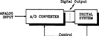
Figure 8.1 illustrates the fundamental function of A/D conversion. The block labeled “A/D Converter” may be an integrated circuit or an array of op amps and other devices. In any case, it accepts the analog signal as its input and produces a corresponding digital output. The digital output is shown to consist of several lines, the number of which varies with the resolution of the converter. Resolution describes the percentage of input voltage change required to cause a step change in the output. Table 8.1 shows the basic relationship between number of bits (lines) and equivalent resolution.
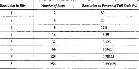
Suppose, for example, an 8-bit A/D converter was designed to accept 0-volt to 10-volt input signals. The 10-volt range would be divided into 256 discrete steps of 10/256, or about 39 millivolts per step. By contrast, a 4-bit A/D converter would have less resolution, with each of the 16 output steps being equivalent to 6.25 percent of the full-scale input, or 625 millivolts. Thus, the higher the resolution (i.e., the number of bits in the converted output), the smaller the input change required to move to the next output step. Typical applications require resolutions of 8, 12, or 20 bits.
Since the analog input may take on any one of an infinite number of values but the output must be resolved into a fixed number of discrete levels or steps, each output step inherently represents a range of input voltages. The process of forming discrete groups from the continuous input is called quantization, so the output does not exactly represent a given input value; rather, it represents an approximation. The resulting error is called quantization uncertainty and is equal to ±1/2 the value of the least significant bit of the converted output. In the example of the 8-bit converter described, this equates to an uncertainty of ±1/2 × 39 millivolts, or about ±19.5 millivolts. The magnitude of the quantization uncertainty is less with greater resolution. Therefore, if we need less quantization error, we must increase the number of bits in the output.
When the input signal is converted to a digital output, we normally expect that steadily increasing values of input will produce equally spaced digital values in the output. Sometimes, however, the output may skip one or more steps or digital numbers. Similarly, the output may remain on a given step throughout a range that ideally includes two or more steps. This type of performance is generally caused by linearity errors. If the converter has no linearity problems, then the amount of input change to produce a change in the output will be consistent throughout the entire range of operation. When the amount of input change needed to reach the next step in the output varies, we call this variation nonlinearity.
Another characteristic of A/D converters describes the polarity of output changes when a steadily increasing input is applied. With an increasing input signal, we expect (and want) a series of digital numbers in the output that are progressively larger. It is possible, however, for a particular output step to be smaller than the preceding step. That is, the magnitude of the digital output decreases rather than increases on a particular step. This type of output response is called nonmonotonic. That is, a converter whose output is progressively higher for progressively higher inputs has the property of monotonicity.
Sometimes the intended range of input signals does not match the actual range. For example, the converter may be designed to accept a 0-volt to 10-volt input, but the actual device may be found to produce a maximum digital output for a 9.7-volt input. This discrepancy in full-scale operation is called gain error or scaling error.
The entire operational range of the A/D converter can be shifted up or down. For example, it may be designed to produce a minimum digital output with 0 volts on the input; however, actual measurement may reveal that a DC offset voltage must be applied at the input in order to produce the minimum digital output. This is called the offset error and is often expressed as a percentage of full-scale input voltage.
Accuracy is a term used to describe the overall performance of an A/D converter. It includes the combined effects of all errors and measures the worst-case deviation from a given input signal and the equivalent value of its converted digital output.
The amount of time required to generate a particular digital number to represent a given analog input signal is called conversion time. Alternately, the number of these conversions that can be accomplished in one second is called conversion rate.
8.1.2 Preamplifiers
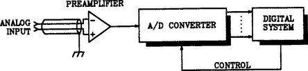
Many A/D converter applications involve the conversion of transducer signals into corresponding digital numbers for subsequent processing by a microprocessor or programmable logic controller (PLC). Transducer signals are frequently very low level (current or voltage) and require amplification before they can be effectively applied to an A/D converter. Operational amplifiers are often used for this purpose, as are special differential amplifiers called instrumentation amplifiers. Instrumentation amplifiers offer a very high rejection to common-mode signals (e.g., 60 Hz hum picked up on long cables), but offer high amplification to differential-mode signals (e.g., the actual transducer signal). These devices are discussed in greater detail in Chapter 11. Figure 8.2 shows the position of the preamplifier with respect to the A/D converter.
8.1.3 Sample-and-Hold Circuits
As mentioned previously, the conversion of an analog signal into an equivalent digital number requires a certain amount of time (conversion time). Since the analog signal may be changing values during the conversion process, substantial errors may be introduced. To eliminate this problem, we introduce a sample-and-hold (S/H) circuit between the preamplifier and the A/D converter. Figure 8.3 shows a block diagram for this case.
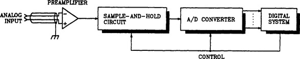
FIGURE 8.3 A sample-and-hold circuit is used to provide a steady input for the A/D conversion circuit.
An S/H circuit is similar to the peak detector circuit presented in Chapter 7, but it is gated on and off. When the S/H circuit receives the track command, it follows (i.e., samples) the input voltage. When a hold command is received, the S/H circuit opens its link to the input signal and holds the most recently sampled value at its output. This output is held constant throughout the conversion time of the A/D converter. Once the conversion has been completed, the track command is issued and the cycle repeats.
Once the track command has been received by the S/H circuit, it takes a certain amount of time for the output to match the present level of analog input. This delay is called the acquisition time. Similarly, there is a delay between the issuance of a hold command and the actual disconnecting of the S/H circuit from the input signal. This delay is called the aperture time.
The sampled input voltage is held constant by utilizing the charge on a capacitor. Although the capacitor has a very low discharge current, it does eventually leak off, causing the S/H output to slowly decay or decrease. The rate at which this occurs is called the droop rate.
The more often a signal is sampled, the better the digital representation of the analog signal. If the input signal changes rapidly relative to the speed of the conversion process, then substantial portions of the input signal will be missed (i.e., will go undetected). As an absolute minimum, the input signal must be sampled twice during each cycle. That is, the sampling rate must be at least twice the highest frequency component present in the input signal. While this may sound like a serious limitation, the use of a sample-and-hold circuit actually extends the highest usable frequency of an A/D converter by several thousand times.
Sample-and-hold circuits are available in integrated form. The AD386 is a sample-and-hold amplifier manufactured by Analog Devices, Inc., that offers a 3.6-microsecond acquisition time, a 12-nanosecond aperture time, and a 20-millivolt-per-second droop rate.
8.1.4 Multiplexers
Many systems have several analog inputs that are monitored by a single computer or digital system. Each of these signals must be converted before the computer can process the signal. Since the A/D conversion circuitry can be quite expensive (relative to other subsystems), many designers opt to multiplex several analog inputs through a single A/D converter circuit. This technique is illustrated in Figure 8.4.

FIGURE 8.4 A multiplexer is used to route several analog inputs through a single A/D conversion circuit.
The multiplexer acts like a rotary switch that connects each of the analog inputs to the S/H circuit on a one-at-a-time basis. The position and timing of the “switch” are controlled by the computer or digital system. There should be total isolation between the channels of a multiplexer circuit, but sometimes signal voltages from one channel will couple into another channel (generally via stray or internal capacitance). The resulting interference is called crosstalk.
This approach to system design can make it possible to use higher-performance (i.e., more expensive) sample-and-hold and A/D converter circuits by requiring only one such circuit for multiple inputs.
Multiplexers are available as integrated circuits. The AD7506 manufactured by Analog Devices, Inc., is a 16-channel device designed to select 1 of 16 analog input signals and connect it through to a single analog output.
8.1.5 Digital-to-Analog Converters
Figure 8.5 shows the basic configuration for digital-to-analog (D/A) conversion. The digital system (frequently a microprocessor) computes the required value of analog signal and outputs an equivalent digital number. The D/A converter circuit then converts this digital number into an analog voltage or current for use by the external analog device.
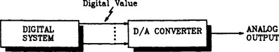
FIGURE 8.5 A digital-to-analog converter is used to make a digital signal (number) compatible with an analog system.
Since the input to the D/A converter has a finite number of digital combinations, the resulting analog output also has a limited number of possible values (unlike pure analog signals, which may have an infinite number of values). The greater the number of possible values, the closer the analog output will be to the ideal value. The number of possible levels is determined by the number of lines or bits in the digital number. More specifically, the number of states is computed as 2N where N is the number of bits in the digital number. For example, an 8-bit D/A converter could be expected to produce 28, or 256, discrete output steps. If the full-scale range of the converter is 0 to 10 volts, then each step will be 10/256, or about 39 millivolts. If finer resolution is required, we need more bits in the digital number. Thus, a converter with 10-bit resolution would provide 210, or 1024, steps with each step being equivalent to 10/1024, or about 9.8 millivolts.
Accuracy of a D/A converter describes the amount of error between the actual output of the converter and the theoretical output for a given input number. This rating inherently includes several other sources of error.
A certain amount of time is required for the output of a D/A converter to be correct once a particular digital number has been applied at the input. Two major factors cause this delay. First, it takes time for the changes to pass through the converter circuitry; this is called propagation time. Second, the output of the D/A converter has a maximum rate of change called slew rate, which is identical to the slew rate problems discussed with reference to op amps. The delays caused by slew rate limiting and propagation time are collectively referred to as settling time—the total time required for the analog output to stabilize after a new digital number has been applied to the input.
The overall operating range of a D/A converter can be shifted up or down from the optimum point. This DC offset is called offset error. In a somewhat similar manner, one end of the range can be correct but the other extreme too high or too low. This is called a gain error or scaling error.
As with A/D converters, we normally want a monotonic output. In other words, the output should increase whenever the input number increases. However, it is possible for a D/A converter to have a reduction in analog output at a particular point in its range, even though the digital input is increasing uniformly.
Figure 8.6 shows the performance of a low-quality D/A converter. Several of the potential problems described are present in the converted waveform. The input to the converter is a 4-bit down counter (e.g., 15, 14, 13 … 2, 1, 0, 15), and the analog output should be 16 equally spaced, decreasing steps for each cycle, producing a reverse sawtooth waveform. If you examine the waveform carefully, you can see the 16 distinct output levels; however, the steps are not equal in amplitude (linearity problems)—the midpoint level actually increases instead of decreases (nonmonotonic), and there are several glitches caused by switching transients. Although the performance indicated by the waveform in Figure 8.6 is certainly not representative of a practical D/A converter, it does provide an excellent example of several terms and definitions.
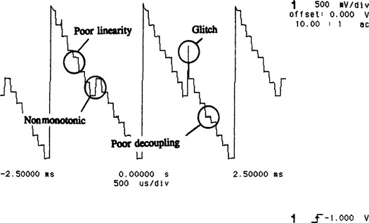
FIGURE 8.6 Oscilloscope display showing several imperfections in a low-quality D/A converter. (Test equipment courtesy of Hewlett-Packard Company.)
Let us now examine the actual circuitry for several of the more common methods of D/A and A/D conversion.
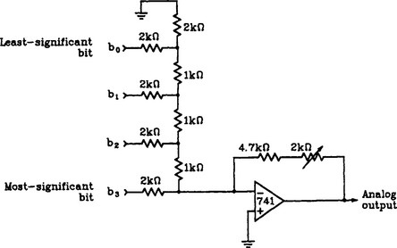
8.2 WEIGHTED D/A CONVERTER
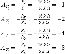
Figure 8.7 shows the schematic diagram of a weighted digital-to-analog converter circuit built around a 741 op amp. You should recognize the configuration as being identical to the inverting summing amplifier discussed in Chapter 2. Recall that the gain for each input is determined by the ratio of the feedback resistor and the respective input resistor. In the circuit in Figure 8.7, the individual gains are as follows:

For purposes of analysis, let us suppose that the two levels for the digital input signals are 0 and −1 volt. Table 8.2 shows the correlation between the digital number and the state of the four inputs.
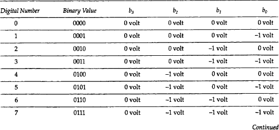

You will likely recall from the discussion of inverting summing amplifiers that the output voltage, at any given time, can be determined simply by adding the output voltages computed for each input individually. For example, if a digital number 5 were input to the circuit, the output voltage would be computed as follows:

The scaling factor for the converter is such that each step in the output corresponds to 1 volt, which means that the analog voltage output will be the same numerical value as the digital input. This is not necessarily true for all converters—the full-scale digital input for a 4-bit converter will always be 1111 (decimal 15). The full-scale output for the D/A converter shown in Figure 8.7 is 15 volts, but it could just as easily be 5 volts, 10 volts, or any other number depending upon the scale factor of the converter circuit.
For satisfactory performance, the input resistors must be very carefully selected (i.e., precision values) in order to maintain the correct ratios. If one or more resistors are the wrong value, the output will exhibit problems that include poor linearity and/or lack of monotonicity. Even with careful selection of resistors, the simple weighted D/A converter is only useful for small numbers of bits, since the ratio of the smallest to the largest resistor quickly becomes impractical—that is, the ratio increases as 2N−1, where N is the number of bits in the input. For example, the resistor in the least significant input of a 10-bit converter would be 210−1, or 512 times larger than the resistor for the most significant input.
A variation of the basic weighted D/A converter involves dividing the bits into two or more groups and converting each group separately. The weighting resistors for each group are identical, and the outputs from each of the individual converters can then be summed into a weighted, summing amplifier to produce the final output.
8.3 R2R LADDER D/A CONVERTER
One of the most popular methods for D/A conversion is shown in Figure 8.8. It is called an R2R ladder D/A converter, since the input network resembles the rungs on a ladder and the resistors in the input network are either equal (R) or have a 2:1 ratio (2R). One advantage of the R2R converter over the weighted converter previously discussed is immediately apparent; the resistors have a 2:1 ratio regardless of the number of bits being converted. This makes matching resistors much easier and even makes the use of integrated resistors practical.
An easy way to analyze the operation of the circuit is to Thevenize the input circuit for one or more digital input numbers. This process was described in Chapter 1. Once the input circuit has been simplified with Thevenin’s Theorem, you will be left with a simple inverting amplifier circuit whose input voltage is the Thevenin equivalent voltage and whose gain is determined by the ratio of feedback resistance to Thevenin equivalent input resistance. By performing several analyses with different input numbers, you will discover that the least significant input (b0) produces the least effect on output voltage, and the next input (b1) has twice as much effect on output voltage. Similarly, bit b2 has twice the effect of b1 but only half the effect on output voltage of b3. These variable effects are identical to the relative weights of the digits in a binary number.
The actual performance of an inexpensive R2R ladder D/A converter circuit similar to the one shown in Figure 8.8 is revealed by the oscilloscope waveform in Figure 8.9. Although the linearity is certainly less than optimum, it clearly illustrates the principles involved and would be adequate for many D/A applications. The linearity could be greatly improved by using precision resistors (rather than 5 percent) and by driving the digital inputs via analog switches (rather than directly from the output of a digital counter). Figure 8.9(a) shows the actual output of the converter, with the 16 distinct output levels in the waveform easily seen. Figure 8.9(b) shows the same basic circuit after the output has gone through a simple low-pass filter. The abrupt changes in the output are now gone, leaving us with a cleaner analog signal.

FIGURE 8.9 Oscilloscope displays showing the performance of the 4-bit D/A converter shown in Figure 8.8. (Test equipment courtesy of Hewlett-Packard Company.)
For noncritical applications, construction of your own D/A converters is feasible. However, the low cost and high performance (e.g., laser-trimmed ladder resistors) available in integrated converters makes these devices the best choice for many applications. An example of such a device is the TDC1016 10-bit D/A converter manufactured by Raytheon Semiconductor.
8.4 PARALLEL A/D CONVERTER
Parallel A/D conversion (sometimes called flash conversion) is the fastest technique available and the simplest to understand. However, its practicality is limited to small numbers of bits, since it requires 2N – 1 comparator circuits in order to produce an N-bit digital output. For example, producing a 3-bit digital output (8 states) requires 23 – 1, or 7, comparator circuits plus a significant amount of logic circuitry. Figure 8.10 shows the complete schematic diagram of a 3-bit parallel A/D converter circuit (including decoder logic).

The operation of the circuit is very straightforward. The voltage divider provides a stable reference for one input of each of the seven voltage comparators. Further, each voltage tap on the divider is 1.25 volts higher than the preceding one, which effectively divides the 10-volt range into 8 distinct ranges. These ranges and the corresponding comparator outputs are shown in Table 8.3, which also shows the converted digital output for each voltage range.
TABLE 8.3
| Voltage Range | Comparator States | Digital Result |
| 0 ≤ vIN < 1.25 Volts | 0000000 | 000 |
| 1.25 Volts ≤ vIN < 2.5 Volts | 0000001 | 001 |
| 2.5 Volts ≤ vIN < 3.75 Volts | 0000011 | 010 |
| 3.75 Volts ≤ vIN < 5 Volts | 0000111 | 011 |
| 5 Volts ≤ vIN < 6.25 Volts | 0001111 | 100 |
| 6.25 Volts ≤ vIN < 7.5 Volts | 0011111 | 101 |
| 7.5 Volts ≤ vIN < 8.75 Volts | 0111111 | 110 |
| 8.75 Volts ≤ vIN < 10 Volts | 1111111 | 111 |
The converted digital output for the given converter is in standard binary format. Actual converter circuits, however, may use any one of a variety of codes, including binary, Gray Code, excess-3, and others.
It is also possible to utilize the parallel converter in a hybrid configuration that gains some of the advantage of parallel conversion and yet avoids the geometrically increasing complexity normally associated with it. This hybrid method essentially consists of applying the analog voltage to a small (4–7 bits) parallel converter. This converter generates the most significant bits in the converted number, and the digits are then reconverted to analog with a D/A converter and subtracted from the original input signal. The difference voltage is then converted with a second parallel converter to produce the least significant bits of the digital result. This multistage method of parallel A/D conversion is faster than nonparallel methods but slower than a pure parallel approach. The complexity, however, is less than that of a pure parallel converter circuit. The AD9028 high-speed 8-bit A/D converter circuit, manufactured by Analog Devices, Inc., is an example of a parallel converter. It can deliver an 8-bit output in 3.3 nanoseconds.
8.5 TRACKING A/D CONVERTER
Figure 8.11 shows the schematic diagram of a tracking A/D converter. Here, the op amp plays a small but important role as a voltage comparator.

FIGURE 8.11 A tracking A/D converter will continuously follow (i.e., track) the analog input signal.
To understand the operation of the circuit, let us begin by assuming that the counter is at 0 and the analog input is at some positive voltage. The output of the counter (0 at the present time) is converted to an analog voltage by a D/A converter and applied to one input of a comparator. The other input is the amplified analog input signal. Under the given conditions, the output of the comparator will be low. The control unit interprets this comparator output to mean that the counter output is lower than the analog input, so the counter is allowed to increment.
This situation continues on each subsequent clock pulse until the counter has incremented to a value that exceeds the analog input voltage. When this point is reached, the output of the D/A will be higher than the analog input voltage, causing the comparator output to go to a high level. The control unit interprets this to mean that the counter has exceeded the input and directs the counter to begin counting down.
As the counter decrements, the output of the D/A becomes less. As soon as the D/A output falls below the analog input, the output of the comparator switches low again and causes the counter to start incrementing once more. Thus, as the input changes the counter automatically tracks it.
Every time the comparator changes state, the control unit transfers the counter value to a latch where it is accessible to other circuitry. This method is simple and inexpensive, but it is not particularly fast (especially for large input changes). For example, let us assume that the clock is operating at 20 megahertz and the converter is designed to provide a 16-bit output. If the input signal makes a small (equivalent of 1 bit) change, then it will take the circuit 1/20 megahertz, or 50 nanoseconds, to provide a valid output. However, if the input makes a full-range step change, it takes the converter (1/20 MHz) × 216, or 3.28 milliseconds, to provide a valid result. This converter is best suited for either slow signals or signals that make only small changes at any given time.
The oscilloscope display in Figure 8.12 shows the performance of an actual tracking A/D converter circuit. The two superimposed waveforms are taken from the two inputs of the op amp voltage comparator (refer to Figure 8.11). Near the left side of the screen, the analog input signal makes a large step change. It takes the counter and A/D circuit six clock pulses to climb to the new input level. At this point, the counter and A/D signal oscillate back and forth on either side of the analog signal. This oscillation in the least significant bit will always occur, since the counter must always count either up or down.
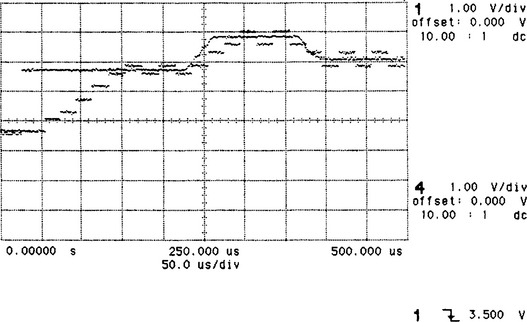
FIGURE 8.12 Oscilloscope display showing the operation of a tracking A/D converter circuit. (Test equipment courtesy of Hewlett-Packard Company.)
Near the center of the screen in Figure 8.12, the analog input makes another upward change, which the counter and D/A output can be seen to track. Similarly, when the input makes a negative transition, the counter and D/A output continue to track the input signal. The response time of the tracking A/D converter is determined solely by the frequency of the input clock.
8.6 DUAL-SLOPE A/D CONVERSION
Figure 8.13 shows the schematic diagram of a basic dual-slope A/D converter. Let us first examine each of its subcircuits and then analyze the overall operation of the circuit.

The heart of the circuit is an op amp, linear ramp generator circuit. Figure 8.14 shows the ramp generator isolated from the rest of the converter circuit. It is designed such that the charging current for capacitor C will always be constant. Basic circuit theory tells us that a constant charging current through a capacitor produces a linear ramp of voltage.

FIGURE 8.14 The linear ramp generator portion of the circuit shown in Figure 8.13.
To understand the operation of the ramp generator circuit, let us assume that the capacitor is initially discharged (i.e., 0 volts). This is the purpose of transistor Q1—as long as it is saturated, capacitor C cannot accumulate a charge. Although the actual saturation voltage of Q1 may be a few millivolts, let us assume it is truly 0 volts for simplicity. Let us further assume (as an example) that the input voltage to the ramp generator is +5 volts. Now let us cut off transistor Q1 and allow capacitor C to begin charging. We will compute the current through the capacitor at several times.
At the first instant after Q1 is cut off, the capacitor has 0 volts of charge. Ohm’s Law tells us that resistor R1 will have a current of
The op amp is essentially a noninverting amplifier with respect to the capacitor voltage. The voltage gain is given by our basic equation for noninverting amplifiers.
The output voltage at this instant will be 0 volts (i.e, 0 × 2). Resistor R2 will have 0 volts on both ends, which means it has no current flow through it. We know that negligible current flows in or out of the (+) terminal of the op amp. Now, since 2.5 milliamperes of current is flowing through R1, but no current flows to the op amp or through R2, we can apply Kirchhoff’s Current Law to conclude that the entire 2.5 milliamperes must be flowing into capacitor C as a charging current. The direction of the electron current is from ground, up through capacitor C, and through R1 to the positive 5-volt source. This establishes the initial slope of the charge on C. If we can maintain a constant current, we will maintain a linear slope across C.
Now let us examine the circuit condition after capacitor C has accumulated 1 volt of charge (positive on top). The current through R1 can now be computed as
With 1 volt on the capacitor and a voltage gain of 2, we can compute the output voltage of the op amp as
The current through R2 can be found with Ohm’s Law, since it has 1 volt on the left end and 2 volts on the right end.
Again, Kirchhoff’s Current Law will let us conclude that if 2 milliamperes are flowing to the left through R1 and 0.5 milliampere is flowing to the right through R2, then capacitor C must still be charging with a 2.5-milliampere current. Let us examine the circuit at one more point.
Suppose we let capacitor C accumulate a charge of 4 volts. The current through R1 will then be
With +4 volts on the capacitor, the output voltage of the op amp must be
The current through R2 can be calculated as
Finally, we apply Kirchhoff’s Current Law to show that with 0.5 milliampere flowing right to left through R1 and 2 milliamperes flowing left to right through R2, there must surely be 2.5 milliamperes flowing upward through capacitor C. Since the current through capacitor C has remained constant at 2.5 milliamperes, we know that the voltage across it will be a linearly rising ramp. The slope of the ramp is given by the basic capacitor charge equation:
For the present case, the slope of the ramp across C is computed as
The output of the op amp will have a slope that is linear but twice as great, since the amplifier has a voltage gain of 2. In either case, the slope of the ramp is determined by the charging current of C, which is determined by the value of input voltage.
Now, let us analyze the overall operation of the dual-ramp A/D converter shown in Figure 8.13. The input voltage to the ramp is switch-selected as either the analog voltage to be converted (positive) or a fixed, negative reference voltage. Recall that the input voltage to the ramp circuit determines the slope of the ramp. The position of the analog switch is controlled by the state of the most significant bit (MSB) of a counter. More specifically, if the MSB is low, then the switch will connect the analog input to the ramp generator. If the MSB of the counter is high, then the switch connects the negative reference voltage to the ramp generator input.
The counter is enabled (i.e., allowed to count) as long as the output of the ramp generator is positive. That is, as long as the ramp is above ground, the output of the comparator will be low and will enable the counter. If the ramp ever goes below ground, then the output of the comparator will switch to a high state and disable the counter.
The control circuit provides the overall timing of circuit operation. On receipt of a start conversion signal from the main control system (generally a microprocessor), the control unit will reset the counter to 0 and release (i.e., cut off) Q1. With the counter reset, the MSB will be 0 and the analog switch will be connecting the analog input to the ramp generator circuit. As the counter counts up, the capacitor voltage (and the op amp output) will be linearly ramping up in a positive direction. This action is indicated in Figure 8.15 as t1.

FIGURE 8.15 The positive slope of a dual-slope converter is determined by the value of analog input voltage. The slope of the negative ramp is determined by VREF.
This action will continue until the counter reaches one-half of its maximum count. At this point, the MSB of the counter will go high and cause the analog switch to move to the reference voltage position. With a negative input voltage applied to the ramp generator, the capacitor will begin to discharge. The discharge will be linear, and the rate will be determined by the value of the negative reference voltage. Eventually, the decreasing ramp will pass through 0 volts, causing the comparator to switch states and disabling the counter. The control circuit senses this event and generates the conversion complete signal, which means that the digital result in the counter is now a valid representation of the analog input voltage.
We know that the initial slope (during time t1 in Figure 8.15) is determined by the value of the analog input voltage. The length of time for t1, however, is fixed and determined by the speed of the clock and the number of bits in the counter. Time t2 in Figure 8.15 is the amount of time required for the capacitor to linearly discharge to 0 volts. The slope of t2 is fixed and is determined by the negative reference, so time t2 is variable and dependent on the value of voltage accumulated on capacitor C during time t1. This voltage, of course, was determined by the value of analog input voltage. Since time t2 is dependent on the value of analog input voltage, the number of counts registered in the counter will also be a function of the analog input voltage.
Figure 8.15 contrasts the results of two different analog input voltages. VC1 is the result of a higher input voltage. It takes a certain amount of time (t2) to discharge the capacitor and stop the counter. A lower input voltage (VC2) charges C to a lower voltage during the fixed time period t1, so the discharge time (t3) is shorter and the counter will have a smaller count. The final converted result appears in the counter and ignores the MSB.
The dual-slope A/D conversion method is very popular in applications that do not require high-speed operation. It has distinct advantages that include high immunity to component tolerances, component drifts, and noise. This increased immunity stems from the fact that errors introduced during the positive slope will be largely offset by similar errors during the negative slope. The circuit offers total rejection of noise signals that are even multiples of the time period t1, since the net effect of a full cycle of noise is 0.
Complete dual-slope converter systems are available in integrated form. A common application is for digital voltmeters. The analog portion of such a system is manufactured by National Semiconductor Corporation in the form of an LF12300 integrated circuit. Analog Devices has a patented improvement on the basic dual-slope converter called Quad-Slope conversion. This is used in the AD7550 13-bit A/D converter manufactured by Analog Devices.
8.7 SUCCESSIVE APPROXIMATION A/D CONVERTER
Figure 8.16 shows the functional block diagram of a successive approximation analog-to-digital converter system. This is probably the most widely used type of A/D converter because it is fairly simple and yet offers a relatively high speed of operation.
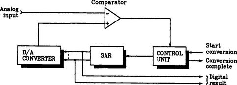
FIGURE 8.16 A functional block diagram of a successive-approximation analog-to-digital converter circuit.
The analog input signal provides one input to a voltage comparator. The second input comes from the output of a D/A converter. The input to the D/A converter is provided by an addressable latch called the successive approximation register (SAR). Each bit of this register can be selectively set or cleared by the control unit. The control unit can be an internal portion of an integrated circuit, or it may be a complete microprocessor system. In any case, the overall operation of the successive approximation converter is described.
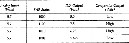
Let us suppose that the analog input voltage is 5.7 volts. Let us further suppose that the SAR and D/A converters are 4-bit devices that provide 0.625 volts per step at the output of the D/A converter. Finally, let us assume that the SAR is initially set to 1000, thus producing a 5-volt output for the D/A converter.
Under these conditions, the output of the comparator will be low, since the analog input (inverting input) is higher than the D/A output voltage (noninverting input). The control unit interprets this to mean that the SAR value is too low, and it then leaves the MSB (b3) alone and also sets the next bit (b2). The SAR now holds the binary value of 1100, which converts to 7.5 volts at the output of the D/A converter. Since this exceeds the value of analog input voltage, the comparator output will go high. The control unit interprets this to mean that the SAR value is too high.
The control unit then resets bit b2 (since that is what caused the excessive value) and sets the next most significant bit (b1). The SAR value of 1010 is now applied to the D/A converter to produce a comparator input of 6.25 volts. This is still higher than the analog input voltage, so the comparator output remains high. The control unit again interprets this to mean that the SAR value is too large.
The control unit then resets bit b1 and sets the next lower bit (b0), thus yielding an SAR value of 1001. This converts to 5.625 volts at the output of the comparator. Since this is still lower than the analog input, b0 will remain set. The conversion complete signal is now generated, indicating a completed conversion. The result (1001) is available in the SAR.
In general, the control unit starts by setting the most significant bit and monitoring the output of the comparator. This bit will then be left set or will be reset as a function of the state of the comparator. In either case, the same process is applied to the next lower bit and so forth until the least significant bit is left either set or reset. With each progressive step, the approximation gets closer. Regardless of the magnitude of the analog input voltage (within the limits of the converter), it will always take as many clock periods to convert the voltage as there are bits in the converted number. In this example, the successively better approximations were as listed in Table 8.4.
There is a striking similarity between the logic used during the successive approximation process and the logic applied during a split-half troubleshooting exercise. In both cases, each successive step reduces the number of options by one-half.
There are many integrated forms of A/D converters that utilize the successive approximation technique. One such device is the ADC-910, which is a 10-bit converter manufactured by Analog Devices, Inc. It provides a 10-bit result in 6 microseconds and is compatible with microprocessors. It should also be pointed out that all functions represented in Figure 8.16, except for the comparator and D/A converter, can be implemented with software internal to a microprocessor. However, the speed is generally much slower than a dedicated converter.
REVIEW QUESTIONS
1. A certain A/D converter has a 12-bit resolution specification for the analog input range of 0 to 10 volts. What is the smallest voltage change that can be represented in the output?
2. If the binary output of an A/D converter does not numerically increase with every increase in input voltage, we say the converter is ____.
3. The total time required for an A/D converter to obtain a valid digital output for a given analog input is called ____.
4. Contrast and explain the terms acquisition time and aperture time with reference to sample-and-hold circuits.
5. Would a weighted D/A converter be the best choice for a 64-bit converter circuit? Explain your answer.
6. What type of A/D conversion circuit provides the fastest conversion times? What are its disadvantages?
7. If a certain successive approximation A/D converter requires 10 microseconds to resolve a 0-volt to 2-volt step change on the input, how long will it take to resolve a 0-volt to 5-volt step change?
8. Repeat question 7 for a tracking A/D converter.
9. The use of a sample-and-hold circuit greatly reduces the highest usable frequency for an A/D converter. (True or False)
10. Discuss the relationship between droop rate in a sample-and-hold circuit and the necessary conversion time of a subsequent A/D converter circuit.