Amplifiers
2.1 AMPLIFIER FUNDAMENTALS
This chapter focuses on the analysis and design of several basic amplifier circuits. Not only is the amplifier circuit a fundamental building block in linear circuits, but the analytical techniques introduced in this chapter will greatly enhance your ability to analyze the circuits presented in subsequent chapters. Regardless of the specific circuit application (e.g., summing circuit, active filter, voltage regulator, and so forth), the op amp itself is simply an amplifier. Therefore, a thorough understanding of op amp behavior in circuits designed specifically as amplifiers will provide us analytical insight that is applicable to nearly all op amp circuits.
An amplifier generally accepts a small signal at its input and produces a larger, amplified version of the signal at its output. The gain (A) or amplification is expressed mathematically as
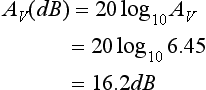
We may speak of voltage gain, current gain, or power gain. In each of these cases the above equation is valid. If, for example, a particular voltage amplifier produced a 5-volt RMS output when provided with a 2-volt RMS input, we would compute the voltage gain as
There are no units for gain; it is simply a ratio of two numbers. It is also convenient to express a gain ratio in its equivalent decibel (dB) form. The conversion equations are listed below:
The voltage gain of 2.5 on the amplifier discussed in the prior example could be expressed in decibels by applying Equation (2.2):
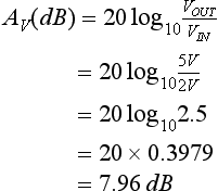
Thus, we see that an amplifier with a voltage gain of 2.5 also has a voltage gain of 7.96 dB. It should be noted that, technically, the equations cited previously for calculating voltage and current gains in their decibel form require that the input and output impedances be equal. In practice, this is rarely the case. Despite this known error, it is common in the industry to calculate and express the gains as described.
You should also be reminded that fractional gains (i.e., losses) are expressed as negative decibel values.
2.1.2 Frequency Response
The frequency response of an amplifier describes how its amplification varies with changes in frequency. We often communicate the frequency response of an amplifier in graphical form. Figure 2.1 shows a typical frequency response curve.
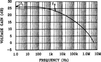
FIGURE 2.1 The bandwidth of an amplifier is the range of frequencies between the upper (fU) and lower (fL) cutoff frequencies.
The vertical axis indicates the amplifier’s voltage gain expressed in decibels. The horizontal axis shows the input frequency range.
The frequency response curve shown in Figure 2.1 indicates that the amplifier provides greater gain for low frequencies. Once the input frequency exceeds a certain value, the amplification begins to reduce significantly. Frequencies that are amplified to within 3 dB of the maximum output voltage level are considered as having passed the amplifier. Any frequency whose output voltage is lower than the maximum output voltage by more than 3 dB is considered to have been rejected by the amplifier. The frequency that separates the passband frequencies from the stopband frequencies is called the cutoff frequency. And since -3 dB corresponds to a power ratio of 0.5, the cutoff frequency is also called the half-power point on the frequency response curve.
The bandwidth of an amplifier is measured between the two half-power points. If the frequency response of an amplifier extends to include 0 (i.e., DC), then the bandwidth of the amplifier is the same as the upper cutoff frequency. This is the case for the amplifier represented in Figure 2.1. Here the lower frequency range extends all the way to 0, but in many circuits there will be a lower cutoff frequency that is greater than DC. The bandwidth is expressed as
where fU and fL are the upper and lower cutoff frequencies, respectively.
2.1.3 Feedback
So far in our discussions of op amps, we have considered only the behavior of the op amp itself with no external components. The op amp has been examined only in its open-loop configuration. In most practical applications, a portion of the amplifier’s output is returned through external components to the input of the amplifier. The return signal, called feedback, is then mixed with the incoming signal to determine the effective signal applied to the input of the op amp.
The amplitude, frequency, and phase characteristics of the feedback signal can dramatically alter the behavior of the overall circuit. If the feedback signal has a phase relationship that is additive when mixed with the incoming signal, we refer to the return signal as positive feedback. On the other hand, if the feedback signal is out of phase (optimally 180 degrees) with the input signal, then the effective input signal is reduced and we label it negative feedback. Both forms of feedback are useful in certain op amp applications, but for the remainder of this chapter we will limit our attention to negative feedback.
The external components that provide the feedback path may be frequency selective. That is, if some frequencies pass through the feedback circuit with less attenuation than other frequencies, then we have frequency-selective feedback. This is a very useful form of feedback, but for the remainder of this chapter we will limit our discussion to nonselective feedback methods.
2.2 INVERTING AMPLIFIER
The first circuit we will examine in detail is the inverting amplifier, one of the most common op amp applications. Figure 2.2 shows the schematic diagram of the basic inverting amplifier.

2.2.1 Operation
Under normal operation, an amplified but inverted (i.e., 180° phase shifted) version of the input signal (vI) appears at the output (vO). If the input signal is too large or the amplifier’s gain is too high, then the output signal will be clipped at the positive and negative saturation levels (±VSAT).
Now let us understand how the negative feedback returned through RF affects the amplifier operation. To begin our discussion, let us momentarily freeze the input signal as it passes through 0 volts. At this instant, the op amp has no input voltage (i.e., vD = 0 volts). It is this differential input voltage that is amplified by the gain of the op amp to become the output voltage. In this case, the output voltage will be 0.
Now suppose the output voltage tried to drift in a positive direction. Can you see that this positive change would be felt through RF and would cause the inverting pin (−) of the op amp to become slightly positive? Since essentially no current flows in or out of the op amp input, there is no significant voltage drop across RB. Therefore the (+) input of the op amp is at ground potential. This causes vD to be greater than 0 with the (−) terminal being the most positive. When vD is amplified by the op amp it appears in the output as a negative voltage (inverting amplifier action). This forces the output, which had initially tried to drift in a positive direction, to return to its 0 state. A similar, but opposite, action would occur if the output tried to drift in the negative direction. Thus, as long as the input is held at 0 volts, the output is forced to stay at 0 volts.
Now suppose we allow the input signal to rise to a +2 volt instantaneous level and freeze it for purposes of the following discussion. With +2 volts applied to RI and 0 at the output of the op amp, the voltage divider made up of RF and RI will have two volts across it. Since the (−) terminal of the op amp does not draw any significant current, the voltage divider is essentially unloaded. We can see, even without calculating values, that the (−) input will now be positive. Its value will be somewhat less than 2 volts because of the voltage divider action, but it will definitely be positive. The op amp will now amplify this voltage (vD) to produce a negative-going output. As the output starts increasing in the negative direction, the voltage divider now has a positive voltage (+2 volts) on one end and a negative voltage (increasing output) on the other end. Therefore the (−) input may still be positive, but it will be decreasing as the output gets more negative. If the output goes sufficiently negative, then the (−) pin (vD) will become negative. If, however, this pin ever becomes negative then the voltage would be amplified and appear at the output as a positive going signal. So, you see, for a given instantaneous voltage at the input, the output will quickly ramp up or down until the output voltage is large enough to cause vD to return to its near-0 state. All of this action happens nearly instantaneously so that the output appears to be immediately affected by changes at the input.
We can also see from Figure 2.2 that changes in the output voltage receive greater attenuation than equivalent changes in the input. This is because the output is fed back through a 10-kilohm resistor, but the input is applied to the 1.0-kilohm end of the voltage divider. Thus, if the input makes a 1-volt change, the output will have to make a bigger change in order to compensate and force vD back to its near-0 value. How much the output must change for a given input change is strictly determined by the ratio of the voltage divider resistors. Therefore, since the ratio of output change to input change is actually the gain of the amplifier, we can say that the gain of the circuit is determined by the ratio of RF to RI.
Recall that the internal gain (open-loop gain) of the op amp is not a constant. It varies with different devices (even with the same part number), it is affected by temperature, and it is different for different input frequencies. Now that we have added feedback to our op amp, the overall circuit gain is determined by external components (RF and RI). These can be quite stable and relatively unaffected by temperature, frequency, and so on.
If the input signal is too large or the ratio of RF to RI is too great, then the output voltage will not be able to go high enough (positive or negative) to compensate for the input voltage. When this occurs, we say the amplifier has reached saturation, and the output is clipped or limited at the ±VSAT levels. Under these conditions the output is unable to rise enough to force vD back to its near-0 level. From this you can safely conclude the following important rules regarding negative feedback amplifiers:
1. If the output is below +VSAT and above −VSAT, then vD will be very near 0 volts.
2. If vD is anything other than near 0 volts, then the amplifier will be at one of the two saturation voltages (±VSAT).
When the feedback and input resistor combination in Figure 2.2 are viewed as an unloaded voltage divider, it is easy to determine current flow. Since we know that no significant current is allowed to enter or leave the (−) pin of the op amp, we can conclude that any current flowing through RI must also pass through RF. The polarity of the input and output voltages will determine the direction of this current, but it is important to realize that the value of current through RI is the same as the current through RF.
Since very little current flows in or out of the input terminals of the op amp, we saw that there was essentially no voltage drop across RB which caused the (+) input terminal to remain at ground potential. Since vD is always near 0 as long as the amplifier remains unsaturated, this means that the (−) input terminal must also remain very near to ground potential. This is an important concept. Although the (−) input is not actually grounded, it remains very near ground potential. We commonly refer to this point in the circuit as virtual ground.
RB is included to compensate for errors caused by the fact that some bias current does flow in or out of the op amp terminals. Even though this bias current is small, it can cause a slight voltage drop across RF and RI. This voltage drop is then amplified and appears at the output of the op amp as an error voltage. By including RB in series with the (+) terminal and making its value equal to the parallel combination of RF and RI, we can generate a voltage that is roughly equal, but the opposite polarity from that caused by the drop across RF and RI. The error is generally reduced substantially but will be reduced to 0 only if the bias currents in the two input terminals happen to be equal. We will discuss this in greater detail in Chapter 10.
2.2.2 Numerical Analysis
Let us now learn to analyze the performance of the inverting amplifier circuit. We will calculate all of the following:
4. Slew-rate limiting frequency
5. Maximum output voltage swing
6. Maximum input voltage swing
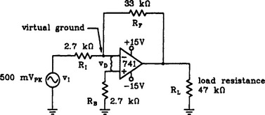
For purposes of our first numerical analysis exercise, let us evaluate the performance of the circuit in Figure 2.3.
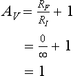
Voltage Gain.
You will recall that the voltage gain for this circuit is determined by the ratio of RF to RI or simply
The minus sign is used to remind us of the phase inversion since this is an inverting amplifier. Do not interpret the minus as a loss or a reduction in signal strength. For the circuit in Figure 2.3 the voltage gain will be
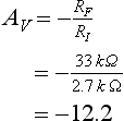
We can express this as a decibel gain by applying Equation (2.2):
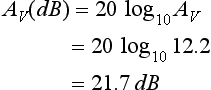
In this conversion, we must be particularly careful not to include the minus sign as part of the voltage gain. First, we will be unable to compute the logarithm. Second, if we tried to put the minus sign in after the calculation the resulting negative decibel answer would be misinterpreted as a loss.
It is important to note that the voltage gain computed in this section is the ideal closed-loop voltage gain of the circuit. The actual circuit gain will roll off as the input frequency is increased. This effect is discussed below as part of the discussion on bandwidth.
Input Impedance.
The input impedance of the amplifier shown in Figure 2.3 is that resistance (or impedance) as seen by the source (vI). You will recall that the voltage between the (+) and (−) terminals of the op amp (vD) will always be about 0 unless the amplifier is saturated. Since the (+) terminal is connected to ground (via RB) in the inverting amplifier circuit, it is reasonable to assume that the (−) pin will always be near ground potential even though it is not and cannot be connected directly to ground. But, since the (−) input is essentially at ground potential we call this point in the circuit a virtual ground.
Considering that the (−) pin is a virtual ground, it becomes apparent that the input impedance seen by the source is simply RI. That is, as far as current demand is concerned, resistor RI is effectively connected across the signal source. The equation for input impedance then is given by Equation (2.7).
For the case of the inverting amplifier shown in Figure 2.3, the input impedance is computed as follows:
In general, as long as the (−) pin remains at a virtual ground potential, the input impedance will be equal to the impedance between this pin and the source. If the impedance is more complex (e.g., resistor capacitor combination), then you must use complex numbers to represent the impedance. The basic method, however, remains the same.
Input Current Requirement.
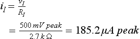
Ohm’s Law can be used to calculate the amount of current that must be supplied by the source. Recall that essentially no current flows into or out of the (−) terminal of the op amp. Therefore the only current supplied by the source is that drawn by RI. Since RI is effectively in parallel with the source due to the effect of the virtual ground, the input current can be computed as follows:
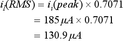
Since this is a sinusoidal waveform, we could easily convert this to an RMS value if desired as shown:
In our present case, the RMS value is found as follows:
As long as the input source can supply at least this much current without reducing its output, the op amp circuit will not load the source.
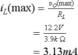
Maximum Output Voltage Swing.
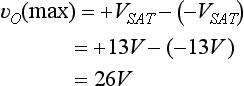
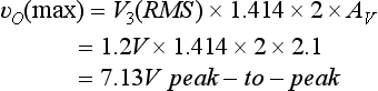
The output voltage of an op amp is limited by the positive and negative saturation voltages. These can both be approximated as 2 volts less than the DC supply voltage. Since the DC supply in Figure 2.3 is ±15 volts, the saturation voltages will be +13 volts and -13 volts for the positive and negative limits, respectively. Thus, the maximum output voltage swing is computed as follows:
For the circuit in Figure 2.3, the maximum output voltage swing is found as shown:

Since both DC supplies are equal, the output can swing equally above and below 0. This is the normal condition.
If you desire to be more accurate in the estimation of output saturation voltage, you may refer to the manufacture’s data sheet in Appendix 1. The manufacturer lists minimum and typical output voltage swings for different values of load resistance.
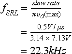
Slew-Rate Limiting Frequency.
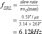
It should also be noted that the above maximum output is only obtainable for frequencies below the point where slew rate limiting occurs. This frequency can be estimated with the following equation:
In the case of the circuit being considered, the highest frequency that can produce a full output swing without distortion caused by slew rate limiting is computed as
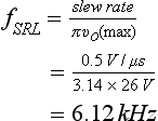
If we attempt to amplify frequencies higher than 6.12 kilohertz (and full amplitude) with the circuit shown in Figure 2.3, then the output will be nonsinusoidal. Once the input frequency goes higher than a certain frequency (about 9 kilohertz in this case), then the output amplitude begins to drop in addition to the distorted shape.
Maximum Input Voltage Swing.
We have computed the voltage gain of the circuit, and we know the maximum output voltage swing. We, therefore, have enough information to compute the largest input signal that can be applied without driving the amplifier into saturation.
Calculations for the present case are shown below:
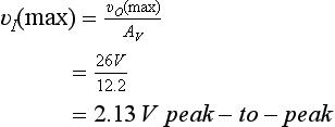
Since we are working with sinusoidal waveforms, we might choose to express this value as peak or RMS as shown below:
For our present circuit, we have

So, for the amplifier circuit presented in Figure 2.3, input signals as great as 756.5 millivolts RMS can be amplified without saturation clipping. If you attempt to amplify larger signals, then the peaks on the output waveform will be flattened at the output saturation voltage limits.
Output Impedance.
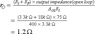
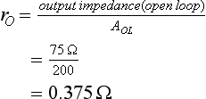
You will recall from Chapter 1 that the output impedance of an op amp is generally quite low. The data sheet in Appendix 1 lists 75 ohms as a typical output resistance for a 741 op amp. This value, however, is the open-loop output resistance. When negative feedback is added to the amplifier (as in Figure 2.3) the effective output impedance decreases sharply. The value of effective output impedance can be approximated as shown:
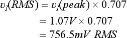
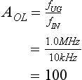
where AOL is the open loop gain of the op amp at the specified frequency. This can be read from the manufacturer’s graphical data (see Appendix 1) showing open-loop gain as a function of frequency. Alternatively, you may estimate it as
where fIN is the specific input frequency being considered.
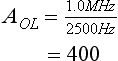
For the circuit in Figure 2.3, the closed-loop output impedance can be estimated at 1000 hertz as follows. First we compute the open-loop gain at 1000 hertz by applying Equation (2.16):
Next compute the effective output impedance with Equation (2.15):

This low value approaches our ideal value of 0 ohms. Now, as an illustration, recompute the value of output impedance at a higher frequency of 5 kilohertz.
First compute AOL with Equation (2.16).
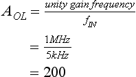
Next compute the effective output impedance with Equation (2.15).
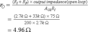
This value is significantly higher than our first estimate and clearly shows the increase in output resistance as the input frequency is increased.
How does a particular value of output impedance affect the performance of the amplifier circuit? To understand the effects, we can examine the equivalent circuit shown in Figure 2.4. Here we see a voltage source labeled vO driving a series circuit.
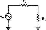
FIGURE 2.4 The equivalent output circuit of an op amp can be used to judge the effects of output impedance (rO).
The vO source is that voltage that would be present at the output of the op amp if the output impedance were truly 0 ohms. You can see that this ideal voltage (vO) is divided between the output impedance (rO), which is internal to the op amp, and RL, which is the op amp load. The voltage reaching the load can be computed with the voltage divider equation.
Let us compute the actual load voltage in Figure 2.3 at a frequency of 5 kilohertz. First we compute the ideal output voltage Equation (2.1):

We have found the value of rO at 5 kilohertz to be 4.96 ohms. Using the method shown in Figure 2.4, we can now determine the actual load voltage with Equation (2.17).
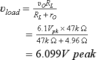
At a frequency of 5 kilohertz when the output resistance has increased to nearly 5 ohms, the effect of nonideal output resistance is minimal. Problems could be anticipated when the output resistance exceeds 1 percent of the value of load resistance.
Although the preceding calculation illustrates the effects of output resistance, it is valid only if we are below the frequency that causes slew rate limiting (fSRL). If fSRL is exceeded, we can expect the actual output to be much lower than the value computed with Equation (2.17), and the output will be nonsinusoidal in shape. Additionally, this method is inappropriate if the output drive capability of the op amp is exceeded.
Output Current Capability.
The output of the op amp in Figure 2.3 must supply two currents: the current through the feedback resistor (iF) and the current to the load resistor (iL). It is the sum of these currents that flows into or out of the output of the op amp.
The output of many (but not all) op amps is short circuit protected. That is, the output may be shorted directly to ground or to either DC supply voltage without damaging the op amp. For a protected op amp (such as the 741), the output current capability is not determined by the maximum allowable current before damage, but rather depends on the amount of reduced output voltage the application can tolerate.
With no output current being supplied to the load, the output voltage stays at the expected vO level, and the total output current is equal to iF. As the load current is increased (load resistance decreased), the actual output voltage begins to drop as shown in the previous section. Finally, if the load resistance is reduced all the way to 0 ohms, the output current will be limited to a safe value. This value can be found in the data sheet (Appendix 1), and is 20 milliamps for the 741 device.
As the load resistance varies from infinity (open) to zero (short), the output current from the op amp varies from iF to 20 milliamps. The limiting factor is the amount of reduction that can be tolerated on the output voltage.
The amount of current (iF) flowing through the feedback resistor is easily computed with Ohm’s Law as
On an unprotected op amp, the value of load current plus the value of feedback current must be kept below the stated output current rating. If this value is not supplied in the data sheet, then it can be estimated by using the maximum power dissipation data; recall that power = voltage × current.
Minimum Value of Load Resistance.
The minimum value of load resistance is determined by the maximum value of output current (determined in the previous section). The actual computation is essentially Ohm’s Law:
where iL is the maximum allowable output current of the op amp minus the current (if) flowing through the feedback circuit, and vL is the minimum acceptable output voltage.
Note that in many, if not most, applications, the value of output current needed for the load is substantially below the limiting value, so no significant loading occurs.
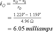
Let us assume that the application shown in Figure 2.3 requires us to have at least 1.19 volts across the load when 100 millivolts is applied to the input terminal. Let us further assume that the frequency of interest is 5 kilohertz. From previous calculations we know that the voltage gain (AV) is 12.2 (ignoring the effects of bandwidth described in the next section) and that the output resistance at 5 kilohertz is 4.96 ohms.
Figure 2.5 shows the equivalent circuit at this point. The value of iO can be computed with Ohm’s Law.

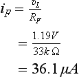
The value of iF can also be computed using Ohm’s Law, Equation (2.18).
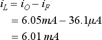
Kirchhoff’s Current Law can now be used to determine the value of load current (iL).
Calculations for the present example are shown below:
Using Ohm’s Law, Equation (2.19), we can now compute the value of RL.
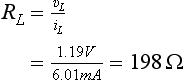
With this small value of load resistance, we would not be able to provide full-range voltage swings on the output because of excessive loading.
In the foregoing calculations (as with most calculations presented in this book), it is not important to remember all of the equations. Rather, strive to understand the concept and realize that most of what we are discussing is centered on basic electronics principles that you learned when you studied introductory AC and DC circuits.
Bandwidth.
Although the bandwidth of an ideal op amp is considered to be infinite, the bandwidth of real op amps and the associate amplifier circuit are definitely restricted. In the case of the circuit shown in Figure 2.3, the lower cutoff frequency is essentially 0. That is, since the op amp responds all the way down to DC, and since there are no reactive components to reject the lower frequencies, the amplifier circuit will operate with frequencies as low as DC.
The upper cutoff frequency is quite a different story. Figure 2.6 shows the open-loop frequency response (upper curve) for a 741 op amp. This is the same curve presented in the manufacturer’s data sheet as open-loop voltage gain as a function of frequency. Also drawn on the graph in Figure 2.6 is a line showing a voltage gain of 12.2. This is the ideal closed-loop gain that we calculated for the circuit in Figure 2.3.
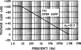
Notice that the difference between the open- and closed-loop gain curves is maximum at low frequencies. As the frequency increases, the difference between the two curves becomes less. Near the right side of the graph, the two curves actually intersect. What really happens to the overall circuit gain as the frequency increases?
The derivation of the formula for amplifier voltage gain (AV = −RF/RI) was based on the assumption that the op amp had an infinite (or at least a very high) voltage gain. This allowed us to make the assumption that the differential input voltage (vD) was 0. As you can see from the graph in Figure 2.6, our assumptions are reasonable for low frequencies. That is, the open-loop voltage gain is very high. But as the frequency increases and the open-loop gain rolls off, our assumptions begin to lose their validity. The most obvious proof of this exists beyond the point of intersection of the open- and closed-loop curves. In the region to the right of the intersection point, the open-loop gain is actually lower than our calculated closed-loop gain, thus making it impossible for our circuit to deliver the desired amplification.
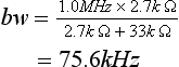
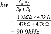
It is common to compute bandwidth in a circuit like that shown in Figure 2.3 by applying the following equation:
where fUG is the unity gain frequency of the op amp. Substituting values and computing gives us the following:
The actual frequency response for the circuit shown in Figure 2.3 is plotted in Figure 2.7. This represents the circuit’s real behavior. Two additional lines are superimposed on the plot for reference: the open-loop frequency response curve of the 741 op amp and the ideal gain curve of the circuit in Figure 2.3.
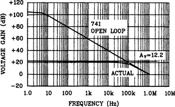
FIGURE 2.7 Actual frequency response of the circuit shown in Figure 2.3.
Power Supply Rejection Ratio.
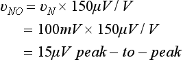
If the DC supply lines (V+ and V−) have noise, particularly high-frequency noise, these noise signals may affect the output signal. The degree to which the op amp is affected by the power supply noise is called the power supply rejection ratio (PSRR). The manufacturer’s data sheet normally expresses this parameter in microvolts per volt. To determine the magnitude of the noise signal on the output for a given amplitude of noise signal on the supply lines, we can use the following calculation:
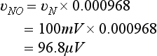
where vNO, vN, RF, RI, and PSRR are the values of the output noise signal, the noise signal on the DC supply lines, the feedback resistor, the input resistor, and the power supply rejection ratio, respectively. For example, refer to Figure 2.8.

FIGURE 2.8 An inverting amplifier circuit used to demonstrate the effects of the power supply rejection ratio.
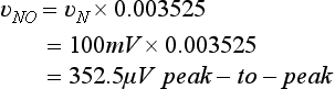
The manufacturer’s data sheet in Appendix 1 for a 741 op amp lists the power supply rejection ratio as ranging from 30 to 150 microvolts per volt. Thus, the worst-case effect on the output voltage for the circuit in Figure 2.8 is computed with Equation (2.23) as

In other words, the amplitude of the power line noise (vN) will be reduced by a factor of 0.003525. This means, for example, that if the DC supply lines have noise signals of 100 millivolts peak-to-peak, then we can anticipate a similar signal in the output with an amplitude of about
2.2.3 Practical Design Techniques
The following design procedures will enable you to design inverting op amp circuits for many applications. Although certain nonideal considerations are included in the design method, additional nonideal characteristics are described in Chapter 10.
To begin the design process, you must determine the following requirements based on the intended application:
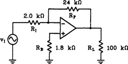
As an example of the design process, let us design an inverting amplifier with the following characteristics:
| 1. Voltage gain | 12 |
| 2. Maximum input current | 250 microamperes RMS |
| 3. Frequency range | 20 hertz to 2.5 kilohertz |
| 4. Load resistance | 100 kilohms |
| 5. Maximum input voltage | 500 millivolts RMS, 0-volt reference |
Determine an Initial Value for RI.
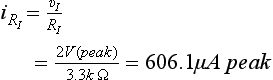
The minimum value for RI is determined by the maximum input voltage and the maximum input current and is computed with Ohm’s Law as follows:
In this case, the calculations are
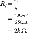
As a general rule, you should avoid designing amplifiers with input resistances of less than 1000 ohms unless you have a specific need for them. In our present case, the computed minimum (2.0 kilohms) is greater than 1000 ohms, so we will use the computed value. It should also be noted that the minimum input impedance is often determined by the needs of the application.
Determine the Value of RF.
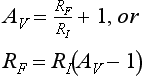
RF can be computed from the voltage gain equation, Equation (2.6):

Note that the inversion sign is omitted from the equation when computing a resistance value. For the present example, we compute RF as follows:
Determine the Required Unity Gain Frequency.
The minimum unity gain frequency for the op amp can be estimated by applying Equation (2.22). For the present case, we have

Since this is well below the 1.0-megahertz unity gain frequency of the 741, we should be able to use the 741 in this application (with regard to bandwidth).
Determine the Minimum Supply Voltages.
The minimum supply voltages are computed by simply ensuring that the maximum expected output voltage swing is no greater than the ±VSAT values. The maximum output swing can be found by using the basic equation, Equation (2.1), for voltage gain:
In our particular example, the maximum output voltage will be

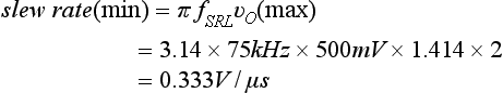
Notice the multiplying factor 1.414 to convert our input voltage (given in RMS) to a peak or worst-case value. The manufacturer’s data sheet in Appendix 1 indicates that the 741 op amp will produce at least a ±12-volt output swing with a ±15-volt supply voltage as long as the load resistor is at least 10 kilohms. Thus, we can infer that we have a worst-case internal voltage drop of 15 – 12, or 3 volts. This means that the minimum power supply voltage for our circuit must be higher than the maximum output voltage by the amount of the internal voltage drop (VINT). That is,
For our particular case, the minimum power supply voltages will be
Anything greater than ±11.48 volts for the DC supply will be adequate; therefore, let us choose the standard values of ±15 volts for our application.
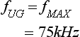
Determine the Required Slew Rate.
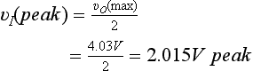
The required slew rate of the op amp is affected by the highest operating frequency and the maximum output voltage swing. In our present case, the highest input frequency has been specified as 2.5 kilohertz. The maximum peak-to-peak output voltage swing (vO(max)) was previously computed as 16.96 volts. The minimum required slew rate for the op amp is determined by rearranging Equation (2.11) to yield
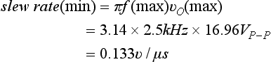
Since the slew rate of the 741 exceeds this minimum value, we can continue with our initial op amp selection. If the above calculation indicates a higher requirement than our preliminary op amp selection can deliver, then another op amp must be selected that has a higher slew rate.
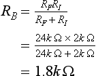
Calculate the Value of Compensation Resistor (RB).
The compensation resistor (RB) reduces the error in the output voltage caused by the voltage drops that result from the op amp’s input bias currents. To achieve maximum error reduction, we try to place equal resistances between both op amp input terminals and ground. If we were to apply Thevenin’s Theorem to the inverting input circuit, we would see that resistors RF and RI are effectively in parallel. This means that the optimum value for RB is simply the combined value of RF and RI in parallel.
For the present example, we compute RB as follows:
The final schematic is shown in Figure 2.9.
The actual behavior of the circuit is indicated in Figure 2.10 by an oscilloscope display. The measured performance is compared to the design goals in Table 2.1.
TABLE 2.1
| Parameter | Design Goal | Measured Value |
| Voltage gain | 12 | 11.7–12 |
| Frequency range | 20 Hz–2.5 kHz | <20 Hz to 2.5 kHz |

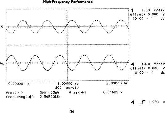
FIGURE 2.10 Oscilloscope displays showing the performance of the inverting amplifier shown in Figure 2.9. (Test equipment courtesy of Hewlett-Packard Company.)
2.3 NONINVERTING AMPLIFIER
Figure 2.11 shows the schematic diagram of a basic noninverting amplifier. As you might expect, the input signal is applied to the (+), or noninverting, input. Resistor RB is a compensation resistor similar to that described for the inverting amplifier. Because it has such a tiny current through it, we will ignore its effects for the immediate discussion.

Resistor RF and resistor RI form a voltage divider between the output terminal and ground. That portion of the output that appears across RI will provide the input to the (−) input terminal. The input signal (vI) supplies the voltage to the (+) input terminal. The difference between these two voltages (vD) is amplified by the open-loop gain of the op amp. Recall that as long as the output of the op amp is in the linear range (i.e., not saturated), the magnitude of vD will be very near 0 volts. Since the (+) input terminal is equal to vI, and since vD is approximately 0, we can conclude that the voltage on the (−) input terminal must also be nearly equal to vI. Recall that the source for the (−) input voltage is the output of the op amp. Now we see that the output will go as high as necessary in order to develop enough voltage drop across RI to equal vI.
Suppose, for example, that the input voltage (vI) made a sudden increase from 0 volts to some positive level. At this first instant, the (+) input of the op amp would be positive and the (−) input would still be at its previous 0-volt level. The voltage vD would now be amplified. Since the (+) input is more positive, the output rises as quickly as possible in the positive direction. As the output goes positive, a portion is fed back through the RF and RI voltage divider to the (−) input. Since the (−) input is becoming more positive, the value of vD is decreasing. That is, the two input terminal voltages are getting closer together. Finally, the output of the amplifier will stop going in the positive direction whenever the (−) input has come to within a few microvolts of the (+) input.
Now consider how high the output voltage had to go in order to bring the (−) input up to the same voltage as the (+) input. You can see that it is strictly the values of the voltage divider RF and RI that determine the amount of output voltage change required. Thus, for a given input voltage change, the output will make a corresponding change. The magnitude of the change is the gain of the amplifier and is largely determined by the ratio of RF to RI. This action is explained with mathematics in the following section.
Additionally note that as the input went positive, the output went positive. That is, the amplifier configuration is noninverting.
2.3.2 Numerical Analysis
Much of our analysis for the inverting amplifier is applicable to the noninverting amplifier circuit. We will determine a method to enable us to compute the following circuit characteristics:
For purposes of this discussion, let us analyze the noninverting amplifier circuit shown in Figure 2.12.
Voltage Gain.
We know by inspection of the circuit in Figure 2.12 that the voltage on the (+) input is approximately equal to vI. That is, there is no significant voltage drop across RB because the only current allowed to flow through RB is the op amp bias current (ideally 0). We also know from previous discussions that the voltage between the (+) and (−) input terminals (vD) is very near 0 volts. Thus, we may rightly conclude that the voltage on the (−) pin is approximately equal to the value of VI.
Ohm’s Law can be used to compute the current through RI as follows:
For the circuit in Figure 2.12, we have
Since negligible current flows into or out of the input of the op amp, we will assume that all of the current flowing through RI continues through RF, according to Kirchhoff’s Current Law. The voltage drop across RF can be computed by applying Ohm’s Law.

The output voltage can be determined through application of Kirchhoff’s Voltage Law. That is, we know the voltage on the (−) input is 2.0 volts peak. The output voltage will be greater than this by the amount of voltage drop across RF. It is computed as

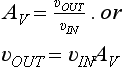
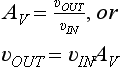
The voltage gain can be computed by the basic gain equation, Equation (2.1), as shown:

Recall from an earlier discussion that the voltage gain of the circuit is largely determined by the ratio of RF to RI. More specifically, the low-frequency or ideal voltage gain of the circuit can also be calculated with the following equation:
In our case, the calculations are

This latter method is the most common, but the former provides additional insight into circuit operation and the application of basic electronics principles.
The voltage can be expressed in decibels if desired, as we did with inverting amplifiers. In our present example, the equivalent voltage gain expressed in decibels is:
Note that the voltage gain computed in this section is the ideal closed-loop voltage gain of the circuit. The actual circuit gain will roll off as the input frequency is increased, just as it did with inverting amplifiers. This effect is discussed below as part of the discussion on bandwidth.
Input Impedance.
The input impedance of the noninverting amplifier circuit (refer to Figure 2.12) is essentially equal to the input impedance of the (+) input terminal of the op amp modified by the feedback effects. That is, the only current leaving the source must flow into or out of the op amp as bias current for the (+) input. The manufacturer’s data sheet for a 741 is shown in Appendix 1. It indicates that the input resistance is at least 0.3 megohms and is typically about 2.0 megohms. Recall that this is the effective resistance between the two op amp inputs. By considering the output impedance to be near 0, we can sketch the equivalent circuit shown in Figure 2.13(a).
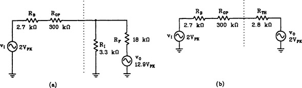
FIGURE 2.13 An equivalent circuit used to estimate the input impedance of the noninverting amplifier shown in Figure 2.12.
Let us make the following substitution for the value of vO:
This, of course, comes from Equation (2.1) and Equation (2.28). If we now apply Thevenin’s Theorem to the portion of the circuit to the right of the dotted line, we obtain the equivalent circuit shown in Figure 2.13(b). Notice that the resistance in our equivalent circuit has the same voltage (2 VPK) on both ends, which produces a net voltage of 0. If there is no voltage, there will be no current, so the effective input impedance is infinite. This represents the ideal condition.
In a real op amp circuit, the differential input voltage (vD) is greater than 0 and increases as the frequency increases. With reference to Figure 2.13(b), as the input frequency increases, the two voltage sources become more and more unequal. This causes a difference in potential across the resistance in the circuit, which in turn produces a current flow. The increasing current corresponds to a decreasing input impedance. Although the actual input impedance is quite high and can normally be assumed to be infinite, it can be approximated by the following equation:
where ROP is the value of input resistance provided by the manufacturer and AV is the open-loop voltage gain of the op amp. For the circuit shown in Figure 2.12, we can estimate input resistance at low frequencies as
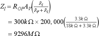
If we had used the more typical value of 2.0 megohms for the op amp resistance (ROP), we would have gotten a much higher value for input resistance. In either case, the actual effective input resistance is extremely high. This high input resistance is one of the primary advantages of the noninverting amplifier in many applications.
Input Current Requirement.
The input current can be estimated by applying Ohm’s Law to the input circuit as follows:

Even this is a worst-case value. If we had used the higher typical value for input resistance, we would have computed an even smaller value. For many, if not most, applications, this input current can be considered negligible. If it becomes necessary to consider this current, then additional considerations must be made because the exact value of input resistance varies considerably with temperature and frequency.
Maximum Output Voltage Swing.
As we found with the inverting amplifier, the output voltage of an op amp is limited by the ±VSAT levels. For most applications utilizing a bipolar op amp, the saturation voltages can be estimated at about 2 volts less than the DC supply voltage. In the case of Figure 2.12, we compute the maximum output swing, Equation (2.10), as

If a more accurate value is desired, the manufacturer’s data sheet can be used to find a more precise value for the worst-case saturation voltage.
Slew-Rate Limiting Frequency.
The highest frequency that can be amplified without distorting the waveform, because of the slew rate limitation of the op amp, is given by Equation 2.11.

If it is known for certain that the actual output swing will never be required to reach its limits, then the lower actual output swing can be used in place of vO(max) in the above calculation.
Maximum Input Voltage Swing.
The maximum input voltage swing is simply the highest input voltage that can be applied without driving the output past the saturation point. It is computed in the same manner as that for the inverting amplifier.

Since we are working with sinusoidal waveforms, we might choose to express this value as peak, as in Equation (2.13), or RMS, as in Equation (2.14), as shown:
If you attempt to amplify signals larger than 1.425 volts RMS, then the peaks on the output waveform will be flattened at the output saturation voltage limits.
Output Impedance.
You will recall from the analysis of the inverting amplifier that the effective output impedance decreases sharply from the open-loop value stated in the manufacturer’s data sheets. The value of effective output impedance can be approximated by applying Equation (2.15).
where AOL is the open-loop gain of the op amp at a particular frequency. For the circuit in Figure 2.12, the open-loop gain at 2500 hertz is computed with Equation (2.16) as
The output impedance at 2500 hertz can then be estimated as
In most cases, the output impedance is so low relative to the value of load resistance that the output voltage is essentially unaffected, but you can always be sure by performing the voltage divider calculation outlined in Section 2.2.2.
Output Current Capability.
If the output of the op amp is short-circuit protected (as in the 741), then the output current capability is limited by the maximum allowable drop in output voltage for the given application. This can be estimated with Ohm’s Law as discussed in the preceding section. Recall from our discussion of inverting amplifiers that the output must supply both load resistor current and the current through the feedback resistor. The feedback current is computed using Ohm’s Law. For this particular circuit, the calculations are

With no output current being supplied to the load, the output voltage stays at the expected vO level and the total output current is equal to iF. As the load current is increased (load resistance is decreased), the actual output voltage begins to drop because of the voltage divider action described in the previous section. Finally, if the load resistance is reduced all the way to 0 ohms, the output current will be limited to the short circuit value. This value can be found in the data sheet (Appendix 1) and is 20 milliamperes for the 741 device.
As the load resistance varies from infinity (open) to 0 (short), the output current from the op amp varies from iF to 20 milliamperes. The limiting factor is the amount of reduction that can be tolerated on the output voltage.
On an unprotected op amp, the value of load current plus the value of feedback current must be kept below the stated output current rating. If this value is not supplied in the data sheet, it can be estimated by using the maximum power dissipation data; recall that power = voltage × current.
Bandwidth.
The discussion of bandwidth presented for the inverting amplifier circuit is also applicable to the noninverting configuration. That is, as long as the circuit has no reactive components, the frequency response will extend all the way down to DC on the low-frequency end. We can estimate the high-frequency end of the frequency response by applying Equation (2.22):

Recall that the open-loop gain of the op amp falls off rapidly as the input frequency is increased above a few hertz. As the open-loop gain value approaches the computed closed-loop gain value, the actual circuit gain also begins to drop. Thus, we begin to experience increased errors in our gain calculations as the frequency is increased.
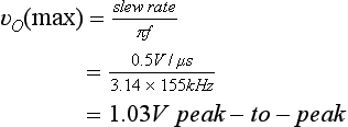
For these equations to be valid, it is important that the op amp output voltage swing be small enough to avoid the effects of slew rate limiting. The highest amplitude that can be amplified at a given frequency without the effects of slew rate limiting is given as
The slew rate is determined by the particular amplifier, f is the frequency of interest, and vO(max) is the highest peak-to-peak amplitude in the output before slew rate limiting begins to distort the signal. In the present case, if we try to operate at the upper cutoff frequency (155 kHz), we have to keep the output voltage below the value computed:
Power Supply Rejection Ratio.
The power supply rejection ratio provides us with an indication of the degree of immunity the circuit has to noise voltages on the DC power lines. The change in output voltage (vO) for a given change in DC power line noise voltage (vN) is computed with Equation (2.23):
where vO, vN, RF, RI, and PSRR are the values of the output noise signal, the noise signal on the DC supply lines, the feedback resistor, the input resistor, and the power supply rejection ratio (PSRR), respectively. The manufacturer’s data sheet in Appendix 1 lists the PSRR as ranging from 30 to 150 microvolts per volt. The worst-case effect on the output voltage for the circuit in Figure 2.12 is then
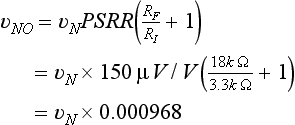
In other words, the amplitude of the power line noise (vN) will be reduced by a factor of 0.000968. This means, for example, that if the DC supply lines had noise signals of 100 millivolts peak-to-peak, we could anticipate a similar signal in the output with an amplitude of about
2.3.3 Practical Design Techniques
The following design procedures will enable you to design noninverting op amp circuits for many applications. Although certain nonideal considerations are included in the design method, additional nonideal characteristics are described in Chapter 10.
To begin the design process, you must determine the following requirements based on the intended application:
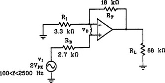
As an example of the design procedure, let us design a noninverting amplifier with the following characteristics:
| 1. Voltage gain | 8 |
| 2. Frequency range | DC to 5 kilohertz |
| 3. Load resistance | 27 kilohms |
| 4. Maximum input voltage | 800 millivolts RMS |
Determine an Initial Value for RI.
There are endless combinations of RF and RI that will produce the desired circuit voltage gain. The smaller the values of RF and RI, the higher the value of feedback current. The feedback current subtracts from the maximum available output current. Thus, we want to avoid extremely small values.
The larger we make RF and RI, the more the circuit operation is affected by certain nonideal characteristics. In general, neither resistor should be less than 1.0 kilohms nor more than 680 kilohms unless there is a compelling reason for them to be so. With this rule of thumb in mind, we select RI as 4.7 kilohms.
Determine the Value of RF.
RF can be computed from the voltage gain equation, Equation (2.28):
For the present design example, we compute RF as follows:
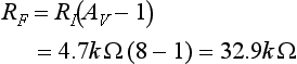
We select the nearest standard value of 33 kilohms to use as RF.
Determine the Required Unity Gain Frequency.
You will recall from our discussions on bandwidth that the error between the calculated or ideal gain and the actual gain increases as frequency increases. We can, however, estimate the required unity gain frequency by applying Equation (2.22).

Thus, we must select an op amp that has minimum unity gain frequency of at least 40.1 kilohertz. Since the 741 has a 1.0-megahertz unity gain frequency, it should be adequate for this application with respect to bandwidth.
Determine the Minimum Supply Voltages.
The minimum supply voltages are computed simply by ensuring that the maximum expected output voltage swing is no greater than the ±VSAT values. The maximum output swing can be found by using the basic equation for voltage gain, Equation (2.1).
In our particular example, the maximum output voltage will be
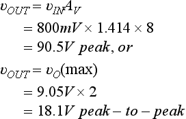
Notice the multiplying factor 1.414 to convert our input voltage (given in RMS) to a peak or worst-case value. The manufacturer’s data sheet in Appendix 1 indicates that the 741 op amp will produce at least a ±12-volt output swing with a ±15-volt supply voltage and a load resistance of at least 10 kilohms. Thus, we can infer that we have a worst-case internal voltage drop of 15 – 12, or 3 volts. The minimum power supply voltage can be determined with Equation (2.25):

Anything greater than ±12.05 volts for the DC supply will be adequate, so we choose the standard values of ±15 volts for our application. Realize that this is a worst-case calculation; a more typical internal drop would be 2 volts rather than 3 volts.
Determine the Required Slew Rate.
The minimum slew rate for the op amp is computed by transposing Equation (2.11).
Since the slew rate of the 741 exceeds this minimum value, we can continue with our initial op amp selection. If the above calculation indicates a higher requirement than our preliminary op amp selection can deliver, then another op amp must be selected that has a higher slew rate.
Calculate the Value of Compensation Resistor (RB).
The compensation resistor (RB) reduces the error in the output voltage caused by the voltage drops that result from the op amp’s input bias currents. As with the inverting configuration, we achieve maximum error reduction by inserting equal resistances between both op amp input terminals and ground. The resistance between the inverting input to ground is essentially equal to the parallel combination of RI and RF. This is easier to appreciate if you remember that the output impedance of an op amp is very low. For purposes of this analysis, assume that the output impedance is actually 0 ohms. In this condition, one end of both RI and RF connect to ground and the other ends connect to the inverting input terminal. Thus, they are effectively in parallel. The value of RB is calculated as in Equation (2.26):
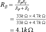
We will choose a standard value of 4.3 kilohms. The final schematic is shown in Figure 2.14.

The actual performance of the circuit is indicated by the oscilloscope plots in Figure 2.15. Additionally, Table 2.2 contrasts the measured performance with the original design goals.
TABLE 2.2
| Parameter | Design Goal | Measured Values |
| Voltage gain | 8 | 7.9–8.01 |
| Frequency range | DC–5 kHz | DC–>5 kHz |
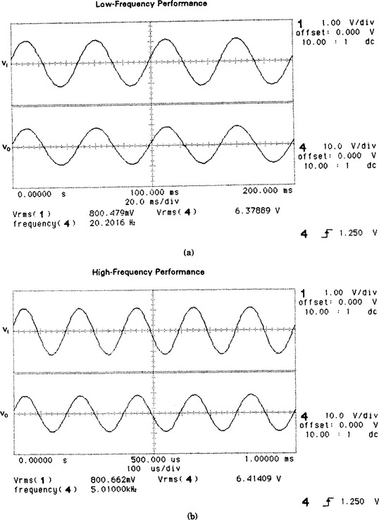
FIGURE 2.15 Oscilloscope displays showing the actual performance of the noninverting amplifier shown in Figure 2.14. (Test equipment courtesy of Hewlett-Packard Company.)
A slight phase shift can be seen between input and output waveforms in Figure 2.15. The effect is more pronounced as the input frequency is increased. For many applications, input/output phase relations are not important; in other applications they are critical. Chapter 10 discusses this issue in more detail.
2.4 VOLTAGE FOLLOWER
A voltage follower circuit using an op amp is shown in Figure 2.16. This is a very simple, but very useful, op amp configuration.

If you compare the voltage follower circuit to the noninverting amplifier previously discussed, you will see that RI and RF in the noninverting circuit have become respectively, infinity and 0 to form the follower circuit. Since there is no significant impedance in the path of the (−) input terminal, there is no need for the compensating resistor in the (+) terminal.
The voltage on the (+) input is equal to VI because of the direct connection. Recall that vD is approximately 0 volts as long as the amplifier is not saturated. This means that the (−) input terminal will also be approximately equal to VI. And, since the (−) pin is connected directly to the output, the output must also be equal to vI. Because the output is essentially equal to the input at all times, the voltage gain is unity (i.e., 1). The circuit is called a voltage follower because the output appears to follow or track the input voltage.
So, what is the value of a circuit that gives us an output voltage that is equal to the input? Well, although the voltage gain is only 1, there are other very important reasons for using a voltage follower. One of the most important uses for the circuit is for impedance transformation. By inspection, you can see that the input impedance is very high, as the only current drawn from the source is the bias current for the (+) terminal. The output impedance, on the other hand, is quite low. As with the other configurations previously studied, the output impedance approaches an ideal value of 0, so the voltage follower circuit can interface a high impedance device or circuit to a lower impedance device or circuit. Although very little current is drawn from the source, a substantial current may be supplied to the load.
2.4.2 Numerical Analysis
The numerical analysis for the voltage follower is simpler than for previous circuits because of the lack of circuit complexity. Let us analyze the circuit shown in Figure 2.16 and determine the following values:
For purposes of the following analyses, let us assume that the op amp in Figure 2.16 is a 741.
Voltage Gain.
The ideal voltage gain of a voltage follower circuit is always unity, or 1. This can be further demonstrated by applying the voltage gain equation, Equation (2.28), presented for the noninverting amplifier circuit. Since RF is now 0 and RI is infinity, our calculations become
As with other amplifier configurations, the actual gain of the circuit falls off at high frequencies. This is further discussed, along with bandwidth, in a later section.
Input Impedance.
The input impedance of the voltage follower is ideally infinite because it is essentially the input resistance of the (+) input of the op amp modified by the effects of feedback. The value may be estimated by applying Equation (2.29) with the quantity RI/(RF + RI) considered to be unity. Thus, for low frequencies (i.e., near DC) the circuit in Figure 2.16 will have a minimum input impedance of

If we had used typical values for ROP, we would have gotten an even higher value for ZIN. In any case, the value is so high that we can consider it as infinite for most applications.
Input Current Requirement.
The input current for the circuit in Figure 2.16 is only the bias current for the (+) input terminal. This is ideally 0 and for most applications may be neglected. If more precision is desired, then the manufacturer’s data sheet in Appendix 1 can be referenced. The data sheet indicates that the input bias current will be no higher than 500 nanoamperes, with a more typical value listed as 80 nanoamperes. Even though this current is temperature dependent, the absolute values are so small that they may be neglected in many applications.
Maximum Output Voltage Swing.
The maximum output voltage swing for the follower circuit is determined in the same manner, Equation (2.10), as that used with preceding amplifiers. That is,
If a more accurate value is desired, the manufacturer’s data sheet can be used to find a more precise value for the worst-case saturation voltage.
Slew-Rate Limiting Frequency.
As with the amplifier configurations discussed previously, the highest frequency that can be amplified with a full output voltage swing and no slew-rate limited distortion is computed as in Equation (2.11):

If it is known for certain that the actual output swing will never be required to reach its limits, then the lower actual output swing can be used to compute the slew-rate limiting frequency.
Maximum Input Voltage Swing.
Since the amplifier has a voltage gain of 1, the maximum input voltage swing is equal to the maximum output voltage swing. Thus, in the case of Figure 2.16, we could have an input signal as large as ±13 volts without causing the amplifier to saturate. Again, if you plan to push the amplifier to its limits, you should refer to the manufacturer’s data sheet and select the worst-case output saturation voltage at the worst-case temperature. The computations, however, remain similar.
Output Impedance.
The output impedance of the voltage follower can be computed as follows:
where AOL is the open-loop gain of the op amp at the specified frequency. You can determine the value of AOL at the desired operating frequency as in Equation (2.16):
where fIN is the specific input frequency being considered.
For the circuit in Figure 2.16, the open-loop gain at 5 kilohertz, for example, is

The output impedance then becomes Equation (2.31).
As with most op amp circuits, the output impedance is so low relative to any practical load resistance that its effects may be ignored.
Output Current Capability.
The total current flowing in or out of the output terminal of the op amp in Figure 2.16 may be delivered directly to the load. That is, the feedback current is extremely small and can be disregarded in nearly all cases. As the load resistance varies from infinity (open) to 0 (short), the output current from the op amp varies from 0 to the short-circuit value of 20 milliamps (given in the data sheet). The limiting factor is the amount of reduction that can be tolerated on the output voltage swing.
On an unprotected op amp, the value of load current must be kept below the stated output current rating. If this value is not supplied in the data sheet, it can be estimated by using the maximum power dissipation data; recall that power = voltage × current.
Bandwidth.
The bandwidth (i.e., the upper cutoff frequency) of a voltage follower circuit may be estimated by the following equation:
For the circuit shown in Figure 2.16, we can compute the upper cutoff frequency and/or bandwidth as follows:
At lower frequencies, the voltage gain will be nearly equal to the calculated value of unity. As the frequency approaches the upper cutoff, the voltage gain begins to decrease. Once the input frequency exceeds 1.0 megahertz (for a 741), the overall circuit gain will decrease dramatically.
Power Supply Rejection Ratio.
The change in output voltage (vO) for a given change in DC power line noise voltage (vN) is computed for the voltage follower with the following equation:
where vO, vN, and PSRR are the values of the output noise signal, the noise signal on the DC supply lines, and the power supply rejection ratio, respectively. The manufacturer’s data sheet in Appendix 1 lists the power supply rejection ratio (PSRR) as ranging from 30 to 150 microvolts per volt. The worst-case effect on the output voltage for the circuit in Figure 2.16 is then

In other words, the amplitude of the power line noise (vN) will be reduced by a factor of 0.000150. This means, for example, that if the DC supply lines had noise signals of 100 millivolts peak-to-peak, we could anticipate a similar signal in the output with an amplitude of about
2.4.3 Practical Design Techniques
The design of a voltage follower circuit is fairly straightforward because of the lack of circuit complexity. Let us examine the design procedure by designing a voltage follower with the following characteristics:
| 1. Input voltage range | 100 to 500 millivolts RMS |
| 2. Frequency range | DC to 75 kilohertz |
| 3. Load resistance | 4.7 kilohms |
| 4. Input resistance | greater than 100 kilohms |
| 5. Source impedance | 1.8 kilohms |
Select the Op Amp.
First, we must select an op amp that can provide unity gain up to the maximum input frequency. That means we will need an op amp with a unity gain bandwidth of at least Equation (2.32):
Second, the slew rate of the op amp must be adequate to allow the required output voltage swing at the highest input frequency. The required slew rate is given by Equation (2.11):
Since both the unity gain frequency and the slew rate requirements are within the limits of the 741 (see Appendix 1), let us choose this device for our design.
Select the Power Supply Voltages.
Now we must select a power supply voltage that is high enough to prevent saturation on the highest input voltage. The worst-case internal voltage drop on the output for a 741 is listed as 5 volts in Appendix 1 for load resistances between 2 and 10 kilohms. A more typical value is 2 volts. The minimum required power supply voltage can be determined as in Equation (2.25):
We will choose a more standard value of ±15 volts for our power supply voltages. The complete schematic of our voltage follower circuit is shown in Figure 2.17.

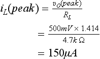
Now let us check to be sure the 741 can supply the required current to our load without causing an appreciable voltage loss in our output. When the output voltage reaches its maximum level, the load current can be computed with Ohm’s Law as
This should have negligible effect on the output voltage of the op amp because the 741 can supply significantly higher currents.
Figure 2.17 also illustrates the use of a compensating resistor RB. Recall from the previous amplifier designs that bias current in the op amp can cause output offsets because of the voltage drops across any resistances in line with the bias current. We minimize this offset by providing equal resistances in both (+) and (−) inputs. The resistance in the (+) input is simply the source resistance that was given as 1.8 kilohms. To minimize output errors, we insert an equal value RB in the feedback loop. Note that no significant signal current flows through RB. Therefore, the voltage gain is unaffected by the addition of RB, and it remains constant at unity.
The actual performance of our voltage follower circuit is shown in Figure 2.18 through the use of an oscilloscope plot. The measured performance is compared to the design goals in Table 2.3.
TABLE 2.3
| Parameter | Design Goal | Measured Values |
| Input resistance | >100 kΩ | >100 kΩ |
| Voltage gain | 1.0 | 0.97–0.99 |
| Frequency range | DC–75 kHz | DC–>75 kHz |

FIGURE 2.18 Oscilloscope displays showing the performance of the voltage follower circuit shown in Figure 2.17. (Test equipment courtesy of Hewlett-Packard Company.)
2.5 INVERTING SUMMING AMPLIFIER
Figure 2.19 shows the schematic diagram for an inverting summing amplifier. The summing amplifier has several inputs—the circuit in Figure 2.19 shows four with the possibility of others indicated. Although the input sources are shown as DC signals (i.e., batteries) the circuit works equally well for AC signals or even a combination of AC and DC signals.
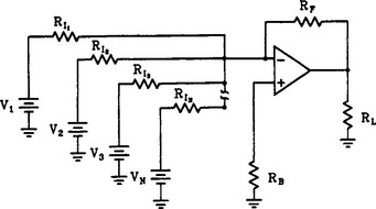
There are several ways to understand the operation of the inverting summing amplifier circuit. One simple method is an application of the Superposition Theorem. In this case, we consider the effects of each input signal one at a time with all other sources being set to 0. We know from our discussion of the basic inverting amplifier that the (−) input terminal is a virtual ground point. That is, unless the amplifier’s output is saturated, the voltage on the (−) input will be within a few microvolts of ground potential. Thus, when we replace all but one source with a short (i.e., set them to 0 volts), the associated input resistors essentially have a ground connection on both ends. In other words, one end of each resistor is connected to ground through the temporary short that we inserted across the battery as part of the application of the Superposition Theorem. The opposite end of each input resistor is connected to the (−) input, which we know is a virtual ground point. As all input resistors but one have ground potential on both sides, there will be no current flow through them and they can be totally disregarded for the remainder of our analysis.
By disregarding all input resistors and sources but one, we are left with a simple single-input inverting amplifier circuit. We already know how this circuit works, so we can now compute voltage gain, input current, output voltage, and so on, for this single input. We can then perform a similar analysis for each of the other inputs one at a time. The actual output voltage of the circuit is the combination or sum of the effects of the individual inputs.
One important point that should be recognized about the circuit shown in Figure 2.19 is that the gains for each input signal are independent. That is, the ratio of RF to RI1 will determine the voltage gain that signal V1 receives. V2, on the other hand, is amplified by a factor established by the ratio of RF and RI2. Thus, we can quickly conclude that the individual gains can be varied by changing the values of the input resistors, while the gains of all signals can be changed simultaneously by varying the value of RF. Consider, for example, that the circuit is being used as a microphone mixer. The signals from several microphones provide the inputs to the circuit. If the individual input resistors are variable, then they adjust the amplitude (i.e., volume) of one microphone relative to another. If the feedback resistor is also variable, it serves as a master volume control because it varies the amplification of all microphone signals but does not change the strength of one relative to another.
Resistor RB is a compensating resistor and ensures that both inputs of the op amp have similar resistances to ground. You will recall that this helps minimize problems caused by the op amp’s bias currents.
2.5.2 Numerical Analysis
We will now analyze the numerical performance of an inverting summing amplifier circuit. The circuit to be analyzed is shown in Figure 2.20. Compute the following characteristics of the circuit:

1. Voltage gain of each input signal
2. Input impedance of each input signal
3. Input current requirement for each input signal
4. Maximum output voltage swing (total)
Voltage Gain.
The voltage gain for each input signal in Figure 2.20 must be computed separately. Each gain, however, is computed in the same manner, Equation (2.6), as a simple inverting amplifier circuit. That is,
where the minus sign is used to remind us of the phase inversion given to each signal.
The individual voltage gains for the circuit in Figure 2.20 are computed:

Observe that each of these calculations is similar to our analysis on a single-input inverting amplifier and that the gains are independent of each other.
Input Impedance.
The input impedance seen by each input is equal to the value of the input resistor on that particular input. That is, since each input resistor connects to a virtual ground point, its respective source sees it as the total input impedance. No calculations are required to determine the input impedance; we simply inspect the input resistors’ individual values.
Input Current Requirement.
Each source must supply the current for its own input. The amount of current can be determined by Ohm’s Law and is simply the input voltage divided by the input resistance, Equation (2.8). For the circuit shown in Figure 2.20, we can compute the following values:

In the case of V1, a variable DC source, we computed the worst-case input current by using the maximum input voltage (3 volts). Similarly, for the alternating voltage sources v2 and v3, we used peak values of input voltage. In each of these cases, the source must be capable of supplying the required current.
Maximum Output Voltage Swing.
The output voltage of the summing amplifier is limited by the ±VSAT values. For the purposes of this analysis, we will estimate the values of ±VSAT to be 2 volts below the DC power supply values. The calculations, Equation (2.10), to determine the maximum output voltage swing are
As with previous circuits, we can utilize the data sheet supplied by the manufacturer if it becomes necessary to have a more accurate, or perhaps worst-case, value.
Maximum Input Voltage Swing.
The maximum input voltage swing of an amplifier is the voltage that causes the amplifier’s output to reach saturation. Input voltages that exceed this limit will produce distorted (i.e., clipped) output signals. In the case of the summing amplifier, the situation is more complex than with previous, single-input amplifiers. That is, the instantaneous level of output is determined by the instantaneous values of input voltage on all inputs. First we will consider each input separately to determine the maximum levels of an isolated input. The calculations, from Equation (2.1), are similar to those used with previous circuits.
where AV is the voltage gain received by a particular input. The individual calculations are
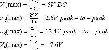
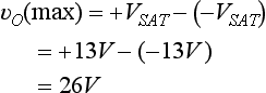
Note that the negative and positive saturation limits were used as the maximum output “swing” for V1 and V4, respectively, since these two inputs are DC and will only be limited by one saturation barrier.
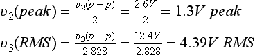
With reference to v2 and v3, we may want to express them in their peak and RMS forms to better compare them with the signals shown in Figure 2.20. These conversions are
Since the maximum limits on all inputs (both DC and AC) are greater than the values listed on the schematic, we will assume that no single input can cause the amplifier output to saturate. However, two or more input signals may combine at some instant to drive the output to its saturation limit. Let us determine if this situation can occur in the circuit shown in Figure 2.20. To perform this calculation, we want to determine the worst-case combination of input signals. First observe that V1 and V4 are of opposite polarity and thus tend to reduce each other’s effect in the output. A worst case would be when V1 is zero or when V1 is maximum (3 volts DC). Let us evaluate them with Equation (2.1) to determine the worst-case combination.
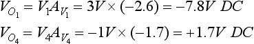
From these calculations we can see that if V1 were reduced to zero, V4 would produce +1.7 volts in the output. On the other hand, if V1 were set for maximum (3 volts DC), the net output voltage would be the difference between the V1-produced and V4-produced outputs. This worst-case output voltage is simply -7.8 + 1.7, or -6.1 volts.
Now we must consider the effects of the AC signals v2 and v3. The worst-case output condition will occur when these two inputs hit their peak values simultaneously and have the same polarity as V1. The output voltages produced individually by v2 and v3 are

The net effect of V1, v2, v3, and V4 can be found by adding the individual output values (Superposition Theorem).

Since this worst-case value is less than our maximum output voltage limit (±13 volts typically), we should not have a problem. In extreme cases, however, we may have a potential problem. Recall that the output limits of ±13 volts were obtained by using typical performance values for the 741. If worst-case values are used, we will find that the limits fall to ±10 volts under worst-case conditions. If this situation were to occur at the same time our inputs were all at their maximum values, we would drive the amplifier into saturation and produce a clipped output. If this is a serious concern for our particular application, we can reduce RF slightly to prevent the combined signals from driving the output to saturation.
Output Impedance.
The output impedance of the summing amplifier can be estimated as follows:
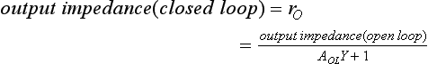
where AOL is the open-loop gain of the op amp at the specified frequency and Y is computed as follows:
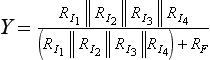
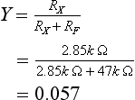
Now let us compute the output impedance for the circuit in Figure 2.20. First we compute the value of the parallel combination of input resistors (RX):

Then we use this value to compute the factor Y, Equation (2.35):
Next we determine the value of AOL at the frequency of interest, using Equation (2.16). We will use the worst-case value that occurs at the highest input frequency (10 kilohertz):
Finally we compute the estimated value of output resistance, from Equation (2.35):

Since this value was computed at the highest input frequency (worst case), and since it is very low compared to the value of the load resistor, its effects on output voltage can be safely ignored.
Output Current Capability.
The maximum value of load current occurs when the output reaches its highest instantaneous value. The maximum voltage was previously computed as 12.2 volts. The worst-case load current can be computed with Ohm’s Law:
The output of the op amp must also supply the feedback current. In most applications, this current can be ignored because it is generally much smaller than the load current. Our present circuit is no exception. That is, we can see by inspection that the feedback path has over 10 times as much resistance as the load.
The data sheet in Appendix 1 indicates that even under worst-case conditions, the output can maintain at least 10 volts across a 2000-ohm load. By Ohm’s Law, we can conclude that this corresponds to an output current of
Of course, the typical value of current is even higher. In any case, the current capability of the output clearly exceeds our requirements and therefore poses no problem. If our load resistor were smaller, we could anticipate a reduced output voltage.
Bandwidth.
For a meaningful discussion on bandwidth, we must consider the response of each input individually. When the responses are considered separately, we can estimate the bandwidth of any given input by applying the bandwidth equation, Equation (2.22), used in previous analyses:
We know from earlier calculations that the bandwidth will decrease as the closed-loop gain is increased. Let us calculate the bandwidth for the input in Figure 2.20 that has the highest gain. We have already determined the individual gains to be 2.6, 10, 2.1, and 1.7 for inputs V1 through V4. We will compute the bandwidth for the v2 input because its gain is the highest. Incidentally, there would be very little point in computing the bandwidth for inputs V1 and V4 because these have DC signals applied. The bandwidth for the v2 input is
A similar analysis could be made for input v3, which has a computed gain of 2.1 and a maximum input frequency of 10 kilohertz. For large amplitude output signals, the slew rate will tend to restrict the operation to even lower frequencies. This is discussed in the following section.
Slew-Rate Limiting Frequency.
As discussed for previous amplifier configurations, the slew rate also limits the highest operating frequency for larger output voltage excursions. The slew-rate limiting frequency is found as follows, Equation (2.11):
Thus, although the v2 input was shown to have a 90.9-kilohertz bandwidth as established by the unity gain frequency, the full-power upper limit is only 6.12 kilohertz. In the given application, however, the applied signal is only 5000 hertz, so this should not hamper the operation of the circuit with respect to the v2 input.
The v3 input, on the other hand, operates at 10 kilohertz. This means that we can never get the full 26-volt swing in the output as a result of v3 signals. The schematic indicates that the highest input voltage is 1.2 volts RMS. The gain for v3 was previously computed as 2.1. The largest normal output swing from v3 can be found by applying Equation (2.1):
The actual slew-rate limiting frequency for this input is then estimated with Equation (2.11) as
In the given circuit, the slew rate should not interfere with the expected operation.
2.5.3 Practical Design Techniques
To illustrate the design method for an inverting summing amplifier circuit, let us design a 3-input circuit with the following performance characteristics:
Input 1. 0 to 500 millivolts peak, at a frequency of 2.7 kilohertz. The source resistance is 1.0 kilohms, and the signal is to be amplified by a factor of −3.5.
Input 2. −2 to +2 volts DC. The source resistance is 0.75 ohms, and the voltage is to pass through the circuit without amplification (i.e., inversion only).
Input 3. 0 to 3 volts RMS, at a frequency of 500 hertz. The source resistance is 50 ohms, and the signal is to be amplified by a factor of −2.
Recall that the minus signs preceding the gain factors tell us that the signals are inverted in the process of being amplified. The negative gains do not imply voltage reduction.
The output of the amplifier must drive a load resistance that varies from 10 to 50 kilohms.
Determine the Worst-Case Input.
Our initial step is to determine which input to design first. If we choose the wrong one, we will end up recalculating some of our values. The proper input can be identified by choosing the one that has the highest product of source resistance multiplied by voltage gain (absolute value). These calculations are shown for comparison:
Since input 1 has the highest gain-source-resistance product, we will begin by selecting the input resistor for input 1.
Choose the Value for the First Input Resistor.
The source resistance and the input resistor are in series. Their sum in conjunction with RF will determine the voltage gain of that input. In theory, there is no requirement to have a physical resistor for RI—the source resistance alone can serve as the input resistor. In practice, however, the source resistance is usually only an estimate and rarely a constant; therefore, it is generally wise to include a separate resistor as RI and to make this resistor large enough to minimize the effects of changes in the source resistance. The application must dictate the degree of stability needed, but in general, if the input resistor is 10 times as large as the source resistance, then the effects of changes in the source resistance are reduced by about 90%. If greater protection is needed, increase RI accordingly.
For purposes of our sample design, let us choose RI1 to be 10 times the value of source resistance. The value of RI1 then is computed as

Calculate the Required Feedback Resistor (RF).
The feedback resistor is calculated by using a transposed version of the basic voltage gain equation, Equation (2.6), for an inverting amplifier.
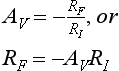
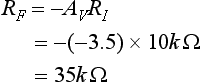
We choose the nearest standard (5% tolerance) value of 36 kilohms.
Compute the Remaining Input Resistors.
Values for each of the remaining input resistors can be calculated by using yet another transposed version of the basic voltage gain equation, Equation (2.6).

Using this equation, we can now compute values for RI2 and RI3 as follows:

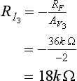
Compute the Value of RB.
To minimize the effects of op amp bias currents, we want to make the value of RB equal to the parallel combination of RF and all of the input/source resistors.
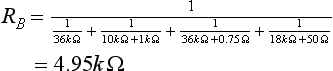
Determine the Required Power Supply Voltages.
The DC power supply voltages must be high enough to prevent saturation under the worst-case input conditions. Generally, the condition to be considered is when all inputs are at the maximum voltage at the same time. The worst-case output voltage, then, is computed by adding the output voltages caused by each of the individual inputs, as in Equation (2.1).
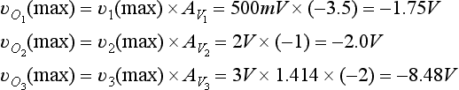
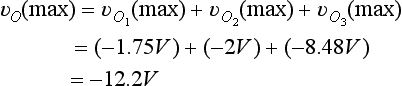
Unless the internal drop on the output of the selected op amp is unusually high, we should be able to use standard ±15-volt supplies. Suppose, for example, we decide to use a 741 op amp. The manufacturer’s data sheet in Appendix 1 indicates that the op amp can deliver at least ±12 volts to a load ≥10 kilohms when ±15-volt supplies are used. We will plan to use a 741 unless we encounter problems with bandwidth or slew rate (verified in subsequent sections).
Determine the Required Unity Gain Frequency.
The minimum unity gain frequency for each input is computed with Equation (2.22):

In all cases, the required minimum unity gain bandwidth is substantially below the 1.0-megahertz limit of a 741. Therefore, we will initially plan to use a 741 in our design. If the minimum bandwidth requirement were greater than 1.0 megahertz, we would have to select a different op amp.
Determine the Required Slew Rate.
The minimum acceptable slew rate for the op amp is given by the following equation, Equation (2.11):
Let us determine the minimum slew rate for each input:
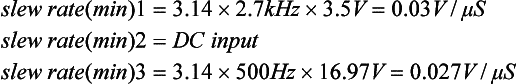
In all cases, the required slew rate is substantially below the 0.5-volts-per-microsecond rating of the 741. Therefore, we will select this device as our final choice.
The schematic of our design is shown in Figure 2.21. The actual performance of the circuit is evident from the oscilloscope displays in Figure 2.22. The measured performance is contrasted with the original design goals in Table 2.4.
TABLE 2.4
| Parameter | Design Goal | Measured Value |
| Voltage gain 1 | −3.5 | −3.27 |
| Voltage gain 2 | −1.0 | −1.0 |
| Voltage gain 3 | −2.0 | −1.99 |

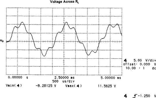
FIGURE 2.22 Oscilloscope display showing the actual performance of the inverting summing amplifier shown in Figure 2.21. (Test equipment courtesy of Hewlett-Packard Company.)
2.6 NONINVERTING SUMMING AMPLIFIER
Figure 2.23 shows a 3-input, noninverting summing amplifier circuit. Its operation is significantly more difficult to analyze than that of the inverting summing amplifier. In the present case, we will need to rely heavily on the use of Thevenin’s Theorem to analyze the operation of the circuit. First, though, let us examine the fundamental theory of operation.
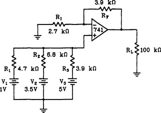
Although the network on the (+) input is somewhat difficult to analyze mathematically, we know intuitively that it must be equivalent to some value of voltage and some value of resistance. If we mentally replace the network on the (+) input with a simple voltage source and series resistance, we see that the circuit becomes a simple, familiar noninverting amplifier circuit. The gain of this equivalent circuit is determined by the ratio of RF to RI. So, with the single exception of the network on the (+) input, analysis of the circuit is quite straightforward.
2.6.2 Numerical Analysis
Now let us analyze the circuit shown in Figure 2.23 numerically. We will focus our efforts on the network associated with the (+) input terminal. If we can reduce this network to a simpler network consisting of a single voltage source and a single resistor, then we can analyze the rest of the circuit using the method presented for the simple noninverting amplifier.
To reduce the network on the (+) input, we apply Thevenin’s Theorem in two stages. First, simplify V1, V2, and the associated resistors. Figure 2.24(a) shows the circuit divided between V2 and V3. Application of Thevenin’s Theorem to the portion of the circuit on the left side of the break point gives us a Thevenin voltage (V′TH) of 2 volts and a Thevenin resistance (R′TH) of 2.78 kilohms. This equivalent circuit is shown in Figure 2.24(b) reconnected to the original V3/R3 circuit.

FIGURE 2.24 Thevenin’s Theorem is used to simplify the summing network for the noninverting summing amplifier.
If we apply Thevenin’s Theorem to the partially simplified circuit in Figure 2.24(b), we obtain the fully reduced equivalent circuit of Figure 2.24(c). Thus, the network of resistors and voltage sources on the (+) input of the summing amplifier originally shown in Figure 2.23 can be replaced by the Thevenin equivalent circuit shown in Figure 2.24(b). This substitution is shown in Figure 2.25.

FIGURE 2.25 The summing network shown in Figure 2.23 can be replaced by its Thevenin equivalent for analysis purposes.
We can now complete our analysis of the simplified circuit by applying techniques presented for the basic noninverting amplifier.
Voltage Gain.
The voltage gain of the circuit in Figure 2.25 can be computed with the noninverting amplifier gain formula given in Equation (2.28).
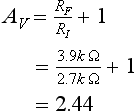
Output Voltage.
The output voltage of the circuit in Figure 2.25 can be determined by utilizing the basic gain equation of Equation (2.1):
2.6.3 Practical Design Techniques
The design of a noninverting summing amplifier like that shown in Figure 2.23 is an involved process, and the resulting design is difficult to alter without affecting several parameters. Therefore, many designers who need a noninverting summing amplifier utilize an inverting summing amplifier followed by a simple inverting amplifier. This arrangement is much simpler to design, easier to modify, and costs little more to build. With this in mind, we will not explore the details for designing the generic noninverting summing amplifier. However, we will discuss the design of a special case that uses the same basic circuit when we study adder circuits in Chapter 9.
2.7 AC-COUPLED AMPLIFIER
The term AC-coupled identifies the fact that only AC signals are allowed to pass through the amplifier. DC and very-low-frequency AC signals are blocked or at least severely attenuated. The concept of AC coupling is applicable to many amplifier configurations. In the following discussion, we will consider the operation of the basic inverting and noninverting amplifier circuits when they are configured to be AC coupled. Most of the operation, analyses, and design methods are similar to their DC-coupled equivalents, which have been covered in detail. Therefore, we will concentrate on areas that are unique to the AC-coupled circuit.
First let us examine the operation of the AC-coupled inverting amplifier circuit shown in Figure 2.26(a).

FIGURE 2.26 AC-coupled versions of the basic inverting amplifier (a) and the basic noninverting amplifier (b) circuits.
You will recall from basic electronics theory that a capacitor blocks DC and passes AC. More specifically, a capacitor’s opposition to current flow (capacitive reactance) increases as the applied frequency decreases. As the input frequency in Figure 2.26(a) decreases, the reactance of capacitors CI and CO both increase. As the reactance of CI increases, the combined impedance of CI and RI also increases. Since the voltage gain of the inverting amplifier is determined by the ratio of the feedback resistor to the input resistance, and since the input resistance (actually the combined impedance of CI and RI) is increasing, we know that the amplifier gain must be decreasing.
Another way to view the operation of the AC-coupled inverting amplifier is to consider that the output voltage of the amplifier is determined by the magnitude of feedback current. The feedback current that flows through RF is identical to that which flows through RI (ignoring the small bias current that flows in or out of the (−) input terminal). The value of current flow through RI is determined by the magnitude of the input voltage and the impedance of RI and CI in combination. As the frequency decreases toward DC, the input current, and therefore the feedback current, must decrease. This lowered feedback current causes a corresponding decrease in output voltage. Because the input voltage is constant but the output voltage is decreasing, we can conclude that the amplifier’s gain is dropping as the frequency is lowered.
The output capacitor CO also affects the frequency response of the circuit. Basically, the output resistance of the op amp, the load resistance, and CO form a series circuit across which the ideal output voltage is developed. That portion of the output voltage that appears across RL is the final or effective output voltage of the circuit. The remaining voltage that is dropped across the internal resistance and across CO is essentially lost. As the frequency in the circuit is decreased, the reactance of CO increases. This causes a greater percentage of the output voltage to be dropped across CO and leaves less to be developed across RL. Thus, the effects of CO also cause the frequency response to drop off on the low end and, in fact, prohibit the passage of DC signals.
Resistor RB helps compensate for the effects of op amp bias currents. Its value will generally be the same as that of the feedback resistor, since the input resistor (RI) is isolated by CI for DC purposes.
The AC-coupled noninverting amplifier circuit shown in Figure 2.26(b) is nearly identical to its direct-coupled counterpart, which we discussed in an earlier section. Coupling capacitors CI and CO allow AC signals to be coupled in and out of the amplifier. Very-low-frequency signals and DC in particular are not coupled through the capacitors and are therefore not allowed to pass through the amplifier. R1 and CI form an RC-coupling circuit on the input. That portion of the input signal that appears across R1 is actually amplified by the circuit.
2.7.2 Numerical Analysis
Most of the calculations for the basic direct-coupled inverting and noninverting amplifier circuits apply to the AC-coupled inverting and noninverting amplifier, respectively. For purposes of our present analyses, we will determine the following circuit parameters:
We will use the circuits shown in Figure 2.27 for our numerical analysis example.
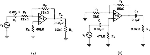
Voltage Gain.
We will compute the overall voltage gain of the inverting circuit, Figure 2.27(a), by considering the gain to be made up of two parts. The first part of the gain is determined by all components to the left of CO. The second part of the overall gain is determined by CO and RL. This latter part is actually a loss and tends to reduce the overall gain. Once these individual gains are computed, multiply them together to determine the overall voltage gain.
The voltage gain of the circuit to the left of CO is computed in basically the same way, Equation (2.6), as a direct-coupled inverting amplifier. That is,
The only modification to our original equation is that the denominator must also include the effects of CI. Therefore, instead of dividing by RI (as we did with the direct-coupled circuit), we simply divide by the net impedance of RI and CI (i.e., ZI). You will recall from basic electronics that the net impedance of a series RC circuit is computed with the following equation:
where XC is the capacitive reactance of CI. We already know that the gain of an op amp varies with frequency, but now we have introduced an even more obvious frequency-sensitive factor (XC). Thus, when we speak of voltage gain, we must refer to a specific frequency in order to have a meaningful discussion. In most cases, we are interested in the lowest input frequency because this is where the capacitors will have their greatest effect (i.e., gain will be the lowest).
For the portion of the circuit in Figure 2.27(a) left of CO, we can compute the voltage gain as shown. First, we need to determine the capacitive reactance with our basic electronics formula for XC.
For illustrative purposes, we will assume an input frequency of 800 hertz. The first step, then, is to calculate the reactance of CI at the frequency of interest.
Now we can compute the impedance of RI and CI:

Substituting this into the voltage gain equation, Equation (2.37), we can compute the gain of the circuit to the left of CO.
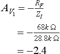
Recall that the minus sign indicates a phase inversion, but in no way implies a reduction in signal amplitude.
Our next step is to compute the effects of CO and RL. These two components form an RC voltage divider. You may apply your favorite circuit analysis method to determine the percentage of voltage that appears across RL. This percentage is the effective “gain” of the RC-coupling circuit. For our purposes, we will use the following method, which is based on the resistive voltage divider formula:
where Z is the net impedance of CO and RL.
First we compute the reactance of CO at the frequency of interest (800 hertz in this case):
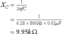
Next we compute the net impedance of RL and CO:

Finally, substituting this value into Equation (2.38), we compute our gain as

That is to say, about 97% of the signal amplitude that appears at the output terminal of the op amp will be developed across RL. The RC-coupling circuit appears to be working well at 800 hertz, since very little voltage is being lost across CO.
The overall voltage gain for the circuit is found by multiplying these two gains as computed.
For our example, we compute overall voltage gain as
Notice that the method described for computing overall voltage gain does not include the effects of the variations in open-loop gain at different frequencies. Although this additional consideration could be included as with the direct-coupled amplifier, it is not normally necessary because our calculations are accomplished at the lowest input frequency. If you want to compute the gain at some relatively high frequency, then you should include the effects of reduced op amp internal gain.
Another point that you may wish to consider involves phase shift. In addition to the 180-degree phase shift provided by the op amp itself, the signal also receives a phase shift from the two RC networks. The preceding calculations compute only the amplitude of the signal. If the phase is also an important consideration, then the same basic equations still apply but you can express the values as complex numbers. The final answer, then, not only will include the magnitude of the gain as computed, but will also reveal the amount of phase shift given to the signal.
The voltage gain calculation for the noninverting circuit shown in Figure 2.27(b) is similar, but will be considered as three separate gains that are multiplied together to find the overall gain. The three individual gains are
1. R1/CI network gain (actually a loss)
2. RL/CO network gain (actually a loss)
3. The gain of the op amp circuit as determined by RF and RI
The gains of the input and output RC circuits are computed in the same way that we computed the gain of the output RC circuit in Figure 2.27(a). Let us first calculate the input RC circuit gain. Our initial step is to compute the reactance of CI at the lowest frequency (assumed to be 800 hertz).

Next we find the net impedance of R1 and CI.

Finally we compute the voltage gain (loss) of the RC network with Equation (2.38).
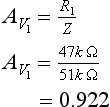
Similar calculations for the output RC network of Figure 2.27(b) can now be accomplished. First we find the reactance of CO.
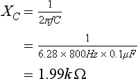
Next we compute the net impedance of RL and CO.

Finally, the effective voltage gain (loss) of the RLCO network can be computed, Equation (2.38).

The third portion of our overall gain calculation is the gain of the op amp circuit as determined by RF and RI. We compute this using the gain formula of Equation (2.28) presented for the direct coupled amplifier.
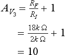
The effective overall gain at 800 hertz is found by multiplying the three individual gains, as in Equation (2.39).
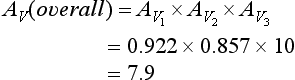
As with the AC-coupled inverting amplifier, we have chosen to ignore the frequency-dependent effects of open-loop op amp gain. This is generally a reasonable approach because our calculations are performed at the lowest input frequencies, where the open-loop gain is the closest to its ideal value.
Input Impedance.
The input impedance for the AC-coupled inverting amplifier circuit shown in Figure 2.27(a) is equal to the net impedance of RI and CI. Recall that the (−) input of the op amp is a virtual ground point. The source, therefore, sees the input impedance offered by CI and RI. Because this is a frequency-dependent value, we must discuss input impedance at a particular frequency of interest. For purposes of our present discussion, let us compute the highest and lowest values for input impedance if the input frequency range is 800 hertz to 3 kilohertz. The following input impedance at 800 hertz is computed. First we find the reactance of CI at 800 hertz.

Now we can compute the impedance of RI and CI.
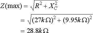
The minimum value for input impedance occurs at the highest input frequency. In most cases, the input impedance approaches the value of RI; however, the computations are similar to those as shown:

Now we can compute the impedance of RI and CI.

The input impedance for the AC-coupled noninverting amplifier circuit shown in Figure 2.27(b) is essentially equal to the impedance offered by R1 and CI. Technically, the input impedance of the (+) input terminal appears in parallel with R1. We can generally ignore this impedance, however, since it is usually an extremely high value. For our present example, we begin by finding the reactance of CI at the lowest input frequency.
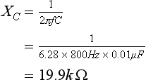
Next we find the net impedance of R1 and CI.
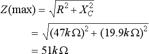
The minimum value for input impedance occurs at the highest input frequency, as it did with the inverting circuit. In most cases, the input impedance approaches the value of R1. The following computations, however, are shown:

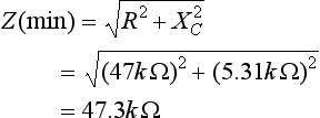
Bandwidth.
Bandwidth can be defined as that range of frequencies that pass through a circuit with a voltage amplitude of at least 70.7 percent of the maximum output voltage—in other words, the range of frequencies between the two half-power points. These two frequencies can be readily determined in at least three ways:
You may be able to employ all three of these methods. However, none of them are suitable for use in this reference book, so we will examine yet another, less direct approach. Let us begin by making some observations. First, since the op amp has a frequency response that extends all the way to DC, the lower cutoff frequency will be unaffected by the op amp. That is, the input and output RC circuits will determine the lower cutoff frequency. Second, in a practical circuit, the upper cutoff frequency will be determined by the op amp itself. The RC circuits act as high-pass filters and will not restrict the gain at the higher input frequencies.
Calculation of the upper cutoff frequency was discussed in previous sections. We estimate it with Equation (2.40).
In the case of Figure 2.27(a), our ideal upper cutoff frequency is computed as
Next we calculate the lower cutoff frequency, which is determined by the input and output RC networks. The cutoff frequency of each individual RC network is determined with the following equation:
The lower cutoff frequency for the entire circuit is determined by the ratio of the cutoff frequencies for the RC circuits.
Let us now compute the lower cutoff frequency for the circuit in Figure 2.27(a). First we compute the individual cutoff frequencies for the two RC networks. The input circuit calculations, as in Equation (2.41), are
A similar computation, Equation (2.41), for the output RC circuit is
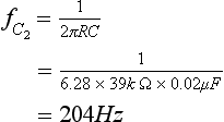
Computing the ratio of the two cutoff frequencies (using the higher frequency as the numerator) gives us the index needed for the lookup operation in Table 2.5.

For our particular case, the index is computed as
Finally, we use the lookup table shown in Table 2.5 to get our multiplying factor k. In this case, the value of k is about 1.32 (estimating the value between 1.34 and 1.306). The overall lower cutoff frequency can now be found by multiplying our factor k by the higher of the two individual cutoff frequencies.
Thus, the lower cutoff frequency for the circuit in Figure 2.27(a) is estimated as
The approximate bandwidth of the circuit in Figure 2.27(a) can now be expressed as Equation (2.5):
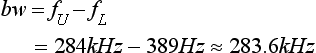
The bandwidth of the noninverting circuit shown in Figure 2.27(b) is computed in the same way that it was for the inverting circuit. First we estimate the upper cutoff frequency, which is determined by the behavior of the op amp, from Equation (2.22).
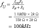
Next we compute the individual cutoff frequencies for the input and output RC circuits, as in Equation (2.41).
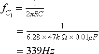
A similar computation for the output RC circuit is Equation (2.41):

Computing the ratio of the two cutoff frequencies (using the higher frequency as the numerator) gives us the index, from Equation (2.42), needed for the lookup operation in Table 2.5:
Using this value as the index into Table 2.5 gives us an approximate value of 1.33 for k. The lower cutoff frequency for the entire circuit in Figure 2.27(b) can now be estimated with Equation (2.43):
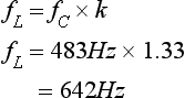
At this point, the bandwidth of the circuit can be estimated with Equation (2.5):
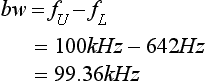
2.7.3 Practical Design Techniques
The design of either the inverting or the noninverting AC-coupled amplifier is a relatively easy process. Following are the sequential steps:
1. Design the basic amplifier circuit according to the guidelines presented for the direct-coupled inverting or noninverting amplifier circuits.
2. Compute the values for the input and output RC coupling components.
As an example, let us design a noninverting AC-coupled amplifier that has the following characteristics:
1. Midpoint voltage gain of 12
2. Lower cutoff frequency of 500 hertz
Determine the Value of RI.
We will select RI as 6.8 kilohms. Although this selection is somewhat arbitrary, we are keeping within the guidelines of choosing resistance between 1000 ohms and 680 kilohms. Additionally, the selection of RI will have a major effect on the final input impedance, as R1 will be close to the same value as RI, and it is R1 that determines the input impedance of the amplifier. Thus, in order to meet the requirements for an input impedance of at least 3000 ohms, we must choose a value for RI that is larger than 3000 ohms.
Determine the Value of RF.
RF can be computed from the voltage gain equation shown in Equation (2.28):

For the present design example, we compute RF as follows:
We select the nearest standard value of 75 kilohms to use as RF.
Determine the Required Unity Gain Frequency.
We can compute the minimum unity gain frequency for our op amp with Equation (2.22):
where fUG is the minimum required unity gain frequency for the op amp and bw is the highest operating frequency. Thus, we must select an op amp that has a minimum unity gain frequency of at least 180 kilohertz. Because the 741 has a 1.0-megahertz unity gain frequency, it should be fine for our purposes. Now let us determine the slew-rate requirement.
Determine the Required Slew Rate.
The minimum acceptable slew rate for the op amp is given by the following equation, Equation (2.11):
In our case, let us assume that we want to deliver a full output swing (±13 V) at the highest frequency (15 kHz). The minimum slew rate is computed as follows:
The 741 has a slew rate of 0.5 volts per microsecond, so it will not be adequate for this application. There are many alternatives, but let us choose the MC1741SC op amp (Appendix 4). It has a unity gain frequency similar to that of the 741, but it offers a slew rate of 10 volts per microsecond.
Select R1.
R1 is chosen to be the same value as the parallel combination of the feedback resistor (RF) and the input resistor (RI). This following value is computed:

Compute the Value of CI.
To simplify subsequent calculations, we will choose a value for CI that produces a reactance that is much less than the resistance R1. We will design for a reactance of one-tenth R1, or 620 ohms in this case, at the lower cutoff frequency. The value for CI is computed from the capacitive reactance equation.
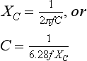
We will select the next higher standard value of 0.56 microfarad.
Select the Value of RL.
In many cases, RL is the input resistance of a subsequent stage. In these cases, RL is not selected; it is already defined by the nature of the problem. For our example design, we will choose RL as 27 kilohms. This is sufficiently large to eliminate any concerns of output loading on the op amp, but it is low enough to facilitate coupling to a subsequent op amp circuit if needed.
Compute the Value of CO.
By following the guidelines given for the selection of the R1CI combination, we have assured ourselves that the lower cutoff frequency will be primarily determined by the RLCO network. We use the fundamental formula for capacitive reactance to compute a value for CO that produces a reactance equal to the value of RL at the lower cutoff frequency (500 Hz).
The resulting circuit for our noninverting AC-coupled amplifier is shown in Figure 2.28. The actual performance of the circuit is reflected in the oscilloscope waveforms shown in Figure 2.29. The design goals are compared to the measured performance in Table 2.6.
TABLE 2.6
| Parameter | Design Goal | Measured Values |
| Midpoint voltage gain | 12 | 11.9 |
| Frequency range | 500 Hz–15 kHz | 475 Hz–79.5 kHz |
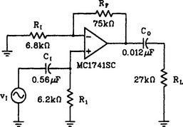
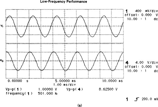
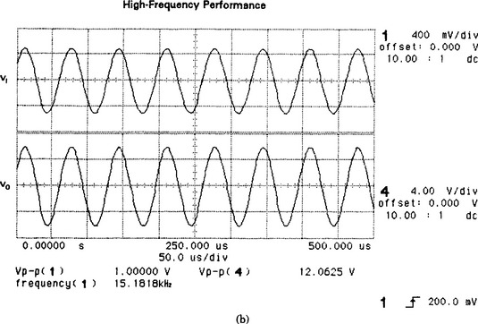
FIGURE 2.29 Oscilloscope displays showing the actual performance of the AC-coupled amplifier shown in Figure 2.28. (Test equipment courtesy of Hewlett-Packard Company.)
2.8 CURRENT AMPLIFIER
Figure 2.30 shows the schematic diagram of a basic current amplifier. This circuit, as its name implies, accepts a current source as its input and delivers an amplified version of that current to the load. The load, in the case of Figure 2.30, is not directly referenced to ground. A current source is normally designed to drive into a very low (ideally 0) impedance. In the case of the circuit in Figure 2.30, the (−) input of the op amp is a virtual ground point. Thus, the current source sees a very low input resistance.

All of the current that leaves the source must flow through resistor R2, since we know that no current flows in or out of the op amp input (except for bias current). The current flowing through R2 produces a voltage drop that is determined by the value of R2 (a constant) and the value of the input current. Once the circuit has been designed, the voltage drop across R2 is strictly determined by the amount of input current (iI). Notice that resistors R2 and R1 are essentially in parallel, because R2 is connected to a virtual ground point. Because the two resistors are in parallel, we know that the voltage across them must be the same. That is, the voltage across R1 will be the same as the voltage across R2 and is determined by the value of input current. The current through R1 can be determined by Ohm’s Law. If the value of R1 is smaller than the value of R2 (the normal case), then current i1 will be proportionally larger than iI, (recalling that the voltages across the parallel resistors are equal).
Kirchhoff’s Current Law would show us that the current iI and i1 must combine to produce the load current iL. The value of iL is strictly determined by the input current, but its value will be larger by the amount of current (i1) flowing through R1. Thus, we have current gain or current amplification. The larger we make i1 as compared to iI, the higher the current amplification. Examination of the circuit will confirm that the circuit can accept current of either polarity as long as the op amp is operating from a dual power supply.
2.8.2 Numerical Analysis
Now analyze the current amplifier shown in Figure 2.30, and compute the following values:
Current Gain.
The current gain (AI) can be initially described with the basic gain equation, Equation (2.1):
Current iL is composed of the two currents, i1 and iI. That is,
The voltage across R1 is equal to the voltage across R2 and is computed by Ohm’s Law as
The value of current (i1) can also be computed by Ohm’s Law as
Substituting this into the equation for load current produces
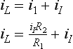
Factoring iI, gives us the equation for IL:
In this form, it is easy to see that we do indeed have a current amplifier. That is, the input current (iI) is multiplied by a constant (R2/R1 + 1) to produce the output or load current. The constant is the current gain of the circuit, shown below.
In the case of the circuit in Figure 2.30, the current gain is calculated as shown:
It is especially important to note that the value of load current is independent of the value of load resistor. That is, the op amp circuit is acting as a current source.
Although many current sources are essentially DC (e.g., transducers), there may be an application requiring current amplification at higher frequencies. As the frequency of operation is increased, the actual current gain will begin to decrease from the low frequency value calculated. This effect is caused by the reduction in open-loop op amp gain as the input frequency is increased. The higher the value of current gain (AI), the more significant the effects of op amp voltage gain variations.
Load Current.
The input current (iI) for the circuit in Figure 2.30 is indicated to be in the range of 10–50 microamps. The output current can be found by transposing the basic current gain equation, Equation (2.1).

In our case, the minimum load current is computed as
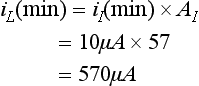
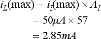
Range of Acceptable Input Currents.
In order for the circuit in Figure 2.30 to operate as a current source whose value is proportional to input current, it is essential that the output voltage (vO) be less than the saturation voltage in either polarity. This, then, is the factor that restricts the range of acceptable input currents. The output voltage can be expressed as a sum of two voltages by using Kirchhoff’s Voltage Law.
Substituting current and resistance values (i.e., V = IR) produces
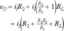
To calculate the amount of input current needed to drive the output to saturation, we transpose this equation to find iI and substitute the value of VSAT for vO. For our example, let us assume that the saturation voltage is determined from the manufacturer’s data sheet to be 13 volts. The maximum input current, then, is computed as
More specifically, for our present circuit we have
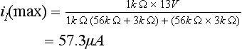
The lower range is computed in a similar manner by using the other saturation limit. In most cases (i.e., balanced dual power supply circuits), the values of ±VSAT will be the same. If this were true for the circuit in Figure 2.30, we could have a range of input currents that extended from -57.3 microamps to +57.3 microamps—the polarity, of course, telling us the direction of current flow.
Maximum Load Resistance.
Another way to view the preceding calculations is to consider a known range of input currents and a variable value for RL. Again, the output voltage must be kept from reaching the saturation limits. We can transpose Equation (2.46) for iI(maximum) to get the following result:
where iI is the highest expected input current. In the case of Figure 2.30, we can determine the maximum value for the load resistance as
Input Resistance.
Although the input resistance of the circuit in Figure 2.30 is ideally 0, there may be applications that require us to know a more accurate value for it. The following equation can be used to estimate the input resistance of the current amplifier in Figure 2.30:
where RX is the resistance of R1 and R2 in parallel (i.e., R1R2/(R1 + R2)) and AV is the open-loop gain of the op amp at a particular frequency.
In the case of Figure 2.30, let us compute the input resistance for DC conditions. First, the open-loop gain at DC can be found in the data sheet (Appendix 1) to be at least 50,000. The value for RX is calculated as

The input resistance can now be calculated, Equation (2.47), as shown:
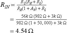
As you might expect, the input resistance approaches the ideal value (to be driven by a current source) of 0 ohms.
If the input frequency is higher than DC, the input resistance will deviate more from the ideal value of 0. For example, if our input frequency were raised to 1 kilohertz, the input resistance would increase to about 226 ohms. Additionally, we would need to consider the effects of bandwidth and slew rate limitations.
Output Resistance.
The output resistance of the circuit in Figure 2.30 as viewed by the load resistor is ideally infinite, as the circuit acts like a current source. A more accurate value for the output resistance can be computed with the following equation:
where AV is the open-loop voltage gain of the op amp at a particular frequency and RX is the value of R1 and R2 in parallel. In the case of Figure 2.30, let us estimate the output resistance at DC:
As evidenced in the equation, this value becomes less ideal as the frequency of operation is increased.
2.8.3 Practical Design Techniques
A practical current amplifier circuit can be designed by applying the equations discussed in the preceding paragraphs. Depending on the application, you will know some combination of the following parameters:
For purposes of a design example, let us build a current amplifier that satisfies the following requirements:
1. Output current of 10 milliamps (constant)
2. Input current of 500 microamps
3. Load resistance of < 500 ohms
Compute the Required Current Gain.
The required current gain of our circuit can be computed with the basic current gain equation, Equation (2.1):
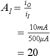
Determine the Maximum Value for R2.
The maximum value for R2 can be found by applying a transposed version of the equation we used for computing the maximum value for RL:

We will select a standard value less than this–for purposes of our design, a 12-kilohm resistor for R2. Notice that we use the worst-case value of 12 volts as the saturation voltage for the op amp.
Compute the Value of R1.
R1 can be computed by applying a transposed version of the current gain equation, Equation (2.45).
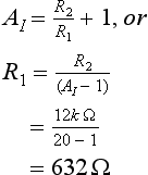
We will select the nearest standard value of 620 ohms. If it is essential to have a precise value of load current, then we put a variable resistance in series with R2.
The schematic of our completed design is shown in Figure 2.31. The load resistor has been replaced with a zener diode to illustrate a possible application. By forcing the zener current to be a known value, we can measure the zener voltage and compute the zener resistance. As long as the effective zener resistance is below our established limit for RL, the circuit will work fine. The measured performance of the circuit is contrasted with the design goals in Table 2.7.
TABLE 2.7
| Parameter | Design Goal | Measured Values |
| Input current | 500 μA | 500 μA |
| Output current | 10 mA | 9.97 mA |
| Current gain | 20 | 19.9 |
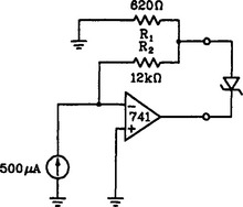
2.9 HIGH-CURRENT AMPLIFIER
A general-purpose op amp can supply only a few milliamps to a load. The 741, for instance, has a short-circuit output current of 20 milliamps. Some applications require substantially higher currents. The circuit in Figure 2.32 illustrates one common method for increasing the available current at the output of an op amp circuit. This technique is illustrated for a simple inverting amplifier, but is applicable to most voltage amplifier circuits.
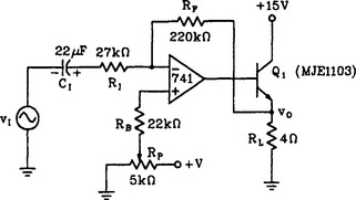
The bulk of the circuit operation is identical to that discussed with reference to the basic inverting amplifier circuit and will not be repeated here. Recall that resistors RF and RI determine the voltage gain of the circuit. Resistor RB is to compensate for op amp bias currents. Potentiometer RP has been added to the basic inverting amplifier and will be used to force an offset in the output.
The output voltage of the op amp appears on the base of Q1. A similar voltage appears on the emitter of Q1, which is connected as a voltage follower. The actual voltage on the emitter is less than the base voltage by a small amount (≈0.7 volts). In general, the output voltage across RL is essentially the same as the output voltage of the op amp. The output current of the op amp provides base current to the transistor. The load current, on the other hand, is provided by the transistor’s emitter current. You will recall that the transistor emitter current and the base current are related by a current gain factor called β or hFE, which can range from about twenty up to several thousand. With the circuit connected as shown, the load can draw β times as much current as the basic op amp supplies.
In order for the circuit to operate properly, the base voltage on Q1 must always be positive with reference to ground, since the load is returned to ground. Ordinarily, an AC signal applied to a split-supply op amp would produce bipolar signals on its output. To prevent this situation, we adjust RP to establish a positive bias on the base of Q1 that is approximately equal to half of the positive saturation voltage. The output signal can then swing from near 0 up to near saturation. Recognize that this swing is only half of the swing available with previous amplifiers and represents a disadvantage of the circuit shown in Figure 2.32. An alternative is to return the load to the negative 15-volt supply (emitter bias).
One very important characteristic of the circuit in Figure 2.32 is that output voltage is unaffected by changes in VBE. We know VBE is approximately 0.7 volts for silicon transistors, but we also know it changes with temperature and varies from one transistor to another. By connecting the feedback resistor (RF) to the emitter rather than directly to the output of the op amp, we include the base-emitter junction in the feedback circuit. Changes in the base-emitter voltage are now effectively compensated by the op amp.
Since the (+) input on the op amp is at some positive level, the (−) pin will also be at a similar level. If the input signal were centered on 0 volts, this could cause an undesired DC offset in the output. Capacitor CI is included to isolate the DC level on the (−) pin from the DC level associated with the signal source. If it is sufficiently large, it has no effect on the gain calculations in the circuit. If its reactance at the lowest input frequency exceeds one-tenth the resistance of RI, then the gain of the circuit should be computed in the same manner as the AC-coupled amplifiers discussed in a previous section.
2.9.2 Numerical Analysis
Let us now numerically analyze the behavior of the circuit shown in Figure 2.32. Appendix 1 shows the data sheet for the 741 op amp, and Appendix 2 shows the specifications for an MJE1103 transistor. First, we know from our basic transistor theory that the impedance looking into the base will be approximately equal to β times the resistance in the emitter circuit. Thus, the op amp sees the load resistance as
In the case of Figure 2.32, the emitter resistance appears as
We can now refer to the 741 data sheet and determine the worst-case saturation voltage when using a ±15-volt supply and driving a 3000-ohm load. This value is listed as 10 volts.
The transistor data sheet indicates that the base-emitter voltage drop is 2.5 volts or less. Thus, the highest (worst-case) voltage that we can expect at the load is
For the circuit in Figure 2.32, we have
The unusually high value of VBE stems from the fact that the MJE1103 is a high-current Darlington pair. With Ohm’s Law, we can calculate the maximum instantaneous (i.e., peak) load current as

The op amp must supply a current that is smaller than load current by a factor of β. That is,
In our case, the calculations are
This current is well within the range of op amp output currents, even though the load current itself is nearly two amps.
In order to ensure that we have a maximum symmetrical swing for the output signal, we will establish a positive DC offset in the output. The value of this offset should be midway between the two extremes. One extreme is the value of VSAT, or +10 volts. The other extreme is the minimum turn-on voltage for Q1 and is 2.5 volts. The DC level on the output of the op amp must then be
The maximum voltage swing at the output of the op amp will be

We will get this same swing at the load, but the DC level will be reduced by the amount of VBE.
If the output of the op amp is allowed to go more positive than +VSAT (estimated here as +10 volts), the waveform will be clipped on its positive peaks. This clipped waveform will also appear across the load.
If the output of the op amp is allowed to go below the minimum turn-on voltage for Q1 (estimated here as +2.5 volts), the waveform will be clipped on its negative peaks. The load voltage will also have a clipped waveform.
If the amplitude of the input signal remains fixed, but the DC offset voltage in the output of the op amp is changed, then similar waveform clipping can occur. That is, if the instantaneous value of the combined AC and DC voltages on the output of the op amp goes more positive than +VSAT or less positive than the turn-on voltage for Q1, the output waveform will be distorted.
The sketch in Figure 2.33 clarifies the relationships between the output waveforms (op amp and load), the bias level, and the clipping levels.
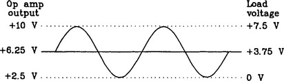
In order to establish the 6.25-volt DC bias at the output of the op amp, we need to adjust potentiometer RP to the necessary level. Although this would have to be done in a lab environment, we can compute the required value of voltage at the (+) input of the op amp. Since capacitor CI acts as an open to DC, the op amp is essentially configured as a voltage follower with reference to the DC offset voltage at potentiometer RP. Therefore, to obtain a 6.25-volt offset in the output, we will need a 6.25-volt offset on the noninverting (+) input of the op amp.
We have already determined that the maximum output voltage swing is 7.5-volts peak-to-peak. We can determine the maximum input swing before distortion by applying the voltage gain formula, Equation (2.6), for an inverting amplifier.
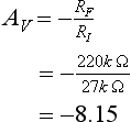
This can now be used with the basic voltage gain equation, Equation (2.1), to compute the maximum allowable input swing.

This can be more conveniently discussed as an RMS value, so we will convert it using our basic electronics conversion factor:
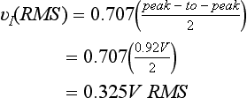
If we drive the amplifier with a signal greater than 0.325 volts RMS, we can expect clipping to occur in the output.
The input impedance of the circuit is approximately equal to the value of RI. We can apply Ohm’s Law to compute the current supplied by the AC input source under maximum input voltage conditions.
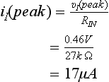
The usefulness of the circuit should become very apparent after this last calculation. A signal source delivering a peak current of 17 microamps is driving a load resistance that requires 1.88 amps peak current.
2.9.3 Practical Design Techniques
Much of the design procedure was covered in our numerical analysis discussion in the preceding section. Let us now design a high-current amplifier that will perform according to the following:
1. Input voltage of 1.0 volt RMS
2. Input resistance > 10 kilohms
3. Input frequency range between 10 hertz and 2.0 kilohertz
Select the Output Transistor.
There are basically five transistor parameters that must be reviewed to select a transistor:
1. Forward current transfer ratio (hFE) or current gain (β)
2. Base-emitter voltage drop (VBE)
In some cases, the frequency characteristics of the transistor must be evaluated, but in most cases the transistor performance exceeds that of the op amp and can be ignored.
In our case, we need an emitter-collector breakdown voltage greater than 15 volts. The exact collector current will be computed later, but we need to estimate a worst-case value so that we can select the transistor. For this purpose, we can assume that the entire +15 volts of the supply are felt across the 50-ohm load. Ohm’s Law tells us the value of load current.
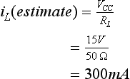
The actual collector current will be less than this, but this is a good value to use for initial transistor selection.
Now we need to determine the required current gain (β) of the transistor. In data sheets, this is generally labeled as hFE. We can again make a rough estimate for purposes of transistor selection. If we divide the load current computed above by half of the short-circuit output current of the op amp, we will have a good place to start. The following computation gives us the minimum value of β that our transistor should have.
The short-circuit current for a 741 is listed as 20 milliamps, and so in the present case we have
The power dissipation of the transistor can be estimated with the following equation:
where VCC is the positive supply voltage. For the present case, the estimated power dissipation of the transistor is
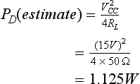
By scanning a transistor data book (selector guides in particular), a transistor that satisfies the above requirements can be found. For illustration purposes, let us select a 2N3440 transistor. The data sheet for this common device is presented as Appendix 9. Its critical parameters follow:
| 1.β or hFE | 160 |
| 2.Base-emitter voltage drop (VBE) | 1.3 volts (maximum) |
| 3.Emitter-collector breakdown voltage | 250 volts (minimum) |
| 4.Maximum collector current | 1.0 amps |
| 5.Power dissipation | 10 watts |
| 6.Thermal resistance, junction to case (θJC) | 17.5°C/W |
| 7.Thermal resistance, junction to air (θJA) | 175°C/W |
| 8.Maximum junction temperature | 200°C |
These values exceed our rough, worst-case requirements. Now let us extend our estimate to include the determination of a heat sink (see Appendix 10 for a more complete discussion). We will assume that 50°C will be the highest expected ambient temperature. The required thermal resistance (θJA) can be estimated as follows:
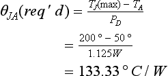
Since the required value of θJA is greater than the transistor’s θJC, this transistor can be used for this application. However, since the required value of thermal resistance (θJA) is less than the θJA for the transistor, a heat sink will be needed to ensure safe operation. The required thermal resistance (θSA) of the heat sink can be estimated as follows:
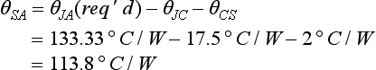
Note that the case-to-sink thermal resistance (θCS) was estimated as 2°C/W. Since the required thermal resistance is only slightly lower than the transistor’s own thermal rating, it should be easy to find or make a satisfactory heat sink. There are many transistor/heat sink combinations that are adequate for a given application. Final selection must include cost and availability considerations.
Determine the Maximum Output Voltage of the Op Amp.
The maximum op amp output voltage is simply VSAT. Appendix 1 lists the data sheet for a 741. The worst-case saturation voltage is listed as 10 volts for resistive loads of 2 to 10 kilohms. If the load on the op amp is over 10 kilohms, the saturation voltage is listed as 12 volts minimum. The load as seen by our op amp is computed by applying a basic transistor equation, Equation (2.49).

Thus, the maximum available voltage at the output of the op amp will be considered to be 10 volts. In practice, it will likely be higher.
Determine the Minimum Output Voltage of the Op Amp.
The lower limit on op amp output voltage is determined by the VBE value of the transistor. The worst-case value for the 2N3440A is given as 1.3 volts. Thus, our op amp output voltage can swing as low as 1.3 volts without fear of clipping.
Determine the Required Bias Voltage at the Output.
The output of the op amp should be biased halfway between its two limits (VSAT and VBE). This is computed as shown using Equation (2.52):
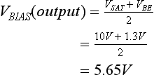
Determine the Maximum AC Swing at the Output.
The output of the op amp is centered at the bias level and can swing between VSAT and VBE. The RMS value of output voltage is computed as
Compute the Required Voltage Gain.
The required voltage gain of the amplifier circuit is determined by applying the basic voltage gain equation, Equation (2.1).
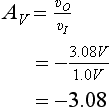
Determine the Value of RI.
The value of the input resistor is chosen to establish the required input resistance of the circuit. In our case, anything greater than 10 kilohms should suffice. Let us choose a standard value of 18 kilohms.
Calculate the Value of RF.
RF is calculated with the inverting amplifier gain equation, Equation (2.6).
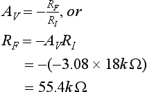
Determine the Required Unity Gain Frequency.
The required unity gain frequency is computed in a manner similar to that in previous discussions, using Equation (2.22).
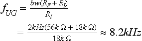
Select a Value for RP.
The value of the potentiometer RP is essentially arbitrary. As it is made smaller, its power rating requirement becomes higher, and the current draw from the supply becomes greater. If RP is made excessively large, then the effects of bias currents that flow through RP are more pronounced. As a guideline, select RP to be approximately equal to RF/10, but consider 1.0 kilohm to be the minimum practical value. In our case, we have
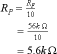
Compute the Value of RB.
The optimum value for RB varies as the wiper arm of RP is moved. However, the preceding method for selecting RP reduces this dependency. We will compute the value of RB needed when the wiper arm of RP is at midpoint. RB is computed as shown.
Compute the Value of CI.
The purpose of the input coupling capacitor is to isolate the DC levels between the signal source and the (−) pin on the op amp. It should be selected to have a reactance of less than one-tenth of RI at the lowest input frequency (10 hertz in this case). The calculations are
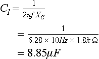
Bandwidth and Slew Rate Considerations.
Since our application requires only modest performance, neither slew rate nor bandwidth limitations should pose problems. If the application were more demanding, these restrictions would have to be considered. The methods described for previous amplifier circuits can be utilized to evaluate the effects of bandwidth and slew rate limitations.
The schematic of our completed design is shown in Figure 2.34. Actual performance of the circuit is indicated by the oscilloscope display shown in Figure 2.35.


FIGURE 2.35 Oscilloscope displays showing the actual performance of the high-current amplifier shown in Figure 2.34. (Test equipment courtesy of Hewlett-Packard Company.)
2.10 TROUBLESHOOTING TIPS FOR AMPLIFIER CIRCUITS
In order for an amplifier to operate properly, it must be biased in its linear range of operation. That is, the output must be between the two saturation limits with no signal applied. Many, if not most, of the problems encountered when troubleshooting op amps configured as linear amplifiers result in the output being driven to one of the saturation limits. Your task, then, is to recognize the symptoms and to locate the defective component.
If the amplifier circuit is properly designed (i.e., capable of achieving the desired performance), you can generally diagnose the problem by comparing the actual to ideal op amp behavior. The following are two critical characteristics to remember when troubleshooting amplifier circuits utilizing op amps:
1. The output should be between the saturation limits.
2. The differential input voltage (vD) should be very near 0.
2.10.1 Basic Troubleshooting Concepts
When troubleshooting any type of circuit, it is important to use a logical, systematic technique. Although there are several accepted methods, the following sequence of activities is a common and effective procedure:
Observation.
This is probably the most important step in the process if done effectively. Observation means more than just looking at the circuit. It includes all of the following actions:
1. Interrogate the owner, user, or operator for clues regarding how the trouble developed.
2. Operate the user controls and observe the behavior for clues.
3. Use your senses. Do you see any visible damage? Do you smell burned components? Do you hear suspicious sounds?
4. Be alert to similarities between observable symptoms on the defective unit and the symptoms of previously diagnosed circuits.
Many problems can be identified during the observation stage. How many of us have “successfully” traced a malfunction throughout a complex circuit until we located a suspected switch or variable resistor on the schematic? Then, when we physically locate the suspected component on the system, it turns out to be a front panel control! Had we applied the preceding procedure faithfully, we could have reduced our efforts dramatically.
Signal Injection/Tracing.
All electronic circuits can be diagnosed to some extent by signal injection, signal tracing, or a combination of the two methods. The underlying goal for this process is to reduce the number of possible culprits down from a set consisting of every component in the system to a smaller set consisting of only a few components.
Signal injection requires us to inject a known, good signal at some point in the circuit and observe the effects. If the circuits that utilize this signal then appear to operate normally, we can infer that the malfunction is located ahead of our injection point. We then move our injection point closer to the source of the trouble and inject another signal. Again, the behavior of the subsequent circuits will provide guidance as to our next injection point. Two common types of test equipment for signal injection are signal generators and logic pulsers.
Signal tracing is similar in concept, except we put a known good signal at the input and verify (trace) its presence throughout the circuit. If we lose the signal (or it becomes distorted) at a certain point, then we can infer that the trouble lies ahead of the monitored point. The oscilloscope and logic probe are two common types of signal tracing equipment.
Both signal tracing and signal injection can be enhanced by using the split-half method of troubleshooting. By selecting your injection or monitor point to be approximately halfway through the suspected range of components, each measurement effectively reduces the number of possible components by half.
Voltage Measurements.
Voltage measurements normally occur after you have isolated the problem down to a particular stage consisting of up to perhaps 10 components. The voltage checks contrasted with normal values should result in the narrowing of suspects down to one or two possibilities. Distinction between the signal tracing and voltage measuring phases often becomes blurred when an oscilloscope is used. The concept remains valid, however.
Resistance Measurements.
Resistance checks are performed last because accurate measurements often require desoldering of a component. Desoldering not only is time consuming but also risks damage to an expensive printed circuit board in many cases. The resistance checks are done to verify that you have in fact located the defective component. Component testers can also be used at this point if available and appropriate.
2.10.2 Specific Techniques for Op Amps
Through observation and signal injection/tracing, the technician can normally isolate the problem down to a specific circuit. For this discussion, we will assume the problem has been isolated to an amplifier circuit built around an op amp. The following sequence of activities will normally isolate the defective component:
1. Verify the power supply voltage on the op amp.
3. Measure differential input voltage (vD).
4. Compare the results of steps 2 and 3. If the results violate basic theory (e.g., noninverting input is more positive than inverting input, but output is negative), then the op amp is probably bad. If no basic theory principles are violated, check the following:
Your most powerful troubleshooting tool when diagnosing op amp circuits is a solid grasp of the basic theory of operation. Although the performance of op amps can deteriorate in some ways, it is far more common for the device to exhibit catastrophic failure.
REVIEW QUESTIONS
1. A certain amplifier has a voltage gain of 100. Express this gain in decibels.
2. Suppose the amplifier circuit shown in Figure 2.3 is altered to have the following values:
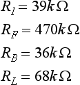
What is the voltage gain of the circuit with the new values? What happens to the voltage gain if RL is decreased to 27 kilohms?
3. Refer to the amplifier circuit described in question 2. Compute the input impedance of the circuit. Does the input impedance change if RL is reduced to 27 kilohms?
4. If a 741 op amp is powered by a ±15-volt supply, what is the largest voltage swing that can be guaranteed on the output if the load is 18 kilohms? Repeat this question for a 2.0-kilohm load.
5. A certain op amp application requires a 5-volt RMS output voltage swing and operates at a maximum sinewave frequency of 21.5 kilohertz. What is the minimum slew rate for the op amp that will allow the signal to pass without substantial slew rate distortion?
6. A simple noninverting amplifier (similar to Figure 2.12) has the following component values:
| Op amp | 741 |
| RI | 4.7 kΩ |
| RF | 68 kΩ |
| RL | 18 kΩ |
| RB | 4.3 kΩ |
Compute the small signal bandwidth of the amplifier (ignore slew rate considerations).
7. The value of CI in Figure 2.26(a) is the primary factor that sets the upper cutoff frequency. (True or False) Explain why or why not.
8. If capacitor CO in Figure 2.26(b) becomes open, what effect will this have on circuit operation to the left of capacitor CO?
9. If capacitor CI in Figure 2.26(b) becomes open, what happens to the DC voltage on the output pin of the op amp? What happens to the DC voltage across RL?
10. Refer to Figure 2.32. As the wiper arm of RP is moved to the right, what happens to the average current through RL?
11. Refer to Figure 2.32. If the wiper arm of RP is moved too far to the left, the output waveform will start to clip. Explain which peak (positive or negative) is clipped and why.
12. Refer to Figure 2.21. What happens to the average (i.e., DC) current through RL if RI1 becomes open?
13. What is another name for a noninverting amplifier with a voltage gain of 1?
14. Can a standard 741 op amp be used to amplify a 33-kilohertz signal if the desired voltage gain is 5 and the maximum peak output voltage swing is 11 volts? Explain your answer.
15. While troubleshooting the circuit shown in Figure 2.27(a), you discover that the voltage on the inverting (−) pin of the op amp is approximately 0 volts (with a normal signal applied at the input). If you think this is normal, explain why. If you think it is abnormal, what is the most likely defect?