Arithmetic Function Circuits
This chapter presents several circuits designed to perform mathematical operations, including adding, subtracting, averaging, absolute value, and sign changing. Several other common but more complex circuits that perform mathematical functions are presented in Chapter 11.
9.1 ADDER
An adder circuit has two or more signal inputs, either AC or DC, and a single output. The magnitude and polarity of the output at any given time is the algebraic sum of the various inputs. In Chapter 2, we discussed an inverting adder circuit, called an inverting summing amplifier. If we make the feedback resistor and all input resistors the same size, the circuit provides a mathematically correct sum (i.e., no voltage gain). The following discussion will introduce the noninverting adder circuit.
9.1.1 Operation
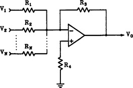
Figure 9.1 shows the schematic diagram for a noninverting adder circuit. The input signals may be AC, DC, or some combination. The op amp, in conjunction with R1 and R2, is a simple noninverting amplifier whose gain is determined by the ratio of R2 to R1. Whatever voltage appears on the (+) input will be amplified.
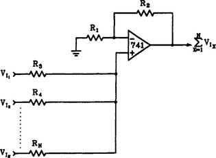
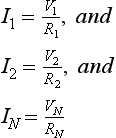
The voltage that appears on the (+) input is the output of a resistive network composed of R3 through RN and the associated input voltages. Since all input resistors are equal in value and connect together at the (+) input, we can infer that the relative effects of the inputs are identical. The absolute effect, of course, is determined by the gain of the amplifier. If R2 is set to the correct value, then the gain of the op amp will be such that the output voltage corresponds to the sum of the input voltages.
9.1.2 Numerical Analysis
We will now analyze the circuit shown in Figure 9.2 to numerically confirm its operation. Let us first determine the behavior of the op amp and its gain resistors (R1 and R2). These components form a standard noninverting amplifier whose gain can be determined with the familiar gain equation.
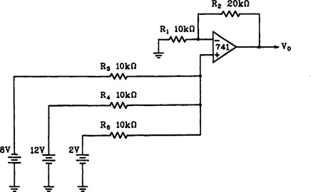
The voltage gain of a noninverting adder will always be the same as the number of inputs.
All that remains is to determine the value of voltage on the (+) input pin. One method for calculating this voltage is to apply Thevenin’s Theorem to the network, which will give us an equivalent circuit consisting of a single resistor and a single voltage source. The application of Thevenin’s Theorem is shown sequentially in Figures 9.3(a) through 9.3(c). Figure 9.3(a) shows the original input network. We will apply Thevenin’s Theorem to the portion of the circuit within the dotted box.

FIGURE 9.3 Application of Thevenin’s Theorem to simplify the input network of the noninverting adder circuit.
First we see that we have two opposing voltage sources in this part of the circuit that yield a net voltage of
Now, with two equal resistors in the circuit, there will be 5 volts dropped across each one. The equivalent Thevenin voltage, then, can be found with Kirchhoff’s Voltage Law.
Alternately, we could apply Kirchhoff’s Voltage Law as
By replacing the two sources with their internal resistances (assumed to be 0), we can determine the Thevenin resistance, which is simply the value of R5 and R4 in parallel.
The results of our first simplification are shown in Figure 9.3(b). The Thevenin equivalents computed above are shown inside the dotted box. We can reapply Thevenin’s Theorem to the remaining circuit to obtain our final simplified circuit.
First we see that we have series-aiding voltage sources for an effective voltage source equal to
The portion of this effective voltage that drops across R3 can be found with the voltage divider formula.
The resulting Thevenin voltage can now be found with Kirchhoff’s Voltage Law.
We don’t really need the value of Thevenin resistance for the remainder of the problem, but, in the name of completeness, we will compute it as
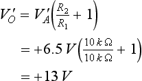
The fully simplified circuit is shown in Figure 9.3(c). Our equivalent circuit reconnected to the amplifier portion of the circuit is shown in Figure 9.3(d). The output voltage can be easily computed by applying our basic gain equation.
This value confirms the correct operation of our adder, which should provide the algebraic sum of its inputs (i.e., +2 V + 12 V − 8 V = +6 V).
9.1.3 Practical Design Techniques
Let us now design a noninverting adder that will satisfy the following design goals:
| 1. Accept four inputs | −10 volts < sum < + 10 volts |
| 2. Minimum input impedance | > 6 kilohms |
| 3. Frequency range | 0 to 1 kilohertz |
Select the Value for R1 and for R3 to R6.
The design of the noninverting adder circuit is very straightforward, since all resistor values are the same with the single exception of the feedback resistor. Selection of the common resistor value is made by considering the following guidelines:
1. High-value resistances magnify the nonideal op amp characteristics and make the circuit more susceptible to external noise.
2. Low-resistor values present more of a load on the driving circuits.
Resistor selection will determine the input impedance presented to the various signal sources as expressed by Equation (9.1).
where R is the common resistor value and N is the number of inputs to the adder circuit. Since the design goal specifies a minimum input of 6 kilohms, let us substitute this value into Equation (9.1) and solve for the value of R.

This represents the smallest value that we can use for the input resistors and still meet our input impedance requirement. Let us choose to use 5.6-kilohm resistors for R1 and for R3 to R6.
Calculate the Feedback Resistor.
The value of the feedback resistor must be selected such that the voltage gain is equal to the number of inputs. In our case we will need a gain of 4. Since we already know the value of R1, we can transpose our basic noninverting amplifier gain equation to determine the value of feedback resistor.
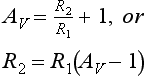
Since voltage gain will always be equal to the number of inputs, this can also be written as
In our case, we can compute the required value of R2 as
If we expect the adder to generate the correct sum, it is essential to keep the resistor ratios correct. Therefore, since 16.8 kilohms is not a standard value, we will need to use a variable resistor for R2 or some combination of fixed resistors (e.g., 15 kΩ in series with 1.8 kΩ).
Select an Op Amp.
There are several nonideal op amp parameters that may affect the proper operation of the noninverting adder. An op amp should be selected that minimizes those characteristics most important for a particular application. The various nonideal parameters to be considered are discussed in Chapter 10. In general, if DC signals are to be added, an op amp with a low offset voltage and low drift will likely be in order. For AC applications, bandwidth and slew rate are two important limitations to be considered.
Based on the modest gain/bandwidth requirements for this particular application, let us use a standard 741 op amp. Other, more precision devices can be substituted to optimize a particular characteristic (e.g., low noise). Many of these alternate devices are pin compatible with the basic 741.
The final schematic diagram of our noninverting adder design is shown in Figure 9.4. The measured performance is contrasted with the original design goals in Table 9.1. It should be noted that the noninverting adder is particularly susceptible to component tolerances and nonideal op amp parameters (e.g., bias current and offset voltage). For reliable operation, components must be carefully selected and good construction techniques used.

9.2 SUBTRACTOR
Another circuit that performs a fundamental arithmetic operation is the subtractor. This circuit generally has two inputs (either AC or DC) and produces an output voltage that is equal to the instantaneous difference between the two input signals. Of course, this is the very definition of a difference amplifier, which is another name for the subtractor circuit.
9.2.1 Operation
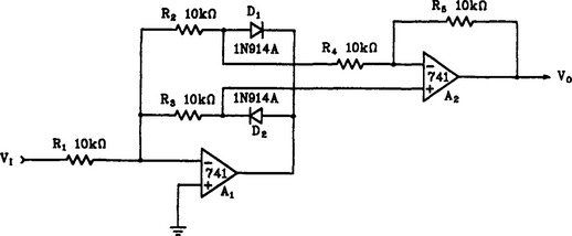
Figure 9.5 shows the schematic diagram of a basic subtractor circuit. A simple way to view the operation of the circuit is to mentally apply the Superposition Theorem (without numbers). If we assume that VA is 0 volts (i.e., grounded), then we can readily see that the circuit functions as a basic inverting amplifier for input VB. The voltage gain for this input will be determined by the ratio of resistors R1 and R2. If we assume that the voltage gain is −1, then the output voltage will be −VB volts as a result of the VB input signal.
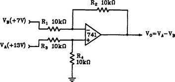
In a similar manner, we can assume that input VB is grounded. In this case, we find that the circuit functions as a basic noninverting amplifier with respect to VA. The overall voltage gain for the VA input will be determined by the ratio of R1 and R2 (sets the op amp gain) and the ratio of R3 and R4, which form a voltage divider on the input. If we assume that the voltage divider reduces VA by half, and we further assume that the op amp provides a voltage gain of 2 for voltages on the (+) input, then we can infer that the output voltage will be +VA volts as a result of the VA signal.
According to the Superposition Theorem, the output should be the net result of the two individual input signals. That is, the output voltage will be +VA − VB. Thus, we can see that the circuit does indeed perform the function of a subtractor circuit.
9.2.2 Numerical Analysis
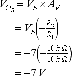
The numerical analysis of the subtractor circuit is straightforward and consists of applying the Superposition Theorem. Let us first assume that the VA input is grounded and compute the effects of the VB input. The output will be equal to VB times the voltage gain of the inverting amplifier circuit, which is
Now let us ground the VB input and compute the output voltage caused by the VA input. First, VA is reduced by the voltage divider action of R3 and R4. The voltage appearing on the (+) input is computed with the basic voltage divider equation.
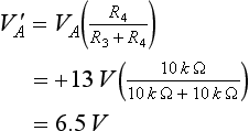
The voltage on the (+) input will now be amplified by the voltage gain of the noninverting op amp configuration, which is
The actual output voltage will be the algebraic sum of the two partial outputs computed:
This, of course, is the result that we would expect from a circuit that is supposed to compute the difference between two input voltages.
The input impedance for the inverting input (VB signal) can be computed with Equation (2.7). For the circuit shown in Figure 9.5, we can compute the inverting input resistance as
The input impedance presented to the noninverting input is essentially the value of R3 and R4 in series. That is,
If resistors R3 and R4 are quite large, then a more accurate value can be obtained by considering that the input resistance of the op amp itself is in parallel with R4. The small signal bandwidth of the circuit can be computed by applying Equation (2.22) to the (+) input. For our present circuit, we can estimate the bandwidth as
The highest practical operating frequency may be substantially lower than this because of slew rate limiting of larger input signals. If we assume that the output will be required to make the full output swing from +VSAT (+13 V) to −VSAT (−13 V), then we can apply Equation (2.11) to determine the highest input frequency that can be applied without slew rate limiting.
9.2.3 Practical Design Techniques
Now let us design a subtractor circuit that will satisfy the following design goals:
| 1. Input voltages | 0 to +5 volts |
| 2. Input frequency | 0 to 10 kilohertz |
| 3. Input impedance | ≥2.5 kilohms |
Compute R1 to R4.
The value of R1 is determined by the minimum input impedance of the circuit. Its value is found by applying Equation (2.7).
Resistors R2 through R4 are set equal to R1 in order to provide the correct subtractor performance. We will use standard values of 2.7 kilohms for these resistors.
Select the Op Amp.
The primary considerations for op amp selection are slew rate and bandwidth. Unless the input signals are very small, the slew rate establishes the upper frequency limit. The required slew rate to meet the design specifications can be found by applying Equation (2.11). The maximum output voltage change will be 10 volts and the frequency may be as high as 10 kilohertz.
This is within the range of the standard 741 op amp. The unity gain frequency required to meet the bandwidth requirements can be estimated with Equation (2.22). In the present case, the minimum unity gain frequency is computed as
which is well below the 1.0-megahertz unity gain frequency of the standard 741. Let us use this device in our design.
There are several other nonideal op amp parameters that could play a significant role in op amp selection. These factors are discussed in Chapter 10.
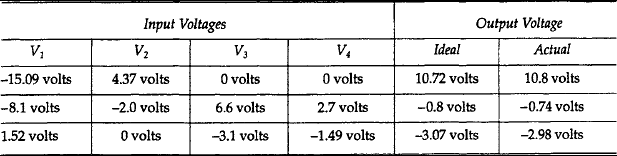
The schematic of our subtractor design is shown in Figure 9.6. Its performance with two in-phase AC inputs is shown in Figure 9.7, where channels 1 and 2 of the oscilloscope are connected to the VA and VB inputs, respectively, and channel 4 shows the output of the op amp, which is the desired function (VO = VA − VB). The response of the circuit to DC signals is listed in Table 9.2.

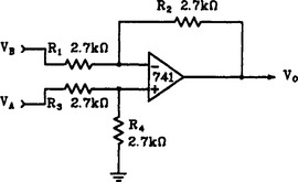
FIGURE 9.6 A subtractor circuit designed for 10-kilohertz operation with 0-volt to 5-volt input signals.
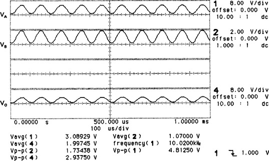
FIGURE 9.7 Oscilloscope display showing the actual performance of the subtractor circuit shown in Figure 9.6. (Test equipment courtesy of Hewlett-Packard Company.)
9.3 AVERAGING AMPLIFIER
The schematic diagram of an inverting averaging amplifier is shown in Figure 9.8. Although this represents a separate mathematical operation, the configuration of the circuit is similar to that of the inverting adder or inverting summing amplifier discussed in Chapter 2.
Since its operation and design are nearly identical to that of the inverting summing amplifier, only a brief analysis will be given here.
To understand the operation of the averaging amplifier, let us apply Ohm’s and Kirchhoff’s Laws along with some basic equation manipulation. Since the inverting input (−) is a virtual ground point, each of the input currents can be found with Ohm’s Law.
Negligible current flows in or out of the (−) input pin, so Kirchhoff’s Current Law will show us that the sum of the input currents must be flowing through R3. That is,

The voltage across R3 will be equal to the output voltage, since one end of R3 is connected to a virtual ground point and the other end is connected directly to the output terminal. Therefore, we can conclude that
Now, for proper operation of the averaging circuit, all of the input resistors must be the same value; let us call this value R. Further, the feedback resistor (R3) is chosen to be equal to R/N where N is the number of inputs to be averaged. Making these substitutions in our previous equations gives us the following:
This final expression for the output voltage should be recognized as the equation for computing arithmetic averages. That is, add the numbers (input voltages) together and divide by the number of inputs. The minus sign simply shows that the signal is inverted in the process of passing through the op amp circuit.
9.4 ABSOLUTE VALUE CIRCUIT
An op amp circuit can be configured to provide the absolute value (| VALUE |) of a given number. You will recall from basic mathematics that an absolute value function produces the magnitude of a number without regard to sign. In the case of an op amp circuit designed to generate the absolute value of its input, we can expect the output voltage to be equal to the input voltage without regard to polarity. So, for example, a +6.2-volt input and a −6.2-volt input both produce the same (typically +6.2-volt) output.
9.4.1 Operation
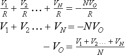
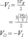
There are several ways to obtain the absolute value of a signal. The schematic diagram in Figure 9.9 shows one possible way. The first stage of this circuit is a dual half-wave rectifier, the same as that analyzed in Chapter 7. Recall that on positive input signals, the output goes in a negative direction and forward-biases D1. This completes the feedback loop through R2. Additionally, the forward voltage drop of D1 is essentially eliminated by the gain of the op amp. That is, the voltage at the junction of R2 and D1 will be the same magnitude (but opposite polarity) as the input voltage.
When a negative input voltage is applied to the dual half-wave rectifier circuit, the output of the op amp goes in a positive direction. This forward-biases D2 and completes the feedback loop through R3. Diode D1 is reverse-biased. In the case of the basic dual half-wave rectifier circuit, the voltage at the junction of R3 and D2 is equal in magnitude (but opposite in polarity) to the input voltage. In the case of the circuit in Figure 9.9, however, this voltage will be somewhat lower because of the loading effect of the current flowing through R2, R4, and R5.
The outputs from the dual half-wave rectifier circuit are applied to the inputs of a difference amplifier circuit. Since the two half-wave signals are initially 180° out of phase, and since only one of them gets inverted by amplifier A2, we can conclude that the two signals appear at the output of A2 with the same polarity. In other words, both polarities of input signal produce the same polarity of output signal. By definition, this is an absolute value function.
9.4.2 Numerical Analysis
Now let us extend our understanding of the absolute value circuit shown in Figure 9.9 to a numerical analysis of its operation. First notice that all resistors are the same value, which greatly simplifies our algebraic manipulation. We will analyze the circuit for both polarities of input voltage.
Figure 9.10 shows an equivalent circuit that is valid whenever V1 is positive. The ground on the lower end of R3 is provided by the virtual ground at the (−) input of A1. It is easy to see that we now have two inverting amplifiers in cascade, so the output voltage will be equal to the input voltage times the voltage gains of the two amplifiers. That is,
Since all resistors are the same value (R), we can further simplify the expression for VO.
FIGURE 9.10 An equivalent circuit for the diagram shown in Figure 9.9 during times when V1 is positive.
In the case of positive input signals, the output voltage is equal to the input voltage.
Now let us consider the effects of negative input voltages. Figure 9.11 shows an equivalent circuit that is valid whenever VI is negative. Kirchhoff’s Current Law, coupled with our understanding of basic op amp operation, allows us to establish the following relationship:
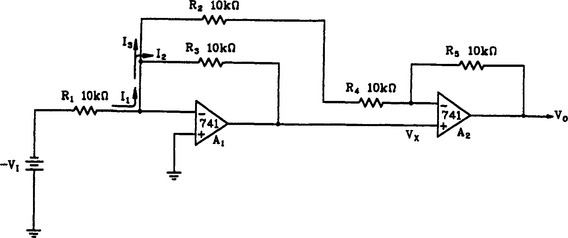
FIGURE 9.11 An equivalent circuit for the diagram shown in Figure 9.9 during times when VI is negative.
Ohm’s Law can be used to substitute resistance and voltage values.
Since all resistor values are equal (R), we can further simplify this latter expression as follows:

We will come back to this equation momentarily. For now, though, let us determine the output voltage in terms of VX. Amplifier A2 is a basic noninverting amplifier with respect to VX, since the left end of R2 connects to ground (virtual ground provided by the inverting input of A1). Therefore, the output voltage can be expressed using our basic gain equation for noninverting amplifiers.
Since the resistors are all equal, we will substitute R for each resistor and solve the equation for VX.

If we now substitute this last expression for VX into our earlier expression, we can determine the output voltage in terms of input voltage. That is,
For negative input voltages, the output is equal in amplitude but opposite in polarity. This, coupled with our previous analysis for positive input voltages, means that the output voltage is positive for either polarity of input voltage and equal in amplitude to the input voltage. Of course, this is the proper behavior for an absolute value circuit where VO = | VI|.
The input impedance, output impedance, frequency response, and so on, are computed in the same manner as are similar circuits previously discussed in detail. These calculations are not repeated here.
9.4.3 Practical Design Techniques
Since all resistor values are the same in the absolute value circuit, the calculations for design are fairly straightforward. Let us design an absolute value circuit that will perform according to the following design goals:
| 1. Input voltage | −10 volts ≤ VI ≤ 10 volts |
| 2. Input impedance | >18 kilohms |
| 3. Frequency range | 0 to 100 kilohertz |
Select the Value for R.
The minimum value for all of the resistors is determined by the required input impedance. The maximum value is limited by the nonideal characteristics of the circuit (refer to Chapter 10), but is generally below 100 kilohms. The minimum value for R can be found by applying Equation (2.7).
Select the Op Amps.
As usual, slew rate and small signal bandwidth are used as the basis for op amp selection. The required unity gain frequency for A2 can be computed with Equation (2.22).

The bandwidth for A1 will be somewhat lower because it has a voltage gain of −1. But in either case, the standard 741 will be more than adequate with regard to bandwidth.
The required slew rate for either amplifier can be computed with Equation (2.11). The voltage and frequency limits are stated in the design goals.
This slew rate exceeds the capability of the standard 741, but falls within the 10-volts-per-microsecond slew rate capability of the MC1741SC. Let us utilize this device in our design. It should be noted that in critical applications several additional nonideal op amp characteristics should be evaluated before a particular op amp is selected. These characteristics are discussed in Chapter 10.
The final schematic diagram for our absolute value circuit is shown in Figure 9.12. Its performance is evident from the oscilloscope displays in Figure 9.13. In Figure 9.13(a) the input is a sinewave. Since both polarities of input translate to a positive output, we have essentially built an ideal full-wave rectifier circuit. Figure 9.13(b) shows the circuit’s response to a very slow (essentially varying DC) triangle wave.
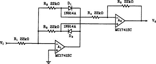
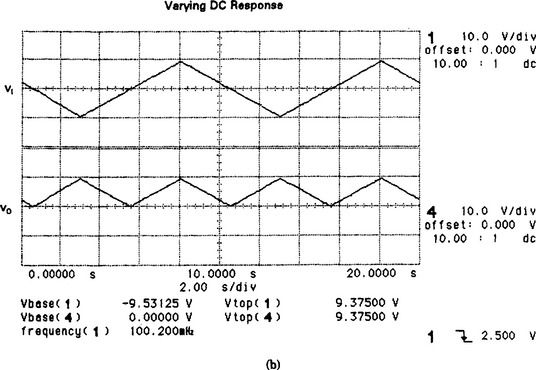
FIGURE 9.13 Oscilloscope displays showing the performance of the absolute value circuit shown in Figure 9.12. (Test equipment courtesy of Hewlett-Packard Company.)
9.5 SIGN CHANGING CIRCUIT
A sign changing circuit is a simple, but important, member of the arithmetic circuits family. Many arithmetic operations require sign or polarity changes. A sign changing circuit, then, is one that can either invert a signal or, alternately, pass it through without inversion. A specific application that could utilize a sign changing circuit is a combination add/subtract circuit. You will recall the basic rule for algebraic subtraction, “… change the sign of the subtrahend and then proceed as in addition.” We could, therefore, route one of the adder inputs through a sign changing circuit that could invert or not invert the signal to subtract or add, respectively.
9.5.1 Operation
The schematic diagram of a sign changing circuit is shown in Figure 9.14. The single-pole double-throw (SPDT) switch is generally an analog switch controlled by another circuit (e.g., a microprocessor system). When the switch is in the upper position, the amplifier is configured as a basic inverting amplifier. The gain (AV = −1) is determined by the ratio of R1 and R2.

When the switch is moved to the lower position, the circuit is configured as a simple voltage follower (AV = 1). Resistor R3 determines the input impedance of the circuit. Its value can be selected such that the input impedance offered by the sign changer is the same in both modes, allowing the circuit to present a constant load on the driving stage. Resistor R1 is open-circuited in the noninverting mode and has no effect on circuit operation.
9.5.2 Numerical Analysis
The numerical analysis for this circuit must be done in two stages (one for each position of the switch). Each of these calculations is literally identical to the calculations presented in Chapter 2 for inverting and noninverting amplifiers, so they are not repeated here.
9.5.3 Practical Design Techniques
Let us now design a simple sign changer circuit that satisfies the following design requirements:
| 1. Input impedance | ≥ 47 kilohms |
| 2. Frequency range | 0−8.5 kilohertz |
Compute R1 and R2.
The value of R1 is established by the input impedance requirement. Its value is computed with Equation (2.7).
Let us choose a standard value of 100 kilohms. Resistor R2 will be the same value as R1, since we want the circuit to have a voltage gain of −1.
Compute R3.
The value of R3 should be equal to the value of R1 so that we can maintain a constant input impedance for both modes. Therefore,
It should be noted that this selection does not minimize the effects of input bias current. The ideal value for R3 is different for the two modes if we want to minimize those effects.
Select the Op Amp.
We will select the op amp on the basis of bandwidth and slew rate. The minimum unity gain frequency is found as
This value should be doubled (i.e., 17 kHz) for critical applications. The minimum required slew rate (based on a full output swing) is calculated with Equation (2.11).
The bandwidth specification can be satisfied by most any op amp. The required slew rate, however, exceeds the 0.5-volts-per-microsecond rating for the standard 741. Let us plan to use an MC1741SC device, which satisfies both bandwidth and slew rate requirements.
The schematic of our sign changing circuit is shown in Figure 9.15. Its performance is evident from the oscilloscope displays shown in Figure 9.16. The waveforms in Figure 9.16(a) show the circuit’s performance in the invert mode. Figure 9.16(b) shows the circuit operated in the noninvert mode.

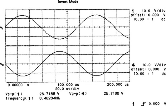
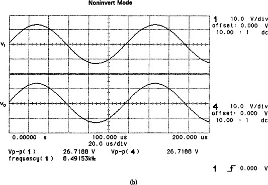
FIGURE 9.16 Oscilloscope displays showing the actual performance of the sign-changing circuit shown in Figure 9.15. (Test equipment courtesy of Hewlett-Packard Company.)
9.6 TROUBLESHOOTING TIPS FOR ARITHMETIC CIRCUITS
Most of the arithmetic circuits presented in this chapter are electrically similar to other amplifier circuits previously studied; it is the component values and intended application that cause them to be classified as arithmetic. With this in mind, all of the troubleshooting tips and procedures previously discussed for similar circuits are applicable to the companion arithmetic circuits and will not be repeated here.
Proper operation of the arithmetic circuits presented in this chapter requires accurate component values. It is common to use precision resistors to obtain the desired performance. If a component changes value, its effects may be more noticeable in the arithmetic circuits than in similar, nonarithmetic circuits previously discussed. The very nature of the arithmetic circuit generally implies a higher level of required accuracy than that for a simple amplifier. Thus, the probability of problems being caused by component variations is greater with arithmetic circuits.
To diagnose a problem caused by a component variation, it is helpful to apply your theoretical understanding of the circuit to minimize the number of suspect components. By applying various combinations of signals and monitoring the output signal, you can usually identify a particular input that has an incorrect response. If, on the other hand, all of the inputs seem to be in error (e.g., shifted slightly), then the problem is most likely a component that is common to all inputs (e.g., the feedback resistor or op amp).
If your job requires you to do frequent maintenance on arithmetic circuits, it is probably worth your while to construct a test jig to aid in diagnosing faulty circuits. The test jig could consist of a number of switch-selectable voltages applied to several output jacks, and the voltages should be accurate enough to effectively test the particular class of circuits being evaluated. The jig, coupled with a table showing the performance of a known good circuit, can be used to very quickly isolate troubles in arithmetic circuits. Of course, this entire test fixture could easily be interfaced to a computer for automatic testing and comparison.
If the circuit seems to work properly in the laboratory, but consistently goes out of tolerance when placed in service, you might suspect a thermal problem. Nearly all of the components in all of the circuits are affected by temperature changes. Short of providing a constant temperature environment, your only options for improving performance under changing temperature conditions are these:
You can artificially simulate temperature changes to a single component by spraying a freezing mist on it. Sprays of this type are available at any electronics supply store. Although every component you spray may cause a shift in operation, an abrupt or dramatic or erratic response from a particular one may indicate a failing part.
There are numerous choices for all of the components in the circuits presented in this chapter. Improved immunity to temperature variations can often be obtained simply by substituting components with more stringent tolerances. Resistors with a 5-percent rating can be replaced, for example, with 1-percent resistors. Similarly, a general-purpose op amp can be replaced with a pin-compatible op amp having lower bias currents, noise, or temperature coefficients.
Finally, if items 1 and 2 in the list above do not resolve a particular thermal problem, then redesign may be in order. Frequently, there is a trade-off between circuit simplicity and circuit stability. Achieving rock-solid stability often requires a step increase in circuit complexity.
REVIEW QUESTIONS
1. Refer to Figure 9.2. What is the effect on circuit operation if resistors R3 to R5 are all increased to 20 kilohms?
2. Refer to Figure 9.2. Show how the circuit can be analyzed by applying the Superposition Theorem to the input circuit.
3. Refer to Figure 9.5. What is the effect on circuit operation if resistor R3 develops an open?
4. Refer to Figure 9.5. What is the effect on circuit operation if resistor R2 develops an open?
5. Refer to Figure 9.9. What is the effect on circuit operation if resistor R3 is doubled in value?
6. Refer to Figure 9.9. Describe the effect on circuit operation if resistor R4 becomes open.
7. Will the circuit shown in Figure 9.9 still operate correctly if resistors R4 and R5 are both doubled in value? Explain your answer.