
CHAPTER NINE
RF Power Amplifiers
9.1 TRANSISTOR CONFIGURATIONS
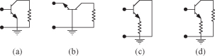
In Chapter 8, class A amplifiers were treated. Some discussion was given to its application as a power amplifier. While class A amplifiers are used in power applications where linearity is of primary concern, they do so at the cost of efficiency. This chapter describes power amplifiers that provide higher efficiency than the class A amplifier. Before describing these in detail, it should be recalled that a single-transistor amplifier can be installed in one of four different ways: common emitter, common base, common collector (or emitter follower), and common emitter with emitter degeneracy. Although there are always exceptions, the common emitter circuit is used in amplifiers where high-voltage gain is required. The common base amplifier is used when low input impedance and high output impedance is desired. This is accompanied with a current gain ≈ 1. The emitter follower is used when high input impedance and low output impedance is desired. This is accompanied with a voltage gain ≈ 1. The common emitter with emitter degeneracy configuration is used when improved repeatability is needed with respect to differences in the transistor short-circuit current gain (β). The emitter resistance provides negative feedback and thus causes some loss in voltage gain. These configurations (minus bias circuits) are illustrated in Fig. 9.1. These properties are described in detail in most electronics texts.
FIGURE 9.1 Connections for (a) common emitter, (b) common base, (c) common collector or emitter follower, and (d) common emitter with emitter degeneracy.
The transistor itself can be in one of four different states: saturation, forward active, cutoff, and reverse active. It is in the forward active region, when for the bipolar transistor, the base–emitter junction is forward biased and the base–collector junction is reverse biased. These states are illustrated in Fig. 9.2 for an npn transistor. An actual bipolar transistor requires a base–emitter voltage greater than 0.6 to 0.8 V for it to go into the active state. For MOSFETs the gate–source voltage must exceed the threshold voltage, υt.
FIGURE 9.2 Four bias regions for npn bipolar transistor.

The voltage swing of a class A amplifier will remain in the forward active region throughout its entire cycle. If the output signal current is
(9.1)
![]()
and the dc bias current is Idc, then the total instantaneous current is
(9.2)
![]()
The quiescent current, IQ, is the current around which the alternating current flows. For the class A amplifier, ![]() , so that the entire waveform of the ac signal is amplified without distortion. The conduction angle is 360°. For the power amplifiers under consideration in this chapter, the transistor(s) will be operating during part of their cycle in either cutoff or saturation or both.
, so that the entire waveform of the ac signal is amplified without distortion. The conduction angle is 360°. For the power amplifiers under consideration in this chapter, the transistor(s) will be operating during part of their cycle in either cutoff or saturation or both.
9.2 CLASS B AMPLIFIER
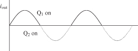
The class B amplifier is biased so that the transistor is on only during half of the cycle of the incoming signal. The other half of the cycle is amplified by another transistor so that at the output the full wave is reconstituted. This is illustrated in Fig. 9.3. While each transistor is clearly operating in a nonlinear mode, the total input wave is directly replicated at the output. The class B amplifier is therefore classed as a linear amplifier. In this case, the quiescent current, IQ = 0. Since only one of the transistors is cut off when the total voltage is less than 0, only the positive half of the wave is amplified. The conduction angle is 180°. The term class AB amplifier is sometimes used to describe the case when the direct quiescent current is much smaller than the signal amplitude, ![]() , but still greater than 0. In this case,
, but still greater than 0. In this case,
![]()
FIGURE 9.3 Reconstituted waveform of class B amplifier.
9.2.1 Complementary (npn/pnp) Class B Amplifier
The illustration in Fig. 9.4a shows a complementary type of class B amplifier. In this case transistor Q1 is biased so that it is in the active mode when the input voltage is greater than the transistor turn-on voltage, υin > 0.7, and cut off when the input signal υin < 0.7. The other half of the signal is amplified by transistor Q2 when υin < −0.7. When no input signal is present, no power is drawn from the bias supply through the collectors of Q1 or Q2 so the class B operation is attractive when low standby power consumption is an important consideration. There is a small region of the input signal for which neither Q1 nor Q2 are on. The resulting output will therefore suffer some distortion.
FIGURE 9.4 Complementary class B amplifier: (a) the basic amplifier, (b) compensation to reduce crossover distortion, and (c) amplifier with VBE multiplier to reduce crossover distortion.
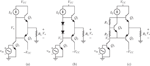
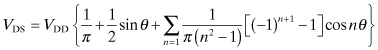
The npn transistor Q1 in the class B circuit in Fig. 9.4a has its collector connected to the positive power supply, VCC, and its emitter connected to the load, RL. The collector of the pnp output transistor, Q2, has its collector connected to the negative supply voltage VEE, which is often equal to −VCC, and its emitter also connected to the load, RL. The bases of Q1 and Q2 are connected together and are driven by the collector of the input transistor Q3. The input transistor, Q3, has a bias current source, Ibias, feeding its collector, which also provides base current for Q1. The input voltage, υin to the input transistor Q3 is what drives the output stage. It is tempting when doing hand or SPICE calculations to start with υin. However, because a small change in the base voltage of Q3 makes a large change in the collector voltage of Q3, it is easier to start the analysis at the base of Q2. This base voltage is Vx in Fig. 9.4.
When Vx = 0, both output transistors Q1 and Q2 are turned off because the voltage is less than the 0.7 V necessary to turn the transistors on. If Vx > 0.7, then Q1 (npn) is on and Q2 (pnp) is off. Current is then drawn from the power supply, VCC, through Q1 to produce the positive half-wave of the signal in the load. If Vx < 0.7, then Q1 (npn) is off and Q2 (pnp) is on. The voltage Vx is made negative by turning Q3 on, thus bringing the collector voltage of Q3 closer to VEE, which is less than zero. An extreme positive or negative input voltage puts the turned-on output transistor (either Q1 or Q2) into saturation. The maximum positive output voltage is
(9.3)
![]()
and the maximum negative output voltage is
(9.4)
![]()
Typically, the value for VCE(sat) ≈ 0.2 V for a bipolar transistor. More design details are available from a variety of sources, such as [1].
9.2.2 Elimination of the Dead Band
The 1.2- to 1.4-V range in the base voltages of Q1 and Q2 can be substantially compensated by addition of two diodes in series between the bases of Q1 and Q2 (Fig. 9.4b). These diodes are named, respectively, D4 and D5. For purposes of calculation, let Vx stand for the voltage at the collector of the driver transistor Q3, which is the same as the base voltage for the pnp output transistor Q2. To get to the base of Q1 from Vx now requires going through the two series-connected diodes “backward” from cathode to anode. If Vx > 0 but not so high as to turn off the diodes D4 and D5, then Q1 is on as inferred from Fig. 9.4a. The voltage across the load is
(9.5)
![]()
to make Vx < 0. The input voltage to the driver Q3 must be a positive voltage. The npn output transistor Q1 is turned off, and the excess bias current from Ibias flows through the diodes D4 and D5 and then through the now turned-on Q3. In this case the output voltage is not now affected directly by the diode:
(9.6)
![]()
Under this condition, the value of Vx is actually a negative number. In the middle where Vx = 0, the output voltage across RL is
(9.7)
![]()
and
(9.8)
![]()
In either case, the output voltage is the voltage drop across one pn junction. If the forward diode voltage drops are equal to the base–emitter drops of the transistors, there is no discontinuity in Vo in going from negative to positive input voltages.
In actual production circuits, tight specifications are needed on diodes D4 and D5 since they are in the base circuit of the output transistors and consequently carry much less current than the output power devices. The discrepancy between the high-power and low-power devices can be alleviated by using the VBE multiplier shown in Fig. 9.4c. In this circuit the base–emitter voltage of Q4 sets the current through R2:
(9.9)
![]()
Assuming the base current of Q4 is negligible, the voltage drop between the bases of the output transistors Q1 and Q2 is
(9.10)
![]()
When the voltage at the base of Q2 is positive, the load voltage is
(9.11)
![]()
and when Vx < 0,
(9.12)
![]()
In the middle when Vx = 0, the ![]() and
and ![]() can be forced to be equal by adjustment of the resistors R1 and R2:
can be forced to be equal by adjustment of the resistors R1 and R2:
(9.13)
![]()
In addition to reducing or eliminating the dead-band zone, the compensation circuits in Figs. 9.4b and 9.4c also provide for temperature stability, since a change in the temperature changes the transistor VBE value. The compensation circuit and the power transistors vary in the same way with temperature since they are physically close together.
Another aspect that deserves attention is the actual value of the current source, Ibias. Since this supplies the base current for the npn output transistor Q1, Ibias must be large enough to not “starve” Q1 when it is drawing the maximum current through its collector. This means that IQ ≥ IC1/β1.
9.2.3 Composite pnp Transistor
One of the primary problems in using this type of class B amplifier is the requirement for obtaining two equivalent complementary transistors. Fundamentally, the problem arises because of the greater mobility of electrons by over a 3 : 1 factor over that of holes in silicon. The symmetry of the gain in this circuit depends on the two output transistors having the same small-signal short-circuit base-to-collector current gain, β = ic/ib. When it is not possible to obtain a high-β pnp transistor, it is sometimes possible to use a composite transistor connection. A high-power npn transistor, Q1, is connected to a low-power low-β pnp transistor, Q2, as shown in Fig. 9.5. Normally, the base–emitter junctions of the composite and single pnp transistor are forward biased so that the Shockley diode equation may be used to describe the bias currents. For Q2 in the composite circuit,
(9.14)
![]()
FIGURE 9.5 Composite connection for pnp transistor.
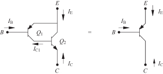
The collector current for Q1 in the composite circuit is the same as the collector current for the single pnp transistor:
(9.15)
![]()
The composite circuit has the polarity of a pnp transistor with potentially the gain of an npn transistor.
9.2.4 Small-Signal Analysis
The three fundamental parameters that characterize an amplifier are its voltage gain, Av, input resistance, Ri, and output resistance, Ro. In the circuit shown in Fig. 9.4a, neither Q1 nor Q2 are on simultaneously. If Q1 is on, Q2 is an open circuit and need not be considered as part of the ac analysis. A small-signal hybrid π model (Fig. 9.6) for a bipolar transistor consists of a base resistance, rb, base–emitter resistance, rπ, collector–emitter resistance, ro, transconductance, gm, and short-circuit current gain β = gmrπ. There are in addition high-frequency effects caused by reactive parasitic elements within the device. Since the voltage gain of an emitter follower is ≈1, the voltage gain of the Q3 and Q1 combination is
(9.16)
![]()
FIGURE 9.6 Small signal hybrid π model of bipolar transistor.
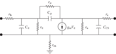
The effective load resistance RL(eff) seen by the first transistor, Q3, is the same as the input resistance of the emitter follower circuit Q1. Circuit analysis of the low-frequency transistor hybrid model shown in Appendix F gives
(9.18)
![]()
The voltage gain is then found by substitution:
(9.19)
![]()
(9.20)
![]()
The low-frequency input resistance to the actual class B amplifier is given by RL(eff) in Eq. (9.17), and the output resistance is
(9.21)
![]()
Thus, the input resistance is high and the output resistance is low for a class B amplifier, which enables it to drive a low-impedance load with high efficiency.
9.2.5 All-npn Class B Amplifier
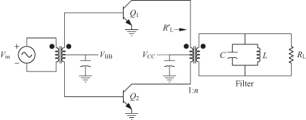
The complementary class B amplifier shown in Fig. 9.4 needs to have symmetrical npn and pnp devices. In addition this circuit also requires complementary power supplies. These two problems can be alleviated by using the totem pole or all npn transistor class B amplifier. This circuit requires only one power supply and has identical npn transistors that amplify both the positive and negative halves of the signal. However, it requires that the two transistors operate with an input phase differential of 180°. This circuit is illustrated in Fig. 9.7. Clearly, the cost of the all-npn transistor amplifier is the added requirement of two center-tapped transformers. These are necessary to obtain 180° phase difference between Q1 and Q2. The center-tapped transformer also provides dc isolation for the load. When the input voltage is positive, Q1 is on and Q2 is off. When the input voltage is negative, the input transformer induces a positive voltage at the “un-dotted” secondary winding, which turns Q2 on. The output of Q2 will induce on the output transformer a positive voltage on the un-dotted terminal and a negative voltage on the “dotted” terminal. The negative input voltage swing is thus replicated as a negative voltage swing at the output. The transformer turns ratio can be used for impedance matching. The output filter is used to filter out any harmonics caused by crossover or other sources of distortion. The filter is not necessary to achieve class B operation, but it can be helpful.
FIGURE 9.7 All npn class B amplifier.
9.2.6 Class B Amplifier Efficiency
The maximum efficiency of a class B amplifier is found by finding the ratio of the output power delivered to the load to the required dc power from the bias voltage supply. In determining efficiency in this way, power losses caused by nonzero base currents and crossover distortion compensation circuits used in Figs. 9.4b and 9.4c are neglected. Furthermore, the power efficiency (or collector efficiency) rather than the power-added efficiency is calculated so as to form a basis for comparison for alternative circuits. It is sufficient to do the calculation during the part of the cycle when Q1 is on and Q2 is off. The load resistance in Fig. 9.7 is transformed through to the primary side of the output transformer, loading the transistors with a value of ![]() . Since the transformer is assumed lossless, referring the load resistance to the primary side,
. Since the transformer is assumed lossless, referring the load resistance to the primary side, ![]() will not change the efficiency.
will not change the efficiency.
The peak magnitude of the collector current that flows into ![]() is
is ![]() . The alternating current is
. The alternating current is
(9.22)
![]()
and the peak voltage is
(9.23)
![]()
Since the collector–base voltage must remain positive to avoid the danger of burning out the transistor, ![]() . The maximum allowable output power delivered to the load is
. The maximum allowable output power delivered to the load is
(9.24)
![]()
A determination of the direct current supplied by the bias supply is needed. The magnitude of the current delivered by the bias supply to the load by Q1 is
(9.25)
![]()
and for Q2
(9.26)
![]()
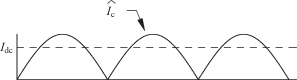
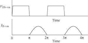
The total current is then ![]() , which is shown in Fig. 9.8. The direct current from the bias sources is found by finding the average current:
, which is shown in Fig. 9.8. The direct current from the bias sources is found by finding the average current:
(9.27)
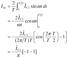
(9.28)
![]()
FIGURE 9.8 Waveform for finding average dc from power supply.
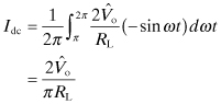
The power drawn from both of the power supplies by both of the output transistors is
(9.29)
![]()
Thus, the output power is proportional to ![]() and is the average power drawn from the power supply. The power delivered to the load is
and is the average power drawn from the power supply. The power delivered to the load is
(9.30)

The efficiency is the ratio of these latter two values:
(9.31)
(9.32)
![]()
The maximum output power occurs when the output voltage is VCC − VCE(sat):
(9.33)

(9.34)
![]()
This efficiency for the class B amplifier should be compared with the maximum efficiency of a class A amplifier where ηmax = 25% when the bias to the collector is supplied through a resistor and ηmax = 50% when the bias to the collector is supplied through an RF choke.
9.3 CLASS C AMPLIFIER
The class C amplifier is useful for providing a high-power continuous wave (CW) output. When it is used in amplitude modulation schemes, the output variation is done by varying the bias supply [2]. There are several characteristics that distinguish the class C amplifier from the class A or B amplifier. First of all, it is biased so that the transistor conduction angle is <180°. Consequently, the class C amplifier is clearly nonlinear in that it does not directly replicate a broadband input signal like the class A and B amplifiers do (at least in principle). The class A amplifier requires one transistor, the class B amplifier requires two transistors, and the class C amplifier uses one transistor. Topologically, it looks similar to the class A except for the dc bias level at the transistor input. It was noted in the class B amplifier, an output filter was used optionally to help clean up the output signal. In the class C amplifier, such a tuned output is necessary in order to recover the sine wave. Finally, class C operation is capable of higher efficiency than either of the previous two cases, so when dealing with the appropriate signal types, they become very attractive as power amplifiers.
The class C amplifier in Fig. 9.9 shows the output circuit for an n-channel enhancement mode MOSFET. A power bipolar transistor might also be used here. The choice between the two lies in the specific design goals for the amplifier. Actually, the analysis that follows for the class C amplifier is based on triode vacuum tubes [3], which were later incorporated by [2]. The Q of the tuned circuit will determine the bandwidth of the amplifier. The large inductance RF coil in the drain voltage supply ensures that only dc current flows there. During that part of the input cycle when the transistor is on, the bias supply current flows through the transistor and the output voltage is approximately 90% of VDD. When the transistor is off, the supply current flows into the blocking capacitor. The current waveform at the drain can be modeled as the waveform shown in Fig. 9.10:
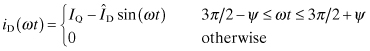
FIGURE 9.9 Simple class C amplifier where VGG determines conduction angle.
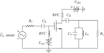
FIGURE 9.10 Drain current waveform for class C operation.
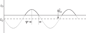
Other approximations have been made for this current waveform based on different device characteristics, but Eq. (9.35) will provide a reasonable analytical solution.
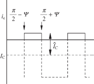
For class C operation, the magnitude of the quiescent current is ![]() . The point where the total current = 0 is
. The point where the total current = 0 is
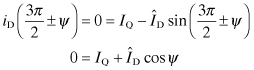
This determines the value of the quiescent current in terms of the conduction angle 2ψ:
The direct current from the power supply is the average of the total drain current iD(θ) where θ = ωt:
(9.38)
Evaluation of the integral makes use of the trigonometric identity, cos(α ± β) = cos α cos β ![]() sin α sin β. From Eq. (9.36) the direct current is
sin α sin β. From Eq. (9.36) the direct current is
(9.39)
![]()
This gives the average of the actual conducting current of the clipped sine wave in Fig. 9.10. The quiescent current, IQ, is the negative bias current around which the alternating current flows if it could. This gives the direct current from the power supply in terms of ![]() and the conduction angle ψ, so that power supplied by the source is
and the conduction angle ψ, so that power supplied by the source is
(9.40)
![]()
The ac component of the current flows through the blocking capacitor and into the load. Harmonic current components are shorted to ground by the tuned circuit. The magnitude of the output voltage at the fundamental frequency is found using the Fourier method. The minus sign is used because the drain current convention draws current up from the load:
(9.41)
(9.42)
(9.43)

The quiescent current term, IQ, is replaced using Eq. (9.37) again, and the trigonometric identity for sin α cos β is used:
(9.44)
![]()
(9.45)
![]()
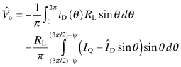
The ac output power delivered to the load is
(9.46)
![]()
The efficiency (neglecting the input power) is simply the ratio of the output ac power to the input dc power. The maximum output power occurs when ![]() . The maximum efficiency is then
. The maximum efficiency is then
(9.47)
![]()
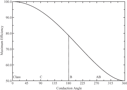
A plot of this expression (Fig. 9.11) clearly illustrates the efficiency in terms of the conduction angle for class A, B, and C amplifiers. The increased efficiency of the class C amplifier is a result of the drain current flowing for less than a half cycle. When the drain current is maximum, the drain voltage is minimum, so the power dissipation is inherently lower than class B or class A operation.
FIGURE 9.11 Power efficiency for class A, B, and C amplifiers.
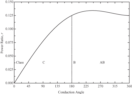
Another important parameter for the power amplifier is the ratio of the maximum average output power where ![]() , to the peak instantaneous output power:
, to the peak instantaneous output power:
The maximum average output power occurs when ![]() and is given by
and is given by
(9.50)
![]()
(9.51)
![]()
The maximum voltage at the drain is the peak output voltage plus the dc bias voltage:
(9.52)
![]()
The maximum current based on Eq. (9.37) is
(9.53)
![]()
The ratio of the maximum average power to the peak power from Eq. (9.49) is
A plot of this ratio as a function of conduction angle in Fig. 9.12 shows that maximum efficiency of the class C amplifier occurs when there is no output power. Figures 9.11 and 9.12 show the trade-offs in choosing the appropriate conduction angle for class C operation.
FIGURE 9.12 Maximum output power to peak power ratio.
9.4 CLASS C INPUT BIAS VOLTAGE
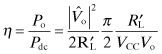
Device SPICE models for RF power transistors are relatively rare. Manufacturers often do supply optimum generator and load impedances that have been found to provide the rated output power for the designated frequency. The circuit shown in Fig. 9.9 is a generic example of a class C amplifier in which the manufacturer has determined empirically the optimum generator and load impedances. The Q of the output tuned circuit is
(9.55)
![]()
The Q then determines the inductance and capacitance of the output shunt resonant circuit:
(9.56)
![]()
(9.57)
![]()
Furthermore, if the desired output power is PQ(max), the drain voltage source, VDD, and the maximum drain current is iD(max), then the average to peak power ratio, r, is found from Eqs. (9.49) and (9.54). Iterative solution of Eq. (9.54) gives the value for the conduction angle, ψ. This will then allow for estimation of the maximum efficiency from Eq. (9.48). Alternatively, for a given desired efficiency, the conduction angle, ψ, can be obtained by iterative solution of Eq. (9.48). Numerically, it is useful to take the natural logarithm of Eq. (9.48) before searching iteratively for a solution:
(9.58)
![]()
The efficiency expression can be modified to account for the nonzero drain–source voltage:
(9.59)
![]()
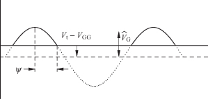
To achieve the desired conduction angle, the gate–source voltage must be biased so that the transistor will be in conduction for the desired portion of the input signal. Drain current flows when the transistor is above cutoff, VGS > Vt. First, it is necessary to determine the required generator voltage amplitude, ![]() , that will produce the desired maximum output current. This is illustrated in Fig. 9.13 where the input ac signal is superimposed on the gate bias voltage. The input voltage commences to rise above the turn on voltage of the transistor at
, that will produce the desired maximum output current. This is illustrated in Fig. 9.13 where the input ac signal is superimposed on the gate bias voltage. The input voltage commences to rise above the turn on voltage of the transistor at
(9.60)
![]()
FIGURE 9.13 Conduction angle dependence on VBB.
In this way the gate bias voltage is determined.
9.5 CLASS D POWER AMPLIFIER
Inspection of the efficiency and output power of a class C amplifier reveals that 100% efficiency only occurs when the input power is zero. A modification of class B operation shown in [4] indicates that a judicious choice of bias voltages and circuit impedances provide a clipped voltage waveform at each output of the transistors while retaining the half sine wave output current. In the limit the clipped voltage waveform becomes a square wave. This is no longer linear and, thus, is distinguished from the class B amplifier.
The class D amplifier shown in Fig. 9.14 superficially looks like a class B amplifier except for the input side bias. In class D operation, the transistors act as near ideal switches that are on half of the time and off half of the time. The transistors may be pulse width modulated to produce an output that does not have a 50% duty cycle. However, in this discussion the input is excited by a square wave. If the transistor switching time is near zero, then drain current flows while the drain–source voltage VDS = 0 and VDS is nonzero when ID = 0. As a result 100% efficiency is theoretically possible. In practice, the switching speed of a transistor is not sufficiently fast at high frequencies to produce square waves using this design.
FIGURE 9.14 Class D power amplifier.
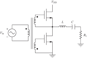
For the circuit shown in Fig. 9.14, the voltage is either at VDD or 0, depending on the phase of the input signal. However, only current at the resonant frequency of the LC resonator can pass on to the load. Since one transistor is on while the other is off, the transistors must either be complementary devices or make use of a center-tapped transformer as shown. This ensures the required 180° phase difference between the inputs of the two transistors. A more practical class D circuit is shown in Fig. 9.15. Both of these circuits are described as voltage mode circuits since the voltage at the input of the filter is approximately a square wave. The waveform of the voltage mode circuit is shown in Fig. 9.16.
FIGURE 9.15 Practical voltage mode class D amplifier.
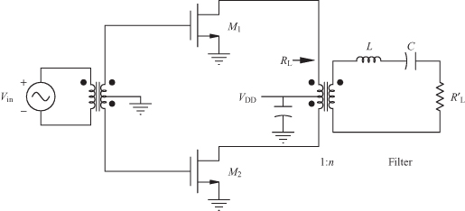
FIGURE 9.16 Voltage and current waveforms for voltage mode (vm) amplifier.
9.5.1 Class D Amplifier Efficiency
The analysis begins by finding the ac power delivered to the load. The Fourier series expansion of the square wave voltage at the input to the LC filter is
where θ = ωt. The current going through the resonant LC circuit is
(9.62)
![]()
Consequently, the RF power delivered to the load is
(9.63)
![]()
The rectified voltage mode current wave shown in Fig. 9.16 is given as
A Fourier expansing of Eq. (9.65) results in
The dc component from Eq. (9.66) is
The amplitude, ![]() , is proportional to the amplitude of the rectified current sine wave, which in turn is determined by the fundamental voltage amplitude, 2VDD /π. From Eq. (9.67)
, is proportional to the amplitude of the rectified current sine wave, which in turn is determined by the fundamental voltage amplitude, 2VDD /π. From Eq. (9.67)
(9.68)
![]()
The dc input power is

The ratio of the RF power in the load from Eq. (9.64) and the dc power from Eq. (9.69) gives an efficiency of 100%.
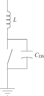
The efficiency of the class D amplifier falls short of the promised 100% because of the presence of parasitic lead inductance and especially the shunt capacitance, CDS. The switching transistors can be modeled as an ideal switch plus these parasitic reactances (Fig. 9.17) [5]. The energy stored in the inductor, Li2/2 and in the capacitor, Cυ2/2, is dissipated during each cycle. The current is not completely zero when the voltage starts to turn on, and the voltage is not completely zero when the current starts to turns on. This overlap gets worse as the operating frequency increases.
FIGURE 9.17 Switching transistor model.
9.5.2 Current Mode Class D Amplifier
Voltage mode operation occurs when the voltage is a square wave and the current a rectified sine wave. Reversing this as suggested by Fig. 9.18 so that the current is a square wave and the voltage a sine wave can increase the operating frequency range significantly. This circuit design was described in [5] and later in a thesis [6]. A circuit schematic for the current mode class D amplifier is shown in Fig. 9.19. The basic idea is to use the parasitic inductance or capacitance (Fig. 9.17) as part of the resonant circuit. The voltage mode circuit can absorb the inductance while the current mode circuit can absorb the capacitance. Since the capacitance is a far larger problem than the inductance, the current mode design is in practice capable of a much higher frequency range.
FIGURE 9.18 Current mode waveforms.
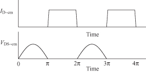
FIGURE 9.19 Current mode class D amplifier.
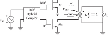
Current mode class D waveforms are shown in Fig. 9.18 and the circuit is shown in Fig. 9.19. The two transistors must be either a complementary pair or they must be excited out of phase with one another. The drain bias for the transistors goes through a choke that permits only a dc current to flow into the transformer center tap. This steady current is switched between the top transistor and the bottom transistor, thereby producing a current square wave. The LC filter will only allow the fundamental ac voltage to appear across the load. All higher voltage harmonic components are shorted to ground by the capacitor, C. Furthermore, C and the CDS from the transistors appear in shunt with one another so that CDS can be made to be part of the resonant circuit.
The square current waveform and the rectified sine voltage waveform can be expanded in a Fourier series much like the voltage mode waveforms were. The choice of origin will change the sign of the harmonic components from that obtained for the voltage mode:
(9.70)
(9.71)
![]()
These two equations are complementary to Eqs. (9.66) and (9.61), respectively. The efficiency can be calculated when the current waveform is less than a perfect square wave. If only the fundamental and one harmonic is considered, the first three terms of these two expressions give
(9.72)
![]()
(9.73)
![]()
Rather than consider the last two equations as a truncated series, they are considered to be the total voltage and current with the restriction that neither one is ever less than zero. This is the technique used in [5]. From the voltage waveform pictured in Fig. 9.18, at θ = 3π/2:
(9.74)
![]()
and for the current at θ = π/2
(9.76)
![]()
The first-order derivatives of the waveforms are zero at VDS(π/2), ID(π/2), and ID(3π/2). However, this yields no new information about the voltage and current amplitudes. The second-order derivative gives the rate of change of the slope. In the flat portion of the waves, the second-order derivative is zero. In particular, the voltage wave is flat at θ = 3π/2:
(9.78)
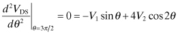
(9.79)
![]()
This along with Eq. (9.75) yields
(9.80)
![]()
(9.81)
![]()
For the current wave, there are two flat spots. Evaluating the second-order derivative at either of these places gives the same result:
(9.82)
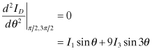
or
(9.83)
![]()
This with Eq. (9.77) yields
(9.84)
![]()
(9.85)
![]()
The above values for the voltage and current components using one harmonic can be used to determine the efficiency. When the VDS from transistor M1 in Fig. 9.19 is high, the fundamental voltage across RL is high. When the VDS from M2 is high the fundamental voltage across RL is low. The ac voltage swing around the input to the center-tapped transformer is 2V1 centered at VDD. For the purposes of calculating efficiency, the transformer is considered lossless. The load resistance transformed to the primary side is ![]() . The total dc current from the power supply to the two transistors is
. The total dc current from the power supply to the two transistors is
(9.86)
![]()
and the dc power is
(9.87)

Since
(9.88)
![]()
then
(9.89)
![]()
The fundamental ac power delivered to the load, ![]() is
is
(9.90)
![]()
(9.91)
![]()
Thus, the drain efficiency is
(9.92)
![]()
This calculation was done using only one harmonic above the fundamental to approximate the current square wave. As the number of harmonics are increased, the more square the current waveform becomes and the closer to 100% efficiency is achieved. Indeed, an analytical expression using two harmonics above the fundamental has been provided in [5]. The major contribution of this study is to show how current mode class D amplifiers can incorporate CDS so that high-efficiency, high-power (in the tens of watts) operation can be practically achieved in the low-gigahertz frequency range [6].
9.6 CLASS E POWER AMPLIFIER
The class E amplifier, like the class D, assumes the transistor acts as an ideal switch rather than a current source. Both the class D and the class E nonlinear amplifiers are capable of achieving 100% efficiency. The major weakness of the class D amplifier is that the frequency of operation is limited by the rise and fall times of the transistor output pulse. The nonzero switching time is a result of parasitic capacitances in the circuit and transistor. Even the current mode class D amplifier will eventually have this difficulty at high frequencies. The class E design turns this liability into a feature, so that high-efficiency operation can be achieved at higher frequencies than that available in the class D circuit.
The class E amplifier concept was first introduced by Ewing [7] in 1964 and later independently rediscovered by Sokal and Sokal [8] in 1975. In 1977 and 1978, Raab derived design equations for the class E amplifier [9, 10]. This work was later expanded to include a relationship between maximum output power and maximum efficiency. The derivation in [9] was done for an arbitrary duty cycle, but it is simpler to assume the duty cycle is 50% as done in [11] and [12] for the simple reason that high-frequency switching is difficult and counterproductive at a duty cycle other than 50%.
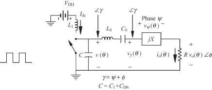
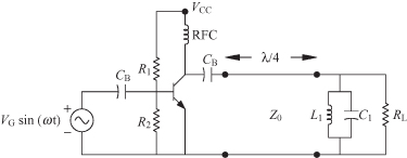
The material in this section on class E amplifiers is largely the result of work done by Cantrell as described in [11] and [12]. The basic feature of the class E amplifier (Fig. 9.20) is to produce a voltage wave across the capacitance shunting the transistor that has zero amplitude and zero slope when the transistor is turned on. This relieves the switching speed requirement of the class D amplifier and yet maintains the possibility of 100% efficiency. The circuit in Fig. 9.20 consists of a transistor that is switched between on and off by the input gate voltage, a choke inductor, L1, to maintain dc current flow, a high Q series resonant circuit, an additional excess reactance, jX, and an external drain to source capacitance, C1. An idealized equivalent circuit is shown in Fig. 9.21. For analysis purposes, the transistor has been replaced by an ideal switch.
FIGURE 9.20 Class E amplifier with switching transistor.

FIGURE 9.21 Ideal class E amplifier with ideal switch used for analysis.
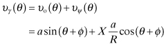
The analysis starts with a pure sine wave at the output and proceeds back toward the input. The output voltage with amplitude a and unspecified phase ϕ is
and the output current is
(9.94)
![]()
The voltage, υγ(θ), is also sinusoidal but with a phase offset γ:
(9.95)
These two terms may be added together by defining b and ψ as
(9.96)
![]()
(9.97)
![]()
then
(9.98)
![]()
(9.99)
![]()
where
(9.100)
![]()
and
(9.101)
![]()
When the switch is turned off, the voltage across the switch results from charging the capacitance C with ic(θ). This voltage is not sinusoidal:
(9.102)
![]()
(9.103)
![]()
In this expression, the susceptance is B = ωC.
At the fundamental frequency the tuned circuit is resonant, so at this frequency υ(θ) = υγ (θ), and the fundamental amplitude of the switch voltage is
(9.105)
![]()
During the second half of the cycle, the switch is closed so that no voltage component appears during this time. This expression can be expanded into four terms by substitution from Eq. (9.104):
Each component of (9.107) is simplified using the identities sin(α ± β) = sin α cos β ± sin β cos α and cos(α ± β) = cos α cos β ![]() sin α sin β. The value for b1 is found by using the change of variables, ξ = θ + γ and integration by parts:
sin α sin β. The value for b1 is found by using the change of variables, ξ = θ + γ and integration by parts:
(9.108)
(9.109)
![]()
(9.110)
(9.111)
![]()
(9.112)
![]()
(9.113)
![]()
The sum of these four terms gives
This can be solved for the value of a, which will provide a relationship between the dc power supply current and the amplitude of the output signal:
(9.116)
![]()
(9.117)
![]()
At the fundamental frequency, the quadrature component of υ(θ) must be zero. This gives a second relationship for a. Again for the half period when υ(θ) ≠ 0,
(9.118)
![]()
(9.119)
![]()
(9.120)
![]()
The calculation is done in a way analogous to what was done for Eqs. (9.106) to (9.114). Thus,
(9.121)
![]()
(9.122)
![]()
(9.123)
![]()
(9.124)
![]()
which when summed together gives
(9.125)
![]()
This is the same result as Eq. (9.115) (with the factor of π reinserted) where the phase angle has been advanced by 90° or where cos γ → −sin γ, sin γ → cos γ, and sin ψ → cos ψ. Solving this for a gives
The average value of the voltage, υ(θ), across the capacitance, C, is the same as the dc power supply, VDD. The power supply dc load resistance is Rdc. Thus, the value for Rdc is found from taking the average of V(θ) of Eq. (9.104):
(9.128)
![]()
(9.129)
![]()
(9.130)
![]()
and
where g is defined by Eq. (9.127). The dc input power is
and using a = IdcRg and Eq. (9.93) the output power is
This gives the (drain) efficiency:
(9.134)
![]()
To achieve 100% efficiency, the drain-to-source voltage, υ(0) and υ(π), must be zero. Because of the transient response of the capacitance, the slope of this voltage must also be zero, that is, dυ(θ)/dθ = 0 at θ = π. The class E amplifier does not depend on having a zero rise and fall time for a pulse. Equation (9.104) clearly shows that υ(0) = 0. Making υ(π) = 0 determines the value for ϕ:
(9.135)
![]()
(9.136)
![]()
Replacing a from Eq. (9.127) gives
To this is now added the constraint that the voltage slope is zero at θ = π:
(9.138)
![]()
There are now two equations and two unknowns, g and ϕ. The ratio of Eqs. (9.139) to (9.137) determines ϕ:
(9.140)
![]()
Mathematically, there is a sign ambiguity for the value of g. However, since g is related to the voltage magnitude, a, g > 0. Figure 9.22 clearly shows how g is found and hence ϕ:
(9.141)
![]()
(9.142)
![]()
FIGURE 9.22 Determination of value for ϕ.

For 100% efficiency
(9.144)
![]()
or
This gives a relationship between the amplifier load resistance, R, and the dc power source voltage-to-current ratio.
The circuit parameters that remain unknown at this point are the shunt capacitive susceptance and the series reactances. Now that ϕ and g are known, Eqs. (9.131) and (9.145) gives
(9.146)
![]()
or
This represents the optimum total shunt susceptance that incorporates CDS, the parasitic capacitance, and the additional circuit capacitance needed to provide 100% efficiency. What remains is the magnitude and phase of the series reactance, ![]() . The phase part can be extracted from the expression for g implied by Eqs. (9.126) and (9.127):
. The phase part can be extracted from the expression for g implied by Eqs. (9.126) and (9.127):
(9.148)
![]()
whose numerical value is ![]() from Eq. (9.143). To solve for ψ, this function is expanded using the trigonometric double-angle formulas:
from Eq. (9.143). To solve for ψ, this function is expanded using the trigonometric double-angle formulas:
(9.149)
Next, the coefficients of sin ψ and that of cos ψ are each combined together:
(9.150)
(9.151)
![]()
Substituting for cos ϕ, sin ϕ, and g gives
(9.152)
![]()
so that
(9.153)
![]()
Since tan ψ = X/R,
This optimum series reactance must be inductive. It should be noted that in practice the series resonant circuit absorbs this additional reactance, X, so the total output network does not operate at resonance when operating at maximum efficiency.
The required power supply voltage necessary to provide the desired output voltage amplitude, a, can be found by equating Eqs. (9.132) and (9.133) since efficiency is 100%:
(9.155)
![]()
and replace Idc with Eq. (9.127):
In summary, the design process for the maximum efficiency class E amplifier begins with knowing the desired output voltage amplitude, a, and the load resistance, R. The shunt susceptance, B, is found from Eq. (9.147), the series reactance, X, from Eq. (9.154), and the power supply voltage, VDD, from Eq. (9.156). The resonant tank circuit, L0 and C0, must be of sufficiently high Q to block harmonic frequencies. The series Q is proportional to L0, and the capacitance is determined by the resonant frequency. The value for L1 is chosen to be high enough to provide a dc current with negligible ac content. The size must be tempered with the practical problem of parasitic capacitance in a high value inductor. A summary of the design process is given in Table 9.1.
TABLE 9.1 Class E Design Summary
| Formula | Circuit Value |
| Choose | R |
| Choose | a |
| Eq. (9.147) | B |
| Eq. (9.154) | X |
| Eq. (9.156) | VDD |
| Choose | Q |
| RQ/ω0 | L0 |
| C0 | |
| Choose | L1 |
A numerical example illustrates the characteristics of this amplifier. Consider the design of the class E amplifier in Fig. 9.21 at f = 2 MHz, R = 15 ![]() , Po = 7.5 W, and tuned circuit Q = 50. Then
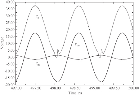
, Po = 7.5 W, and tuned circuit Q = 50. Then ![]() , C = 974 pF, L = 1.37 μH, VDD = 13.97 V, L0 = 59.68 μH, and C0 = 106.1 pF. The RF choke inductance was chosen to be 200 μH. Too small an inductance will allow ac currents to flow into the power supply. A SPICE analysis of this design is shown in Fig. 9.23 where the voltage across the switch, υ(θ), and the output voltage at the load, υo(θ), are displayed. The phase difference between the switch voltage and the load voltage shown in Fig. 9.23 is ϕ. The SPICE analysis is an approximation to the ideal circuit model, since convergence requirements determine that the switch have a nonzero on resistance and the switching time must be greater than zero.
, C = 974 pF, L = 1.37 μH, VDD = 13.97 V, L0 = 59.68 μH, and C0 = 106.1 pF. The RF choke inductance was chosen to be 200 μH. Too small an inductance will allow ac currents to flow into the power supply. A SPICE analysis of this design is shown in Fig. 9.23 where the voltage across the switch, υ(θ), and the output voltage at the load, υo(θ), are displayed. The phase difference between the switch voltage and the load voltage shown in Fig. 9.23 is ϕ. The SPICE analysis is an approximation to the ideal circuit model, since convergence requirements determine that the switch have a nonzero on resistance and the switching time must be greater than zero.
FIGURE 9.23 Voltage, υ(θ), at switch and the voltage, υo(θ) at the load. Phase difference between these two is ϕ.
The assumptions that this analysis was based on are (1) the device capacitance is considered to be independent of voltage amplitude, since it is linear, (2) the gate to drain capacitance, CGD is neglected, and (3) the load at harmonic frequencies is considered to be infinite. The latter could be enhanced by replacing the series-tuned circuit with a multipole filter. Another enhancement for the microwave frequency range is the use of two 45° transmission lines to provide the required shunt susceptance, B, while ensuring an open circuit at the output of the switch at the second-harmonic frequency [13]. This circuit provided a 0.94 W of output power with a drain efficiency of 75% at 1 GHz. Control of multiple harmonics leads to the class F amplifier described in the following section.
9.7 CLASS F POWER AMPLIFIER
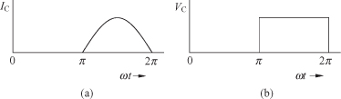
“A class F amplifier is characterized by a load network that has resonances at one or more harmonic frequencies as well as at the carrier frequency” [2, p. 454]. The class F amplifier was one of the early methods used to increase amplifier efficiency and has attracted some renewed interest recently. The circuit shown in Fig. 9.24 is a three-frequency peaking amplifier where the shunt resonator is resonant at the fundamental, f0, and the series resonator at 3f0. More details for higher order resonator class F amplifiers are found in [14]. When the transistor is excited by a sinusoidal source, ideally it is on for approximately half the time and off for half the time. The resulting output current waveform given in Fig. 9.25a is converted back to a sine wave by the resonator, L1, C1. The L3, C3 resonator is not quite transparent to the fundamental frequency, but blocks the frequency at 3f0 from getting to the load. The drain or collector voltage will range from 0 to twice the power supply voltage with an average value of VCC. The second harmonic voltage at 3f0 on the drain or collector, if it has the appropriate amplitude and phase, will tend to make this device voltage more square in shape. This will make the transistor act more like a switch with the attendant high efficiency.
FIGURE 9.24 Class F three-frequency peaking power amplifier.
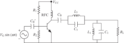
FIGURE 9.25 (a) Class F collector current and (b) ideal switching square wave.
9.7.1 Three-Frequency Peaking Class F Amplifier
The Fourier expansion of a square wave illustrated in Fig. 9.25b with amplitude from +1 to −1 and period 2π is
Consequently, to produce a square wave voltage waveform at the transistor terminal, the impedance must be a short at even harmonics and large at odd harmonics. Ordinarily, only the fundamental, first-harmonic and second-harmonic impedances are determined. In the typical class F amplifier shown in Fig. 9.24, the L1C1 tank circuit is resonant at the output frequency, f0, and the L3C3 tank circuit is resonant at 3f0. It has been pointed out [15] that the blocking capacitor, CB, could be used to provide a short to ground at 2f0 rather than simply acting as a dc block.
The design of the class F amplifier proceeds by first determining the output voltage from the desired output power and load resistance requirement. Of course, the load resistance can be transformed to a standard value by use of an impedance transformer. The resulting output voltage is
A square switching waveform at the collector can be approximated with the fundamental and two harmonics. Based on Eq. (9.157), the transistor collector voltage would be of the form
(9.159)
![]()
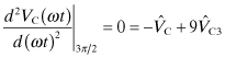
Setting the change of the slope to be zero at ωt = 3π/2 is done by
(9.160)
or
Furthermore, at ωt = π/2 the collector voltage is zero:
(9.162)
The expected maximum efficiency can be done much like the calculation done for the class B amplifier. The direct current for the class F amplifier is a half-wave-rectified current rather than a full-wave-rectified current. One might expect from the class B analysis that the direct current would be ![]() where
where ![]() is the voltage across the load. Since there is a short between the collector and the load at the fundamental,
is the voltage across the load. Since there is a short between the collector and the load at the fundamental, ![]() . For the class F amplifier the peak value of the load current is
. For the class F amplifier the peak value of the load current is ![]() . However, the current entering the blocking capacitor, CB, has a peak value of
. However, the current entering the blocking capacitor, CB, has a peak value of ![]() and a minimum value of zero. Thus, the average of the half wave current entering CB is
and a minimum value of zero. Thus, the average of the half wave current entering CB is
(9.163)
During the time the current is not flowing into the load through CB, it flows through the transistor to ground. The power from the supply is
and maximum power occurs for ![]() :
:
![]()
The maximum output power is
![]()
Thus, the maximum efficiency is
(9.164)
![]()
The determination of the reactive circuit begins by finding C1 from the desired amplifier bandwidth. The circuit Q is assumed to be determined solely by L1, C1, and RL. Thus,
![]()
or
Once C1 is determined, the inductance must be that which resonates the tank at f0:
At 2f0, the L1C1 tank circuit has negative reactance and the L3C3 tank circuit has positive reactance. The capacitances, CB and C3, can be set to provide a short to ground:
Since ![]() , and
, and ![]() , Eq. (9.167) reduces to
, Eq. (9.167) reduces to
![]()
or
which is the requirement for series resonance at 2f0. In addition, at the fundamental frequency, CB and the L3C3 tank circuit can be tuned to provide no reactance between the transistor and the load, RL. This eliminates the approximation that the L3C3 has zero reactance at the fundamental:
(9.169)
![]()
This value for CB can be substituted back into Eq. (9.168) to give a relationship between C3 and C1:
In summary, C1 is determined by the bandwidth Eq. (9.165), L1 by Eq. (9.166), C3 from Eq. (9.171), L3 from its requirement to resonate C3 at 3f0, and finally CB from Eq. (9.170). In addition, interstage networks are presented in [15] that aim at reducing the spread in circuit element values and hence help make circuit design practical.
As a numerical example, an amplifier is to be designed to deliver 10 W of power to a 25-Ω load at 900 MHz. From (9.158), ![]() and using Eq. (9.161) the required dc supply voltage is 19.87 V, so VCC = 20 V is chosen. Knowledge of
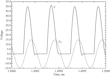
and using Eq. (9.161) the required dc supply voltage is 19.87 V, so VCC = 20 V is chosen. Knowledge of ![]() gives the direct current from the power supply as Idc = 569.4 mA from Pdc/VCC. Assume the desired bandwidth requires Q = 100. Then C1 = 707.35 pF, L1 = 44.21 pH, C3 = 358.10 pF, L3 = 9.70 pH, and CB = 2.86 nF. A SPICE analysis using the default SPICE bipolar transistor model gives the collector current (Fig. 9.26) and the voltages at the collector and load (Fig. 9.27). Since actual transistor models are much more complicated than that used here, actual results could be quite different from those shown.
gives the direct current from the power supply as Idc = 569.4 mA from Pdc/VCC. Assume the desired bandwidth requires Q = 100. Then C1 = 707.35 pF, L1 = 44.21 pH, C3 = 358.10 pF, L3 = 9.70 pH, and CB = 2.86 nF. A SPICE analysis using the default SPICE bipolar transistor model gives the collector current (Fig. 9.26) and the voltages at the collector and load (Fig. 9.27). Since actual transistor models are much more complicated than that used here, actual results could be quite different from those shown.
FIGURE 9.26 SPICE simulation of collector current of class F amplifier.
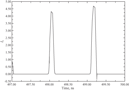
FIGURE 9.27 SPICE simulation of collector and load voltages of class F amplifier.
9.7.2 Transmission Line Class F Amplifier
Additional odd harmonics can be controlled by adding additional resonators that make the collector voltage come closer to having a square shape. In effect, an infinite number of odd harmonic resonators can be added if a λ/4 transmission line at the fundamental frequency replaces the lumped-element L3C3 second-harmonic resonator (Fig. 9.28).
FIGURE 9.28 Class F transmission line power amplifier.
The admittance at the fundamental frequency seen by the collector is
(9.172)
![]()
The λ/4 transmission line converts the shunt load at the end of the line to an effective series load at the collector:
(9.173)
![]()
in which
![]()
![]()
![]()
At the first harmonic, the transmission line is λ/2 and the resonator (L1, C1 ) is a short, so ![]() . The effective load for all the harmonics can be found easily at each of the harmonics:
. The effective load for all the harmonics can be found easily at each of the harmonics:
![]()
![]()
![]()
![]()
While this provides open and short circuits to the collector, it is not obvious that these impedances, which act in parallel with the output impedance of the transistor, will provide the necessary amplitude and phase that would produce a square wave at the collector.
There are some practical difficulties in trying to make the transmission line class F amplifier. Most obvious is the physical size of a λ/4 line. For typical radio frequencies a technique would need to be used to make the line mechanically short while still providing an electrical length of π/2 at the fundamental operating frequency. Furthermore, the resonator capacitance, C1, must be sufficiently large to provide approximately zero reactance at 2fo. At the same time the desired bandwidth also governs the size of C1 [Eq. (9.165)]. The competing requirements of low second-harmonic impedance and the desired Q may produce an unacceptable compromise. A more extensive harmonic balance analysis of a physics-based model for a metal semiconductor field-effect transistor (MESFET) showed that a power added efficiency of 75% can be achieved at 5 GHz [16].
9.8 FEED-FORWARD AMPLIFIERS
The concept of feed-forward error control was conceived in a patent disclosure by Harold S. Black in 1924 [17]. This was several years prior to his more famous concept of feedback error control. A historical perspective on the feed-forward idea is found in [18]. The feedback approach is an attempt to correct an error after it has occurred. However, a 180° phase difference in the forward and reverse paths in a feedback system can cause unwanted oscillations. In contrast, the feed-forward design is based on cancellation of amplifier errors in the same time frame in which they occur. Signals are handled by wide-band analog circuits, so multiple carriers in a signal can be controlled simultaneously. Feed-forward amplifiers are inherently stable, but this comes at the price of a somewhat more complicated circuit. Consequently, feed-forward circuitry is sensitive to changes in ambient temperature, input power level, and supply voltage variation. Nevertheless feed-forward design offers many advantages that have brought increased interest.
The major source of distortion, such as harmonics, intermodulation distortion, and noise, in a transmitter is the power amplifier. This distortion can be greatly reduced using a feed-forward design. The basic idea is illustrated in Fig. 9.29 where it is seen that the circuit consists basically of two loops. The first one contains the main power amplifier, and the second loop contains the error amplifier. In the first loop, a sample of the input signal is coupled through coup1 reducing the signal by the coupling factor −C1 dB. This goes through the delay line with insertion loss of −D1 dB into the comparator coupler coup3. At the same time the signal passing through the main amplifier with gain G1 dB is sampled by coupler coup2, reducing the signal by −C2 dB, the attenuator by −L1 dB, and the coupler coup3 by −C3 dB. The delay line, delay1, is adjusted to compensate for the time delay in the main amplifier as well as the passive components so that two input signals for coup3 are 180° out of phase but synchronized in time. The amplitude of the input signal when it arrives at the error amplifier is
(9.174)
![]()
FIGURE 9.29 Linear feed-forward amplifier.
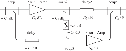
which should be adjusted to be zero. What remains is the distortion and noise added by the main amplifier, which is in turn amplified by the error amplifier by G2 dB. At the same time the signal from the main amplifier with its distortion and noise is attenuated by D2 dB in the second loop delay line. The second delay line is adjusted to compensate for the time delay in the error amplifier. The relative phase and amplitude of the input signals to coup4 are adjusted so that the distortion terms cancel. The output distortion amplitude
![]()
should be zero for complete cancellation to occur.
The error amplifier will also add distortion and noise to its input signal so that perfect error correction will not occur. Nevertheless, a dramatic improvement is possible since the error amplifier will be operating on a smaller signal (only distortion) that will likely lie in the linear range of the amplifier. Further improvement may be accomplished by treating the entire amplifier in Fig. 9.29 as the main amplifier and adding another error amplifier with its associated circuitry [18].
A typical implementation of a feed-forward system is described in [19] for an amplifier operating in the frequency range of 2.1 to 2.3 GHz with an RF gain of 30 dB and an output power of 1.25 W. This amplifier had intermodulation products at least 50 dB below the carrier level. Their design used a 6-dB coupler for coup1, a 13-dB coupler for coup2, a 10-dB coupler for coup3, and an 8-dB coupler for coup4. In some designs, the comparator coupler, coup3, is replaced by a power combiner.
The directional coupler itself can be implemented using microstrip or stripline coupled lines at higher frequencies [20] or by a transmission line transformer like that shown in Fig. 6.17. A variety of feed-forward designs have been implemented, some using digital techniques [21, 22].
9.9 CONCLUSIONS
The discussion in this chapter has centered on two basic types of power amplifiers: the linear class A, AB, and B amplifiers and the nonlinear class C, D, E, and F amplifiers. The alphabet soup of power amplifiers does continue beyond class F, but these are the most widely used types today. In general, though, higher efficiency comes with the cost of higher distortion. The feed-forward amplifier does attempt to reduce noise and distortion by cancellation, but with the cost of higher complexity and some loss in efficiency. The Doherty power amplifier, though not discussed in this chapter, represents a technique of using two parallel amplifiers where the auxiliary amplifier provides additional current when the main amplifier begins to saturate at high signal level. It is an attempt to provide high efficiency while maintaining signal integrity.
PROBLEMS
9.1. If the crossover discontinuity is neglected, is a class B amplifier considered a linear amplifier or a nonlinear amplifier. Explain your answer.
9.2. A class B amplifier such as that shown in Fig. 9.7 is biased with an 18-V power supply, but the maximum voltage amplitude across each transistor is 16 V. The remaining 2 V is dissipated as loss in the output transformer. If the amplifier is designed to deliver 12 W of RF power, what is
a. The maximum RF collector current?
b. The total dc current from the power supply?
c. The collector efficiency of this amplifier?
9.3. The bipolar class C amplifier equivalent to that shown in Fig. 9.9 has a conduction angle of 60°. It is designed to deliver 75 W of RF output power. The saturated collector–emitter voltage is known to be 1 V and the power supply voltage is 26 V. What is the maximum peak collector current?
9.4. Assume the class C amplifier shown in Fig. 9.9 is excited by the rectangular wave shown in Fig. 9.30. Determine the efficiency of this amplifier as a function of ψ. If the conduction angle 2ψ = π/3, what is the numerical value for the efficiency?
FIGURE 9.30 Square wave pattern for Problem 9.4.
9.5. A class C amplifier is to be designed using a bipolar transistor to produce a maximum average output power, Po = 26 W, at 50 MHz. The transistor being used has a saturation voltage, VCE−sat = 2 V. The power supply voltage is VCC = 28 V. The current wave form shown in Fig. 9.10 can be used where IQ = −4 A, ![]() , and ψ = 45°.
, and ψ = 45°.
a. Determine, r, the ratio of the average power to the peak power.
b. Determine the load resistance needed to realize the required output power.
9.6. A certain power amplifier in the common emitter configuration has a conduction angle of 120°. What is the class type (A, AB, B, C, …) of the amplifier in Fig. 9.31? The maximum average power delivered to the load by this amplifier is 30 W. What is the peak instantaneous power across the output terminals?
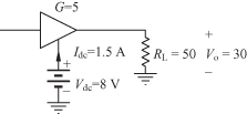
FIGURE 9.31 Amplifier used to determine power efficiency in Problem 9.7.
REFERENCES
1. P. R. Gray, P. J. Hurst, S. H. Lewis, and R. G. Meyer, Analysis and Design of Analog Integrated Circuits, New York: Wiley, 2001.
2. H. L. Krauss, C. W. Bostian, and F. H. Raab, Solid State Radio Engineering, New York: Wiley, 1980.
3. W. L. Everitt, “Optimum Operating Conditions for Class C Amplifiers,” Proc. Inst. Radio Eng., 22, pp. 152–176, Feb. 1934.
4. D. M. Snider, “A Theoretical Analysis and Experimental Confirmation of the Optimum Loaded and Overdrive RF Power Amplifier,” IEEE Trans. Electron Devices, ED-14, pp. 851–857, Dec. 1967.
5. H. Kobayashi, J. M. Hinrichs, and P. M. Asbeck, “Current-Mode Class-D Amplifiers for High-Efficiency RF Applications,” IEEE Trans. Microwave Theory Tech., 49, pp. 2480–2485, December 2001.
6. A. L. Long, High Frequency Current Mode Class-D Amplifiers with High Output Power and Efficiency, ECE Technical Report #03-XX, M.S. Thesis, Dept. of Electrical and Computer Engineering, University of California, Santa Barbara, May 2003.
7. G. D. Ewing, High-Efficiency Radio-Frequency Power Amplifiers, Ph.D. Dissertation, Oregon State University, Corvallis, OR, April 1964.
8. N. O. Sokal and A. D. Sokal, “Class E—A New Class of High-Efficiency Tuned Single-Ended Power Amplifiers,” IEEE J. Solid State Circuits, SC-10(3), pp. 168–176, June 1975.
9. F. H. Raab, “Idealized Operation of the Class-E Tuned Power Amplifier,” IEEE Trans. Circuits Syst., CAS-24(12), pp. 725–735, Dec. 1977.
10. F. H. Raab, “Effects of Circuit Variations on the Class-E Tuned Power Amplifier,” IEEE J. Solid State Circuits, SC-13(2), pp. 239–247, April 1978.
11. W. H. Cantrell, “Tuning Analysis for the High-Q Class-E Power Amplifier,” IEEE Trans. Microwave Theory Tech., 48(12), pp. 2397–2402, Dec. 2000.
12. W. H. Cantrell, Analysis of High-Q Class-E Power Amplifier, Rectifier and Ampli tude Modulator, Ph.D. Dissertation, University of Texas Arlington, Arlington, TX, December, 2002.
13. T. B. Mader and Z. B. Popovic, “The Transmission-Line High-Efficiency Class-E Amplifier,” IEEE Microwave Guided Wave Lett., 5, pp. 290–292. Sept. 1995.
14. F. H. Raab, “Class-F Power Amplifiers with Maximally Flat Waveforms,” IEEE Trans. Microwave Theory Tech., Vol. 45, pp. 2007–2012, Nov. 1997.
15. C. Trask, “Class-F Amplifier Loading Networks: A Unified Design Approach,” 1999 IEEE MTT-S International Symposium Digest, Piscataway, NJ: IEEE Press, pp. 351–354, 1999.
16. L. C. Hall and R. J. Trew, “Maximum Efficiency Tuning of Microwave Amplifiers,” 1991 MTT-S International Symposium Digest, Piscataway, NJ: IEEE Press, pp. 123–126, 1991.
17. H. S. Black, U.S. Patent 1,686,792, issued Oct. 9, 1929.
18. H. Seidel, H. R. Beurrier, and A. N. Friedman, “Error-Controlled High Power Linear Amplifiers at VHF,” Bell Syst. Tech. J., 47, pp. 651–722, May–June 1968.
19. C. Hsieh and S. Chan, “A Feedforward S-Band MIC Amplifier System,” IEEE J. Solid State Circuits, SC-11, pp. 271–278, April 1976.
20. W. A. Davis, Microwave Semiconductor Circuit Design, Chapter 4, New York: Van Nostrand, 1984.
21. S. J. Grant, J. K. Cavers, and P. A. Goud, “A DSP Controlled Adaptive Feed Forward Amplifier Linearizer,” Annual International Conference on Universal Personal Communications,, pp. 788–792, Cambridge, Ma: Sept. 29–Oct. 2 1996.
22. G. Zhao, F. M. Channouchi, F. Beauregard, and A. B. Kouki, “Digital Implementations of Adaptive Feedforward Amplifier Linearization Techniques,” IEEE Microwave Theory Tech. Symp. Digest, June 1996.