
CHAPTER SEVEN
Noise in RF Amplifiers
7.1 SOURCES OF NOISE
The dynamic range of a communication transmitter or receiver circuit is usually limited at the high-power point by nonlinearities and at the low-power point by noise. Noise is the random fluctuation of electrical power that interferes with the desired signal. There can be interference with the desired signal by other unwanted deterministic signals, but at this point only the interference caused by random fluctuations will be considered. There are a variety of physical mechanisms that account for noise, but probably the most common source is thermal (also referred to as Johnson noise or Nyquist noise). This can be illustrated by simply examining the voltage across an open-circuited resistor (Fig. 7.1). The resulting voltage is not zero! The average voltage is zero but not the instantaneous voltage. At any temperature above absolute 0 K the Brownian motion of the electrons will produce random instantaneous currents. These currents will produce random instantaneous voltages, and this leads to noise power.
FIGURE 7.1 Voltage across open-circuit resistor.
Noise arising in electron tubes, semiconductor diodes, bipolar transistors, or field-effect transistors come from a variety of mechanisms. For example, for tubes, these include random times of emission of electrons from a cathode (called shot noise), random electron velocities in the vacuum, nonuniform emission energy over the surface of the cathode, and secondary emission from the anode. Similarly for diodes, a random emission of electrons and holes produces noise. In a bipolar transistor, in addition to the diode noise there is partition noise. This represents the fluctuation in the path that charge carriers take through the base to the collector after leaving the emitter. There is in addition 1/f or flicker noise (where f is frequency), which is probably caused by surface recombination of base minority carriers at the base–emitter junction [1]. Clearly, as the frequency approaches dc, the flicker noise increases dramatically. As a consequence, intermediate-frequency amplifier stages in transceivers are designed to operate well above the frequency where 1/f noise is a significant contributor to the total noise. Typically, the 1/f noise is significant in the frequency ranges from 100 Hz to 10 kHz. In a field-effect transistor, there is thermal noise arising from channel resistance, 1/f noise, and a coupling of the channel noise back to the gate where it is, of course, amplified by the transistor gain. Noise also arises from reverse breakdown in the avalanching of electrons in such devices as Zener diodes and IMPATT diodes. At radio frequencies, the two most common noise sources are the thermal noise and the shot noise.
7.2 THERMAL NOISE
The random fluctuation of electrons in a resistance would be expected to rise as the temperature increases since the electron velocities and the number of collisions per second increases. The mean-square noise voltage is expressed as an autocorrelation of the instantaneous voltage over a time period T:
(7.1)
![]()
The expression for the thermal noise voltage has been derived in a variety of ways. Harry Nyquist first solved the problem based on a transmission line model. Other approaches included using a lumped-element circuit, the random motion of electrons in a metal conductor, or the radiation from a black body. These are all basically thermodynamic models and each method results in the same expression. The black-body method is based on quantum mechanics and therefore provides a solution for noise sources at both cryogenic and room temperatures.
7.2.1 Black-Body Radiation
Classical mechanics is based on the continuity of energy states. When this theory was applied to calculation of the black-body radiation, it was found that the radiation increased without limit. This so-called ultraviolet catastrophe was clearly not physical. However, Planck was able to correct the situation by postulating that energy states are not continuous but are quantized in discrete states. These energy values are obtained by solving the Schrödinger equation for the harmonic oscillator. The actual derivation is found in most introductory texts on quantum mechanics [2]:
(7.2)
![]()
In this equation h = 6.547 × 10⁻³⁴ J·s is Planck’s constant. If energy were continuous, then the average energy could be obtained from the Boltzmann probability distribution function, P(ε), by the following integral:
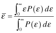
where
(7.4)
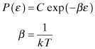
and
![]()
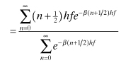
The value, k = 1.380 × 10⁻²³ J/K, is the Boltzmann constant and is essentially the proportionality constant between energy measured in terms of joules and energy measured in terms of absolute temperature. Planck replaced the continuous integrals in Eq. (7.3) with summations of the discrete energy levels [3]:
(7.5)

(7.6)
It may be easily verified by differentiation that
The argument of the logarithm can be evaluated by recognizing it as an infinite geometric series:
If Eq. (7.8) is substituted back into Eq. (7.7), the average energy can be found:
(7.9)
or
This will be used as the starting point for finding the noise power.
7.2.2 Nyquist Formula
The thermal noise power in a given bandwidth, Δf, is obtained directly from Eq. (7.10):
At room temperature the second term, hf Δf/2, plays no role, but it may be essential in finding the minimum noise figure for cryogenically cooled devices [4]. An approximation for the noise power can be found by expanding Eq. (7.11) into a Taylor series:
(7.12)
![]()
At room temperature, hf/kT
![]() 1, so
that this reduces to the usual practical formula for noise power as given by Nyquist
[5]:
1, so
that this reduces to the usual practical formula for noise power as given by Nyquist
[5]:
(7.13)
![]()
If this is the available power, the corresponding mean-squared voltage is obtained by multiplying this by four times the resistance, R:
The mean-squared noise current is
(7.15)
![]()
where G is the associated conductance.
7.3 SHOT NOISE
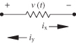
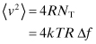
Shot noise arises from random variations of a direct current, I0, and is especially associated with current-carrying active devices. Shot noise is most apparent in a current source with zero shunt source admittance. For the purpose of illustration, consider a current source feeding a parallel RLC circuit (Fig. 7.2). The inductor provides a dc path and is open to ac variations of the current. Hence, the resulting noise voltage appears across the resistor (which is presumed free of any thermal noise). If an instrument could measure the current produced by randomly arriving electrons, the instrument would record a series of current impulses for each electron. If n is the average number of electrons emitted by the source in a given time interval Δt, then the dc current is
where q is the charge of an electron. Each current pulse provides an energy pulse to the capacitor with the value of
FIGURE 7.2 Equivalent circuit for shot noise and for certain thermal noise calculations.
The average shot noise power delivered to the load is then
![]()
which in the light of Eqs. (7.16) and (7.17) becomes

The equipartition theorem as found in thermodynamics books states that the average energy of a system of uniform temperature is equally divided among the degrees of freedom of the system. If there are N degrees of freedom, then
(7.19)
![]()
A system with N degrees of freedom can be described uniquely by N variables. The circuit in Fig. 7.2 has two energy storage elements, each containing an average energy of kT/2. For the capacitor this average energy is
(7.20)
![]()
But, it was found that the Nyquist noise formula predicted that 〈v2〉 = 4kTR Δf. Consequently,
Using Eq. (7.21) to replace the value of the capacitance in Eq. (7.18) gives the desired formula for the shot noise power:
(7.22)
![]()
The corresponding shot noise current is found by dividing by R
(7.23)
![]()
The shot noise current is directly proportional to the direct current as has been verified experimentally.
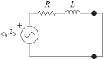
7.4 NOISE CIRCUIT ANALYSIS
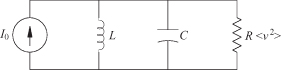
When a circuit contains several resistors, the total noise power can be calculated by suitable combination of the resistors. Two resistors in series each produce a mean-squared voltage, 〈v2〉. Since the individual noise voltage sources are uncorrelated, the total 〈v2〉 is the sum of the 〈v2〉 of each of the two resistors. Similarly, two conductances in parallel each produce a mean-squared noise current, 〈i2〉, that may be added when the two conductances are combined since the noise currents are uncorrelated. It should be emphasized that two noise voltages 〈v〉 cannot be added together; only the mean-square values can be added. The use of an arrow in the symbol for a noise current source is used to emphasize that this is a current source. The use of + and − signs in the symbol for a noise voltage source are used to emphasize that this is a voltage source. They do not imply anything about the phase of the noise sources. When both series and parallel resistors are present as shown in Fig. 7.3, then Thévenin’s theorem provides an equivalent circuit and associated noise voltage. In Fig. 7.3 the output resistance is (R1 + R2) || R3, and the corresponding noise voltage delivered to the output is
(7.24)
![]()
FIGURE 7.3 Noise voltage from series and parallel resistors.
When there is a reactive element in the circuit such as that shown in
the simple RLC circuit in Fig. 7.4, the output noise voltage would be attenuated by the
magnitude of the total admittance. Typically, the the measured noise frequency,
f, is approximately a sinusoid, which occurs when
f
![]() Δf. Then
Δf. Then
(7.25)
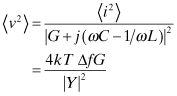
FIGURE 7.4 Noise voltage from RLC circuit.
If the output resistance varies appreciably over the range of the noise bandwidth Δf, then the individual noise “sinusoids” must be summed over the bandwidth, resulting in the following integral:
(7.26)
![]()
As a simple example, consider the noise generated from a shunt RC circuit that would result from removing the inductance in Fig. 7.4:
(7.27)
![]()
This expression does not say that the capacitor is the source of the noise voltage. Indeed experiments have shown that changing the temperature of the resistor is what changes the output noise. When the 3-dB frequency point of the circuit output impedance [f3dB = 1/(2πRC)] is considered, the noise voltage in Eq. (7.28) becomes
![]()
This looks similar to the original Nyquist formula [Eq. (7.14)] in its form.
7.5 AMPLIFIER NOISE CHARACTERIZATION
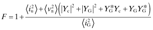
One important quality factor of an amplifier is a measure of how much noise it adds to the signal while it amplifies it. The “actual noise factor,” F, is a convenient measure of how the amplifier affects the total output noise. The definition of noise factor from the Institute of Electrical and Electronic Engineers (IEEE) standards is the ratio of (1) the total noise power per unit bandwidth at a corresponding output port when the noise temperature of the input termination is standard 290 K to (2) that portion of the total noise power engendered at the input frequency by the input termination [6]. The standard T0 = 290 K noise temperature approximates the actual noise temperature of most input terminations:
(7.29)
In this expression GT is the transducer power gain. Noise factor is a measure of the total output noise after it leaves the amplifier divided by the input noise power entering the amplifier and amplified by an ideal noiseless gain, GT. In an analog amplifier, an amplifier can only add noise so F must always be greater than 1. The noise factor can also be expressed in terms of the signal-to-noise ratio at the input to that at the output. If P represents the input signal power, then
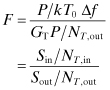
The signal-to-noise ratio will always be degraded as the signal goes through the amplifier. The expression Eq. (7.30) is strictly true only if the input temperature is 290 K. This is called the spot noise factor.
The portion of the total thermal noise output power contributed by the amplifier itself is
(7.31)
![]()
(7.32)
![]()
The factor (F − 1) is used in two alternative measures of noise. One of these is noise temperature, which is particularly useful when dealing with very low noise amplifiers where the decibel scale typically used in describing noise figure becomes too compressed to give insight. In this case, the equivalent noise temperature is defined as
(7.33)
![]()
This is the temperature of the source resistance that when connected to the noise-free two-port circuit will give the same output noise as the original noisy circuit.
Another useful parameter for the description of noise is the noise measure [7]:
(7.34)
![]()
This is particularly useful for optimizing a receiver in which, for example, a trade-off has to be made between a low-gain low-noise amplifier and a high-gain high-noise amplifier.
7.6 NOISE MEASUREMENT
Measurement of noise figure (noise factor measured in decibels) can be accomplished by using a power meter and determining the circuit bandwidth and gain. However, it is inconvenient to determine gain and bandwidth each time a noise measurement is to be taken. The Y factor method for determining noise factor is an approach where these two quantities need not be determined explicitly. Actual noise measurements are done over a range of frequencies. The average noise factor over a given bandwidth is [6]
(7.35)
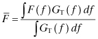
This represents a more realistic expression for an actual noise measurement than the spot noise factor such as in Eq. (7.30).
An equivalent noise bandwidth Δf0 can be defined in terms of the maximum gain over the band as
(7.36)
![]()
so that
(7.37)
![]()
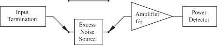
A measurement system that can be used to measure the noise factor of an amplifier is shown in Fig. 7.5. This excess noise source in this circuit is gated on and off to produce two values of noise measured at the output power detector, N1 and N2.
Nex = calibrated excess noise source at T2 − T0
N1 = NT,out when excess noise source is off
N2 = NT,out when excess noise source is on
Nin = noise from input termination
Na = noise added by the amplifier itself
FIGURE 7.5 Noise measurement using Y factor method.
The Y factor as the ratio of N2 to N1 is easily obtained:
(7.38)
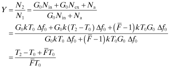
When solved for ![]()
(7.39)
![]()
Since a calibrated noise source is used, (T2 − T0)/T0 is known. Also Y is known from the measurement. The amplifier noise factor is then obtained.
7.7 NOISY TWO-PORT CIRCUITS
The noise delivered to the output of a two-port circuit depends on the two-port circuit itself and the impedance of the input excitation source. The noise factor for a two-port circuit is given by the following:
| where Fmin = minimum noise factor |
| R n = equivalent noise resistance (often device data are given in terms of a normalized resistance, rn = Rn/50) |
| Y G = GG + jBG excitation source admittance |
| Y opt = Gopt + jBopt optimum source admittance where the minimum noise factor occurs |
While a designer can choose YG to minimize the noise factor, such a choice will usually reduce the gain somewhat. Sometimes the noise factor is expressed in terms of the reflection coefficient at the input:
(7.41)
![]()
where Y0 and Z0 are the characteristic admittance and impedance, respectively. Then the noise factor is
(7.42)
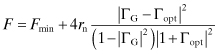
The noise factor expression in Eq. (7.40) and its equivalent (7.42) are the basic expressions used to optimize transistor amplifiers for noise figure. The derivation of Eq. (7.40) is the subject of the following section. Readers not wishing to pursue these details at this point may proceed to Section 7.9 without loss of continuity.
7.8 TWO-PORT NOISE FACTOR DERIVATION
The work described here is based on the Institute of Radio Engineers (IRE) standards published between 1956 and 1960 [8, 9]. A noisy resistor can be modeled as a noiseless resistor in series with a voltage noise source. In similar fashion a two-port circuit can be represented as a noiseless two-port and two noise sources. These two noise sources are represented in Fig. 7.6a as a voltage vn and a current in. The two-port circuit can be described in terms of its ABCD parameters and internal noise sources as
(7.43)
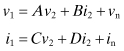
FIGURE 7.6 Equivalent circuit (a) for two-port noise calculation and (b) equivalent Thévenin circuit.
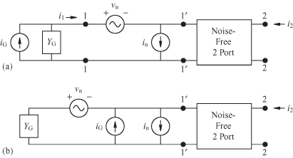
or as shown in Fig. 7.6 as a noiseless circuit and the noise sources referred to the input side. If the input termination, YG, produces a noise current, iG, then the circuit is completed. The polarity markings on the symbols for the noise sources merely point out the distinction between voltage and current sources. Being noise sources, the polarities are actually random. The Thévenin equivalent circuit in Fig. 7.6b shows that the short-circuit current at the 1′ − 1′ port is
(7.44)
![]()
The total output noise power is proportional to ![]() , and the noise caused by the input
termination source alone is
, and the noise caused by the input
termination source alone is ![]() . The
noise-free part between 1′ − 1′ and 2 − 2 is noise free; that is, it adds no
additional noise to the output. All the noise sources are referred to the input side
so that the noise factor is
. The
noise-free part between 1′ − 1′ and 2 − 2 is noise free; that is, it adds no
additional noise to the output. All the noise sources are referred to the input side
so that the noise factor is

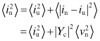
Part of the noise current source, in, is correlated and part is uncorrelated with the noise voltage vn. The uncorrelated current is iu. The rest of the current is correlated with vn and is given by in − iu. This correlated noise current must be proportional to vn. The proportionality constant is the correlation admittance given by Yc = Gc + jBc and is defined so that
While this defines Yc, its explicit value in the end will not be needed. The mean value of the product of the correlated and uncorrelated current is, of course, 0. By definition, the average of the product of the noise voltage, vn, and the uncorrelated noise current, iu, must also be 0. Using the complex conjugate of the current (which is a fixed phase shift) will not change this fact:
Rearranging Eq. (7.47) gives
The product of the noise voltage and the uncorrelated current in Eq. (7.48) can be expressed by substitution of Eq. (7.49) into Eq. (7.48):
(7.50)
![]()
Because ![]() from Eq. (7.48), the product of the noise
voltage and the correlated current can be found using Eq. (7.47):
from Eq. (7.48), the product of the noise
voltage and the correlated current can be found using Eq. (7.47):
The noise source values are determined by their corresponding resistances:
(7.52)
![]()
(7.53)
![]()
(7.54)
![]()
The resistance, Rn, is the
equivalent noise resistance for ![]() , and
Gu is the equivalent noise conductance
for the uncorrelated part of the noise current,
, and
Gu is the equivalent noise conductance
for the uncorrelated part of the noise current, ![]() . The total noise current is the sum of the uncorrelated current
and the remaining correlated current:
. The total noise current is the sum of the uncorrelated current
and the remaining correlated current:
(7.56)
![]()
The expression for the short-circuit current in Eq. (7.45) can be modified by Eq. (7.51):
(7.57)
![]()
Furthermore, ![]() can be
replaced by Eq. (7.55).
can be
replaced by Eq. (7.55).
(7.58)
![]()
The noise factor, given by Eq. (7.46), can now be put in more convenient form:
(7.59)
(7.60)
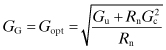
The value of F is a function of the input termination admittance, YG, and reaches a minimum when the source admittance is optimum. In particular, the optimum susceptance is BG = Bopt = −Bc. The value for Fmin is found by setting the derivative of F with respect to GG to zero and setting BG = −Bc. This will determine the value for GG = Gopt in terms of Gu, Ru, and Gc:
(7.62)
![]()
Solution for GG yields
(7.63)
or
Substituting this into Eq. (7.61) (with susceptance BG + Bc = 0) provides the minimum noise factor, Fmin:
(7.65)
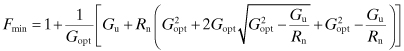
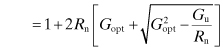
The correlation conductance, Gc of Eq. (7.64) is substituted into the total noise factor expression of Eq. (7.61) to give
(7.67)
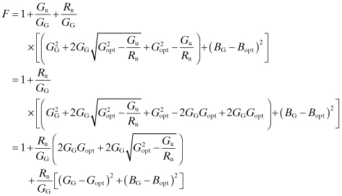
The first two terms are the same as Fmin in Eq. (7.66), so
(7.68)
![]()
7.9 FUKUI NOISE MODEL FOR TRANSISTORS
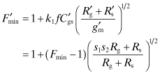
Fukui found an empirically based model that accurately describes the frequency dependence of the noise for high-frequency field-effect transistors [10]. This model reduces to predicting the four noise parameters, Fmin, Rn, Ropt, and Xopt where the latter two parameters are formed from the reciprocal of Yopt. For the circuit shown in Fig. 7.7, the Fukui relationships are as follows:
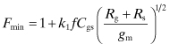
(7.70)
![]()
FIGURE 7.7 Equivalent circuit for noise calculation for FET.
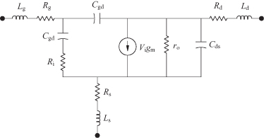
In these expressions, f is the operating frequency in gigahertz, the capacitance is in picofarads, and the transconductance in siemens. The constants k1, k2, k3, and k4 are empirically based fitting factors. The expression for Ropt in Eq. (7.71) differs from that originally given by Fukui, as modified by Golio [11]. The circuit elements of the equivalent FET model in Fig. 7.7 can be extracted at a particular bias level. The resistance, Ri, is often difficult to obtain, but for purposes of the noise estimation, it may be incorporated with the Rg. The empirically derived fitting factors should be independent of frequency. They are not quite constant, but over a range of 2 to 18 GHz average values for these are shown below [11]:
![]()
![]()
![]()
![]()
These values can be used for approximate estimates of noise factor for both metal semiconductor field-effect transistors (MESFETs) as well as high electron mobility transistors (HEMTs).
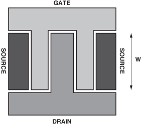
The transistor itself can be modified to provide either improved noise characteristics or improved power handling capability by adjusting the gate width W. The drain current, Ids, increases with the base width W. Consequently, those equivalent circuit parameters determined by derivatives of Ids will also be proportional to W. Also the capacitance between the gate electrode and the source electrode or between the gate electrode and the drain electrode will be also proportional to W. This is readily seen from the layout of a FET shown in Fig. 7.8. The gate resistance, Rg, scales differently since the gate current flows in the direction of the width. Also, the number of gate fingers, N, will reduce the effective gate resistance. The gate resistance is then proportional to W/N [12]. These relationships may be summarized as follows:
![]()
![]()
![]()
![]()
![]()
FIGURE 7.8 Typical FET layout.
These circuit elements can clearly be adjusted by scaling the transistor geometry. This scaling will in turn change the noise characteristics. If a transistor with a given geometry has a known set of noise parameters, then the noise characteristics of a new modified transistor can be predicted. The scaling factors between the new and the old transistor are
(7.73)
![]()
(7.74)
![]()
As a result, the new equivalent circuit parameters can be predicted [11]:
(7.75)
![]()
(7.76)
![]()
(7.77)
![]()
(7.78)
![]()
(7.79)
![]()
The Fukui equations, (7.69) to (7.72), for the newly scaled equivalent circuit parameters are
(7.81)
![]()
(7.82)
![]()
Reference should be made to [11] for a much fuller treatment of modeling MESFETs and HEMTs.
A further refinement in the calculation of drain noise current resulting from an N finger gate resistance, each of value Rg/N, was given in [13]. The total drain noise current is found to be
(7.84)
![]()
and if N → ∞
(7.85)
![]()
The bipolar transistor has a much different variation of noise with frequency than does the FET type of device. An approximate value for Fmin for the bipolar transistor at high frequencies is [14]
where
(7.87)
![]()
In this equation, Ic is the dc collector current, rb is the base resistance, and ωT is the frequency where the short-circuit current gain is 1. Values for Yopt and Rn are also given in [14], but are rather lengthy. A somewhat more accurate expression is given in [15].
Comparison of Eq. (7.86) with the corresponding expression for FETs, Eq. (7.69), indicates that the bipolar transistor minimum noise factor increases with f2, while that for the FET it increases only as f. Consequently, designs of low-noise amplifiers at RF and microwave frequencies would tend to favor use of FETs.
PROBLEMS
7.1. Determine the noise power at T = 290 K, f = 10 GHz, and Δf = 1 Hz. Determine the noise power at liquid helium temperature (4 K). What is the value of the error if the standard Nyquist formula is used?
7.2. What is the noise current from a noise voltage source in a series RL circuit shown in Fig. 7.9?
FIGURE 7.9 Noise current developed by series RL circuit.
7.3. Derive Eqs. (7.80) to (7.83).
7.4. A MESFET has a base width W = 350 µm and at 3 GHz with a
given bias is found to have gm = 70 mS, Rg = 5 ![]() , Rd = 7
, Rd = 7 ![]() , Rs = 5
, Rs = 5 ![]() , and
Cgs = 0.3 pF. What are the four noise
parameters Fmin, Rn, Ropt, and Xopt? If the base width is changed to W′ = 200 µm and the number of
base fingers remains unchanged, what are the four noise parameters?
, and
Cgs = 0.3 pF. What are the four noise
parameters Fmin, Rn, Ropt, and Xopt? If the base width is changed to W′ = 200 µm and the number of
base fingers remains unchanged, what are the four noise parameters?
REFERENCES
1. J. L. Plumb and E. R. Chenette, “Flicker Noise in Transistors,” IEEE Trans. Electron Devices, ED-10, pp. 304–308, Sept. 1963.
2. A. Messiah, Quantum Mechanics, Amsterdam: North-Holland, Chapter 12, 1964.
3. W. A. Davis, Microwave Semiconductor Circuit Design, New York: Van Nostrand, Chapters 8 and 9, 1984.
4. A. E. Siegman, “Zero-Point Energy as the Source of Amplifier Noise,” Proc. IRE, 49, pp. 633–634, March 1961.
5. H. Nyquist, “Thermal Agitation of Electronic Charge in Conductors,” Phys. Rev., 32, p. 110, July 1928.
6. H. A. Haus, “IRE Standards on Methods of Measuring Noise in Linear Twoports,” Proc. IRE, 47, pp. 66–68, Jan. 1959.
7. K. Kurokawa, “Actual Noise Measure of Linear Amplifiers,” Proc. IRE, 49, pp. 1391–1397, March 1961.
8. H. Rohte and W. Danlke, “Theory of Noisy Fourpoles,” Proc. IRE, 44, pp. 811–818, June 1956.
9. H. A. Haus, “Representation of Noise in Linear Twoports,” Proc. IRE, 48, pp. 69–74, Jan. 1960.
10. H. Fukui, “Design of Microwave GaAs MESFETs for Broad-Band Low-Noise Amplifiers,” IEEE Trans. Electron Devices, ED-26, pp. 1032–1037, July 1979.
11. J. M. Golio, Microwave MESFETs and HEMTs, Norwood MA: Artech, Chapter 2, 1991.
12. A. El-Sabban, H. Haddara, and H. F. Ragai, “Validation of RF MOSFET Transistor Layout-Aware Macromodel,” IEEE Int. Conf. Electrical, Electronic Comput. Eng., 2004 ICEEC’04, pp. 524–527, Sept. 2004.
13. B. Razavi, R. Yan, and K. F. Lee, “Impact of Distributed Gate Resistance on the Performance of MOS Devices,” IEEE Trans. Circuits Syst., 41, pp. 750–754, Nov. 1994.
14. H. Fukui, “The Noise Performance of Microwave Transistors,” IEEE Trans. Electron Devices, ED-13, pp. 329–341, March 1966.
15. R. J. Hawkins, “Limitations of Nielsen’s and Related Noise Equations Applied to Microwave Bipolar Transistors, and a New Expression for the Frequency and Current Dependent Noise Figure,” Solid State Electr., 20, pp. 191–196, March 1977.