
CHAPTER FOUR
Multiport Circuit Parameters and Transmission Lines
4.1 VOLTAGE–CURRENT TWO-PORT PARAMETERS
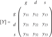
A linear n-port network is completely characterized by n independent excitation variables and n dependent response variables. These variables are the terminal voltages and currents. There are four ways of arranging these independent and dependent variables for a two-port circuit that are particularly useful, especially when considering feedback circuits. They are the impedance parameters (z matrix), admittance parameters (y matrix), hybrid parameters (h matrix), and the inverse hybrid parameters (g matrix). These four sets of parameters are defined as:
(4.1)
![]()
(4.2)
![]()
(4.3)
![]()
(4.4)
![]()
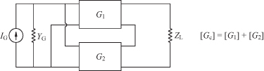
Two networks connected in series (Fig. 4.1) can be combined by simply adding the z parameters of each network together. This configuration is called the series–series connection. In the shunt–shunt configuration shown in Fig. 4.2, the two circuits can be combined by adding their y matrices together. In the series–shunt configuration (Fig. 4.3), the composite matrix for the combination is found by adding the h parameters of each circuit together. Finally, the circuits connected in the shunt–series configuration (Fig. 4.4) can be combined by adding the g parameters of the respective circuits. In each case the independent variables for the particular configuration are the same for each of the individual circuits; thus matrix addition is valid most of the time. The case where the matrix addition is not valid occurs when, for example, in Fig. 4.1 a current going in and out of port 1 of circuit 1 is not equal to the current going in and out of port 1 of circuit 2. These pathological cases will not be of concern here, but further information is found in [1, pp. 188–191] where a description of the Brune test is given.
FIGURE 4.1 Series–series connection.
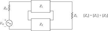
FIGURE 4.2 Shunt–shunt connection.
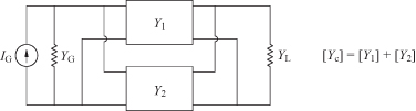
FIGURE 4.3 Series–shunt connection.
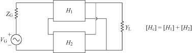
FIGURE 4.4 Shunt–series connection.
Any of the four types of circuit parameters described above can be represented by an equivalent circuit with controlled sources. As an example, the impedance (or z) parameters can be represented as shown in Fig. 4.5. The input port 1 side is represented by a series resistance of value z11 together with a current-controlled voltage source with gain z12 in series. The controlling current is the port 2 current. If the current at port 1 is i1 and the current at port 2 is i2, then the voltage at port 1 is
![]()
FIGURE 4.5 Equivalent circuit for z parameters.
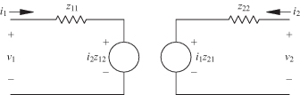
A similar representation is used for the port 2 side.
The individual impedance parameters are found for a given circuit by setting i1 or i2 to 0 and solving for the appropriate z parameter. The z parameters are sometimes termed the open-circuit parameters for this reason. The y parameters are sometimes called the short-circuit parameters because they are found by shorting the appropriate port. The conversion of these parameters is summarized in Appendix D.
4.2 ABCD PARAMETERS
Two-port networks are often cascaded together, and it would be useful to be able to describe each network in such a way that the product of the matrices of each individual network would describe the total composite cascaded network. The ABCD parameters have the property of having the port 1 variables being the independent variables and the port 2 variables being the dependent ones:
This allows the cascade of two networks to be represented as the matrix product of the two circuits expressed in terms of the ABCD parameters. The ABCD parameters can be expressed in terms of the commonly used z parameters:
(4.6)
![]()
(4.7)
![]()
(4.8)
![]()
(4.9)
![]()
where
![]()
In addition, if the circuit is reciprocal so that z12 = z21, then the determinate of the ABCD matrix is unity, namely
(4.10)
![]()
4.3 IMAGE IMPEDANCE
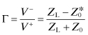
A generator impedance is said to be matched to a load when the generator can deliver the maximum power to the load. This occurs when the generator impedance is the complex conjugate of the load impedance. For a two-port circuit, the generator delivers power to the circuit, which in turn has a certain load impedance attached to the other side (Fig. 4.6). Consequently, maximum power transfer from the generator to the input of the two-port circuit occurs when it has the appropriate load impedance, ZL. The optimum generator impedance depends on both the two-port circuit itself and its load impedance. In addition, the matched load impedance at the output side will depend on the two-port itself as well as the generator impedance on the input side. Both sides are matched simultaneously when the input side is terminated with an impedance equal to its image impedance, ZI1, and the output side is terminated with a load impedance equal to ZI2. The actual values for ZI1 and ZI2 are determined completely by the two-port circuit itself and are independent of the loading on either side of the circuit. Terminating the two-port circuit in this way will guarantee maximum power transfer from the generator into the input side and maximum power transfer from a generator at the output side (if it exists).
FIGURE 4.6 Excitation of a two-port circuit at port 1.
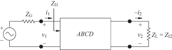
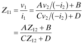
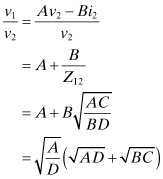
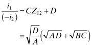
The volt–ampere equations for a two-port circuit are given in terms of their ABCD parameters as
If the input port is terminated by ZI1 = v1/i1, and the output port by ZI2 = v2/(−i2), then both sides will be matched. Taking the ratio of Eqs. (4.11) and (4.12) gives
The voltage and current for the output side in terms of these parameters of the input side are found by inverting Eqs. (4.11) and (4.12):
(4.14)
![]()
(4.15)
![]()
If the output port is excited by v2 as shown in Fig. 4.7, then the matched load impedance is the same as the image impedance:
FIGURE 4.7 Excitation of a two-port circuit at port 2.
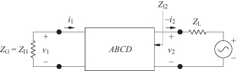
Equations (4.13) and (4.16) can be solved to find the image impedances for both sides of the circuit:
(4.17)
![]()
(4.18)
![]()
When a two-port circuit is terminated on each side by its image impedance, so that ZG = ZI1 and ZL = ZI2, then the circuit is matched on both sides simultaneously. The input impedance is ZI1 if the load impedance is ZI2 and vice versa.
The image impedance can be written in terms of the open-circuit z parameters and the short-circuit y parameters by making the appropriate substitutions for the ABCD parameters (see Appendix D):
(4.19)
![]()
(4.20)
![]()
Therefore, an easy way to remember the values for the image impedances is
(4.21)
![]()
(4.22)
![]()
where zoc1 and zsc1 are the input impedances of the two-port circuit when the output port is an open circuit or a short circuit, respectively.
As an example consider the simple T circuit in Fig. 4.8. The input impedance when the output is an open circuit is
(4.23)
![]()
and the input impedance when the output is a short circuit is
(4.24)
![]()
FIGURE 4.8 Example T circuit.
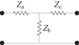
The image impedance for the input port for this circuit is
(4.25)
![]()
and similarly for the output port
(4.26)
![]()
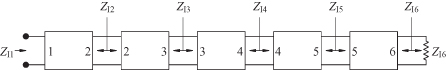
The output side of the two-port circuit can be replaced by another two-port circuit whose input impedance is ZI2. This is possible if ZI2 is the image impedance of the second circuit and the load of the second circuit is equal to its output image impedance, say ZI3. A cascade of two-port circuits where each port is terminated by its image impedance would be matched everywhere (Fig. 4.9). A wave entering from the left side could propagate through the entire chain of two-port circuits without any internal reflections. There, of course, could be some attenuation if the two-port circuits contain lossy elements.
FIGURE 4.9 Chain of matched two-port circuits.
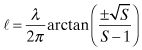
The image propagation constant, γ, for a two-port circuit is defined as
If the network is symmetrical so that ZI1 = ZI2, then eγ = v1/v2. For the general unsymmetrical network, the ratio v1/v2 is found from Eq. (4.11) as
Similarly,
The image propagation constant is obtained from Eq. (4.27):
Also,
When the circuit is reciprocal, AD − BC = 1. Now if Eqs. (4.28) and (4.29) are added together and then subtracted from one another, the image propagation constant can be expressed in terms of hyperbolic functions.
(4.30)
![]()
(4.31)
![]()
If n represents the square root of the image impedance ratio, the ABCD parameters can then be written in terms of n and γ.
(4.32)

(4.33)
![]()
(4.34)
![]()
(4.35)
![]()
(4.36)
![]()
Hence, from the definition of the ABCD matrix, Eq. (4.5), the terminal voltages and currents can be written in terms of n and γ:
(4.37)
![]()
(4.38)
![]()
Division of these two equations gives the input impedance of the two-port circuit when it is terminated by ZL:
(4.39)
![]()
This is simply the transmission line equation for a lumped-parameter network when the output is terminated by ZL = v2/(−i2). A clear distinction should be drawn between the input impedance of the network, Zin, which depends on the value of ZL, and the image impedance ZI2, which depends only on the two-port circuit itself. For a standard transmission line, ZI1 = ZI2 = Z0 where Z0 is the characteristic impedance of the transmission line. Just as for the image impedance, the characteristic impedance does not depend on the terminating impedances, but is a function of the geometrical features of the transmission line itself. When the lumped-parameter circuit is lossless, γ = jβ is pure imaginary and the hyperbolic functions become trigonometric functions:
(4.40)
![]()
where β is real. For a lossless
transmission line of electrical length θ = ω![]() /v,
/v,
where ω is the radian frequency,
![]() is the length of the
transmission line, and v is the velocity of propagation
in the transmission line medium.
is the length of the
transmission line, and v is the velocity of propagation
in the transmission line medium.
4.4 TELEGRAPHER’S EQUATIONS
A transmission line consists of two conductors that are spaced considerably less than a quarter wavelength apart. The transmission line is assumed to support only a transverse electromagnetic (TEM) wave. The transmission line might support higher order modes at higher frequencies, but it is assumed here that only the TEM wave is present. This assumption applies to the vast number of two conductor transmission lines used in practice. A transmission line may take a wide variety of forms: Here it will be represented as a two-wire transmssion line (Fig. 4.10). This line is represented as having a certain series inductance per unit length, L, and a certain shunt capacitance per unit length, C (Fig. 4.11). The inductance for the differential length is thus L dz, and the capacitance is C dz. If the incoming voltage and current wave entering port 1 is V = v1 and I = i1, respectively, then the voltage at port 2 is
![]()
FIGURE 4.10 Two-wire representation of transmission line.
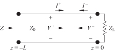
FIGURE 4.11 Circuit model of a differential length of transmission line where (a) is the lossless line and (b) is the lossy line.
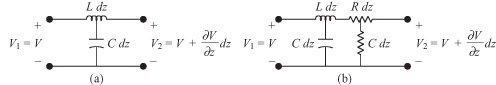
so that the voltage difference between ports 1 and 2 is
(4.42)
![]()
The negative sign for the derivative indicates the voltage is decreasing in going from port 1 to port 2. Similarly, the difference in current from port 1 to port 2 is the current going through the shunt capacitance:
(4.43)
![]()
The telegrapher’s equations are obtained from (4.42) and (4.43):
Differentiation of Eq. (4.44) with respect to z and Eq. (4.45) with respect to t and then combining produces the voltage wave equation:
In similar fashion the current wave equation can be found:
The velocity of the wave is
(4.48)
![]()
The solution for these two wave equations given below in terms of the arbitray functions F1 and F2 can be verified by substitution back into Eqs. (4.46) and (4.47):
(4.49)
![]()
(4.50)
![]()
The most useful function for F1 and F2 is the exponential function exp[j(ωt ± βz)] where β = ω/v. The term, Z0, is the same characteristic impedance used in Eq. (4.41) for the transmission line. For the telegrapher’s equations it is
The units for L and C are given in terms of henries per unit length and farads per unit length. These are to be distinguished from L and C used in lumpded-element circuit theory.
4.5 TRANSMISSION LINE EQUATION
The transmission line equation was determined in Section 4.3
for a cascade of lumped-element matched circuits. It is the input impedance of a
transmission line terminated with a load, ZL,
and it can also be found directly from analysis of a transmission line itself. The
transmission line is characterized by its mechanical length, ![]() , and its characteristic
impedance, Z0. The characteristic impedance
of a transmission line is a function only of the geometry and dielectric constant of
the material between the conductors and is independent of its terminating
impedances. This is similar to the image impedance for lumped-element circuits. The
input impedance of the transmission line depends on
, and its characteristic
impedance, Z0. The characteristic impedance
of a transmission line is a function only of the geometry and dielectric constant of
the material between the conductors and is independent of its terminating
impedances. This is similar to the image impedance for lumped-element circuits. The
input impedance of the transmission line depends on ![]() , Z0, and ZL. When
terminated with a nonmatching impedance, a standing wave is set up in the
transmission line where the forward- and backward-going voltages and currents are as
indicated in Fig. 4.10. At the
load,
, Z0, and ZL. When
terminated with a nonmatching impedance, a standing wave is set up in the
transmission line where the forward- and backward-going voltages and currents are as
indicated in Fig. 4.10. At the
load,
(4.53)
![]()
Since the forward current wave is I+ = V+/Z0 and the reverse current wave is I− = V−/Z0, the current at the load is
(4.54)
![]()
Replacing VL above with Eq. (4.52), the voltage reflection coefficient can be determined:
(4.55)
![]()
If the transmssion line is lossy, the reflection coefficent is actually
(4.56)
The phase velocity of the wave is a measure of how fast a given phase moves down a transmission line. This is illustrated in Fig. 4.12 where ejωt time dependence is assumed. If time progresses from t1 to t2, then in order for ej(ωt−βz) to have the same phase at each of these two times, the wave must progress in the forward direction from z1 to z2. Consequently,
![]()
FIGURE 4.12 Forward directed propagating wave.
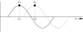
giving the phase velocity
(4.57)
![]()
This is to be distinguished from the group velocity,
![]()
which is a measure of velocity of energy flow. For low loss media, vgv = c2/ε where c is the velocity of light in a vacuum. The negative-going wave, of course, has a phase velocity of −ω/β.
This traveling wave corresponds to the solution of the lossless telegrapher’s equations. The total voltage at any position, z, along the transmission line would be the sum of the forward- and backward-going waves:
The total current at any point z is by Kirchhoff’s law the difference of the two currents:
At the input to the line (or left side) where z = −![]() , the ratio of Eqs. (4.58) and (4.59) gives the input impedance:
, the ratio of Eqs. (4.58) and (4.59) gives the input impedance:
(4.61)
![]()
At the position z = −![]()
If the propagation constant is the complex quantity γ = α + jβ, then
(4.63)
![]()
A few special cases illustrates some basic features of the transmission
line equation. If z = 0, Zin(0) = ZL no matter
what Z0 is. If ZL = Z0, then Zin(z) = Z0 no matter what z
is. For a quarter wavelength line, ![]() .
The input impedance for any length of line can be readily calculated from Eq. (4.62) or by using the Smith
chart.
.
The input impedance for any length of line can be readily calculated from Eq. (4.62) or by using the Smith
chart.
4.6 SMITH CHART
The Smith chart, as shown in Fig. 4.13, is merely a plot of the transmission line equation
on a set of polar coordinates. The reflection coefficient is really an alternate way
of expressing the input impedance relative to some standard value (Z0), which is typically 50 ![]() . The
reflection coefficient, Γ, has a magnitude between 0 and 1 and a phase angle between
0 ° and 360 °. The equations describing the radii and centers of the circles of the
coordinates of the Smith chart are found by solving the normalized version of Eq. (4.60):
. The
reflection coefficient, Γ, has a magnitude between 0 and 1 and a phase angle between
0 ° and 360 °. The equations describing the radii and centers of the circles of the
coordinates of the Smith chart are found by solving the normalized version of Eq. (4.60):
FIGURE 4.13 Smith chart.
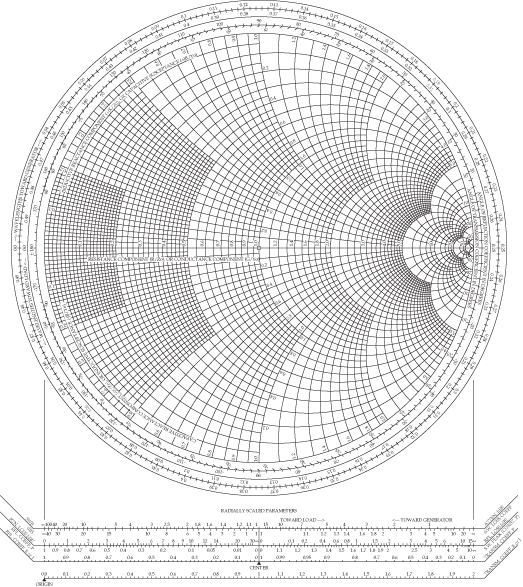
Solution of the real part of Eq. (4.64) gives the center of the resistance circles as (r/(1 + r), 0) with a radius of 1/(1 + r). Solution of the imaginary part gives the center of the reactance circles as (1, 1/x) with a radius of 1/x [2, pp. 121–129].
The Smith chart can be used as a computational tool, and it often gives insight where straight equation solving will not. It is also a convenient plotting tool of measured or calculated data, since any passive impedance will fall within its boundaries.
4.7 TRANSMISSION LINE STUB TRANSFORMER
In Chapter 3 a variety of lumped-element impedance transformers were described. Impedance transformation can also be achieved using a simple transmission line circuit with a shunt or series stub. The shunt stub design is the most practical for the most common types of transmission lines. When the transmission line and stub lengths are a small fraction of a wavelength, the circuit can be practical for the upper RF range. Impedance matching can be done using either short-circuit or open-circuit stubs. Impedance matching can be done using shunt or series stubs. Finally, it can be done with one, two, or three stubs as described by Collin [3].
4.7.1 Matching a Real Load Impedance
Consider the shunt stub circuit shown in Fig. 4.14. The load admittance, YL, is to be matched to the generator side whose admittance is YG = Y0. A distance, d, is determined so that the admittance looking toward the load just to the right side of the stub is
(4.65)
![]()
FIGURE 4.14 Open- or short-circuit stub-matching circuit with YL complex. When YL is real, d2 = 0 and ΓL = ± |ΓL|.
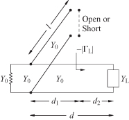
When YL is real as is assumed
here, then d2 = 0 and ΓL = ± |ΓL| in Fig. 4.14. At the intersection of the main line and the shunt
stub, the shunt stub is designed to produce a shunt admittance of −jB, which cancels the susceptance of ![]() in leaving
in leaving
(4.66)
![]()
Because of the periodicity of the tangent function, there are many
solutions for d and shunt stub length ![]() . The admittance repeats
for each added half wavelength, nλ/2. Usually it is wise
to choose the smallest values for d and
. The admittance repeats
for each added half wavelength, nλ/2. Usually it is wise
to choose the smallest values for d and ![]() in order to minimize
frequency sensitivity. The end of the stub may be either a short or an open circuit
to ground. When the stub length is shorter than a quarter wavelength, then
in order to minimize
frequency sensitivity. The end of the stub may be either a short or an open circuit
to ground. When the stub length is shorter than a quarter wavelength, then
(4.67)
![]()
Knowing the sign of the required susceptance determines whether to use
an open- or a short-circuited stub to achieve the minimum distance, ![]() .
.
The characteristic admittance used in each of the transmission lines can
be any realizable value, but for simplicity the value is chosen to be the system
characteristic admittance, Y0. Then the only
two design parameters that need to be found are d and
![]() .
.
The load admittance is assumed to be real, so that YL = GL. This restriction will be removed later. At a distance d from the load,
(4.68)
![]()
(4.69)
![]()
where θ = βd. The real and imaginary parts of this equation are
(4.70)
![]()
(4.71)
![]()
which are, respectively,
Substitution of Eq. (4.73) into Eq. (4.72) gives
A useful alternative form makes use of the trigonometric double-angle formula
(4.75)
![]()
so that
The ambiguity in the sign for the ![]() in Eq. (4.74) is
used to determine the stub length
in Eq. (4.74) is
used to determine the stub length ![]() . The + sign is chosen
when 0 < βd1 < π/2 or when 0 < d1 < λ/4. The − sign is
chosen when λ/4 < d1 < λ/2. From Eqs. (4.73) and (4.74)
. The + sign is chosen
when 0 < βd1 < π/2 or when 0 < d1 < λ/4. The − sign is
chosen when λ/4 < d1 < λ/2. From Eqs. (4.73) and (4.74)
The transmission line equation gives the input admittance for a short-circuit stub as
(4.79)
![]()
so that from Eq. (4.78)
or
The design is complete since the characteristic admittance and length of each line section have been found. The design of the open-circuit stub is similar and will be given after considering matching to a complex load.
4.7.2 Matching a Complex Load Impedance
The voltage across the transmission line varies sinusoidally as a function of the position along the line. At a certain point, the voltage will reach a minimum as inferred by Eq. (4.58):
(4.82)
![]()
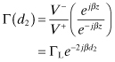
Since Γ = |Γ| exp(jψ), then at a certain point, d2, Γ will be negative and real (Fig. 4.14):
(4.83)
![]()
Here the admittance is maximum and real:
(4.84)
![]()
The variable, S, is the voltage standing-wave ratio, which is a scalar ratio of the maximum to minimum voltage on the transmission line. Moving from the load admittance, YL, a distance d2 will give an admittance looking toward the load a real value of Y0S for the “load” at position d2. The equations for the real load admittance can now be used where GL = Y0S. From Eqs. (4.76), (4.77), and (4.81)
(4.86)
![]()
Choose the ![]() when 0
< d1 < λ/4 and
when 0
< d1 < λ/4 and ![]() when λ/4 < d1
< λ/2. The total distance from the complex load,
YL, to the stub is
when λ/4 < d1
< λ/2. The total distance from the complex load,
YL, to the stub is
(4.89)
![]()
where d1 is the same solution for d in Section 4.7.1 (Eq. 4.76).
The above designs have been based on the use of a short-circuit stub. However, the open circuit is often easier to implement. If the susceptance from the load at d turns out to be negative, the open-circuit stub will provide the shortest line length to get the positive susceptance needed for cancellation. The input admittance for an open-circuit stub is jY0 tan ϕ. Then by analogy with Eqs. (4.80) and (4.81),
(4.90)
![]()
(4.91)
![]()
or for a complex load
(4.92)
![]()
As an example, design a matching circuit for a load impedance of ZL = 30 + j40 ![]() with
Z0 = 50
with
Z0 = 50 ![]() using a
short-circuit stub. The reflection coefficient at the load is
using a
short-circuit stub. The reflection coefficient at the load is
![]()
The magnitude of ΓL is 0.5 and the angle ψ is π/2. Since,
The sign change in Eq. (4.93) is a result of placing the origin at the load and moving in the −z direction toward the generator a distance of d2. The minus sign is used to ensure positive line lengths for d2. Solving Eqs. (4.94) and (4.95) for d2 gives
(4.96)
![]()
In the present example, ψ = π/2 so that d2 =
0.375λ. From Eq. (4.85) the standing-wave ratio, S = 3, from Eq. (4.87)
d1 = 0.0833 λ so
that d = d1 +
d2 = 0.4583 λ, and from Eq. (4.88)
![]() = 0.205 λ.
= 0.205 λ.
4.8 COMMONLY USED TRANSMISSION LINES
Because TEM transmission lines have neither an elecrtric nor magnetic field component in the direction of propagation, the characteristic impedance can be found from Eq. (4.51) and electrostatics. Since the velocity of propagation in the given media is presumably known, all that is necessary is to calculate the electrostatic capacitance between the conductors. When the geometry is particularly nasty and the solution is needed quickly, the field mapping approach described in Section 2.2.2 can be used.
4.8.1 Two-Wire Transmission Line
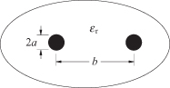
The two-wire transmission line commonly used, for example, between a TV antenna and the receiver, consists of two round conductors each with a radius of a and separated by a distance b (Fig. 4.15). The dielectric surrounding the wires has a dielectric constant of ε. The field theory analysis, such as that given in [2], shows that the characteristic impedance of the two-wire line is
(4.97)
![]()
where
(4.98)
![]()
FIGURE 4.15 Two-wire transmission line.
While the field analysis for a given structure may bring some challenges, the good news is that once Z0 is known, the rest of the problem can be solved by circuit theory. Losses in the two-wire transmission line stem from the lossy dielectric between the conductors and the resistive losses experienced by the current as it flows along the conductor. Since a voltage wave is attenuated as it goes down a line by exp(−αz), the power loss is proportional to exp(−2αz) where
The dielectric and conductor losses are
(4.100)
![]()
(4.101)
![]()
where σd and σc are the conductivities of the dielectric and conductor, respectively. The two-wire line is inexpensive and widely used in ultrahigh frequency (UHF) applications.
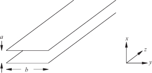
4.8.2 Parallel Strip Transmission Line
The parallel strip transmission line consists of two separate conductors of width b and separated by a distance a (Fig. 4.16). This is a rectangular waveguide without the side walls. It is fundamentally distinct from the rectangular waveguide, which is not a TEM transmission line. The Maxwell equations for a plane wave for this system are the exact analog to the telegrapher’s equations:
FIGURE 4.16 Parallel strip transmission line.
The voltage between the strips is the integral of the electric field:
The magnetic field in the y direction will produce a current in the conductor that will travel in the z direction according to Ampère’s law:
Substitution of Eqs. (4.104) and (4.105) into Eq. (4.44) gives
(4.106)
![]()
Comparison of this with Eq. (4.102) indicates that
(4.107)
![]()
A similar substitution of Eqs. (4.104) and (4.105) into Eq. (4.45) and comparison with Eq. (4.103) indicates that
(4.108)
![]()
so that the characteristic impedance for the parallel strip guide is
While this solution illustrates the major feactures of the parallel strip transmission line, the neglect of the fringing fields makes this expression in practice useless. A more uselful expression was developed for the parallel strip line [4], which was later used to determine the characteristic impedance for microstrip by the method of images (Fig. 4.17). Conformal transformations of the structure were made that included an approximation of the fringing fields. As a result two formulas were developed, one for wide and the other for narrow strips. The analysis formulas follow:
(4.110)
![]()
(4.111)
![]()
FIGURE 4.17 Relationship between parallel strip line and microstrip by method of images.
for b/a < 0.56 and
for b/a > 0.56.
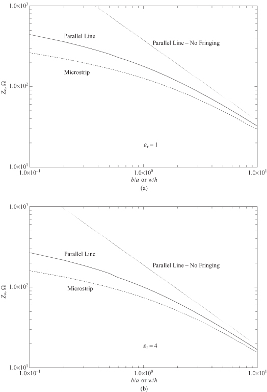
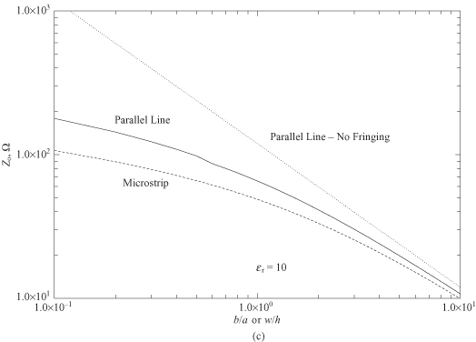
Equation (4.112) is Eq. (48) in [4] and Eq. (4.113) is Eq. (31) in [4] except that here b/a represents 2a/2b in [4]. The method of images then can be invoked to find the characteristic impedance of the microstrip. This is described more fully in Section 4.8.4. A comparison of Eq. (4.109) with no fringing capacitance, and the formula that includes fringing capacitance, Eqs. (4.112) and (4.113), as well as the microstrip is shown in Fig. 4.17 (a, b, and c) for εr = 1, 4, and 10, respectively. A parallel strip line with a given b/a ratio will give a certain value for Z0. A microstrip line with w/h = b/(a/2) would give a characteristic impedance of Z0/2. The equations used for the microstrip calculation are those in Section 4.8.4, so the factor of 2 is close, but not exact.
4.8.3 Coaxial Transmission Line
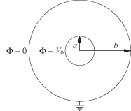
A coaxial transmission line comes in the form of rigid, semirigid, and flexible forms. The end view of a coaxial line, which is shown in Fig. 4.18, consists of an inner conductor and the outer conductor, which is normally grounded. The electric field points from the center to the outer conductor, and the longitudinal current on the center conductor produces a magnetic field concentric to the inner conductor. The potential between the two conductors is a solution of the transverse form of Laplace’s equation in cylindrical coordinates where there is no potential difference in the longitudinal z direction. The notation for the divergence and curl operators follows that given in [5]:
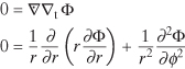
FIGURE 4.18 Characteristic impedance for parallel strip line (with and without fringing) and microstrip for (a) εr = 1, (b) εr = 4, and (c) εr = 10. b/a corresponds to parallel strip line and w/h corresponds to microstrip.
Because there is no potential variation in the z direction, the z derivative of Φ is zero. Because of symmetry, there is no variation of Φ in the ϕ direction either. Thus, Eq. (4.114) simplifies to an ordinary second-order differential equation subject to the boundary conditions that Φ = 0 on the outer conductor and Φ = V0 on the inner conductor:
Integration of Eq. (4.115) twice gives
(4.116)
![]()
which upon applying the boundary conditions gives the potential anywhere between the two conductors:
(4.117)
![]()
The electric field is easily obtained by differentiation.
(4.118)
![]()
The magnetic field is then
(4.119)
FIGURE 4.19 Coaxial transmission line.
The outward normal unit vector of the center conductor, ![]() , is shown in Fig. 4.20. The surface current on the
center conductor is determined by the boundary condition for the tangential magnetic
field:
, is shown in Fig. 4.20. The surface current on the
center conductor is determined by the boundary condition for the tangential magnetic
field:
(4.120)
![]()
FIGURE 4.20 Continuity of magnetic field along center conductor.

The later result occurs because the magnetic field is zero inside the conductor. The total current flowing in the center conductor is
(4.121)
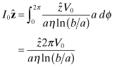
so that
(4.122)
![]()
Coaxial Dielectric Loss
The differential form of Ampère’s law relates the magnetic field to both the conduction current and the displacement current. In the absence of a conductor
By taking the curl of Eq. (4.124), the Helmholtz wave equation for H can be found. A solution of the wave equation would give the propagation constant, γ:
where εr is the relative dielectric constant and k0 is the propagation constant in free space. A lossy dielectric is typically represented as the sum of the lossless (real) and lossy (imaginary) parts:
The revised propagation constant is found by substituting this into Eq.
(4.125). The result can be
simplified by taking the first two terms of the Taylor series expansion since ![]() .
.
(4.127)
![]()
so that
(4.128)
![]()
(4.129)
![]()
The power loss is proportional to exp(−2αz).
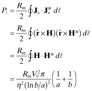
Coaxial Conductor Loss
The power loss per unit length, P![]() , is obtained by taking
the derivative of the power at a given point along a transmission line:
, is obtained by taking
the derivative of the power at a given point along a transmission line:
(4.130)
![]()
For a low loss conductor where the dielectric losses are negligible, Eq. (4.123) becomes with the help of Ohm’s law,
(4.132)
![]()
where σ is the metal conductivity. This would be the same equation as Eq. (4.124) if
(4.133)
![]()
With this substitution the wave impedance becomes the metal surface impedance:
At the surface there will be a longitudinal electric field of ZmJs
directed in the ![]() direction. Thus, in
a lossy line, the fields will no longer be strictly TEM. This longitudinal electric
field produces energy flow into the conductor proportional to
direction. Thus, in
a lossy line, the fields will no longer be strictly TEM. This longitudinal electric
field produces energy flow into the conductor proportional to ![]() . This energy is dissipated in the
center and outer conductors. The power loss per unit length is found in the
following way:
. This energy is dissipated in the
center and outer conductors. The power loss per unit length is found in the
following way:
(4.135)
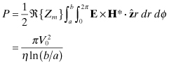
The power, P, transmitted down the line is found by the Poynting theorem:
(4.136)
The attenuation constant associated with conductor loss is found from Eq. (4.131):
(4.137)
![]()
while the dielectric loss found earlier is
(4.138)
![]()
The total loss is found from Eq. (4.99).
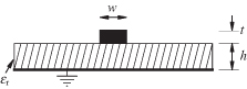
4.8.4 Microstrip Transmission Line
Microstrip has been a popular form of transmission line for RF and microwave frequencies for some time. The microstrip line shown in Fig. 4.21 consists of a conductor strip of width w on a dielectric of thickness h above a ground plane. Part of the electric field between the strip and the ground plane is in the dielectric and part in the air. The field is more concentrated in the dielectric than in the air. Consequently, the effective dielectric constant, εeff, is somewhere between εr and 1, but closer to εr than 1. A variety of methods have been used to find εeff. However, rather than provide a proof, a simple empirically based procedure for synthesizing a microstrip line will be given. A microstrip line is not strictly a TEM type of transmission line and does have some frequency dispersion. Unless microstrip is being used in a wide bandwidth application, the TEM approximation should be adequate. Determining the characteristic impedance could be done by using the parallel strip line described earlier and the method of images. The microstrip ground plane reflects the image of the narrow strip so that it would appear to be two strips with dielectric between the strips. This is exactly what was done in [6]. However, since the height of the microstrip line is half the height of the parallel strips, the electric field between the two conductors in the microstrip will be twice as strong, the capacitance would be twice as large, so Z0 is half as large as the eqivalent paralle strip line. The synthesis problem occurs when the desired characteristic impedance, Z0, and the dielectric constant of the substrate, εr, are known and the geometrical quantity w/h is to be found. The synthesis equations, given by [6] are simple, and give an approximate solution to the microstrip problem.
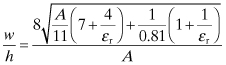
FIGURE 4.21 Microstrip transmission line.
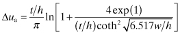
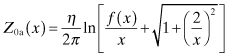
The analysis equations given below by [7] are more accurate than the synthesis equations. The value given by Eqs. (4.139) and (4.140) provides an ititial value for w/h that can be used in an iterative procedure to successfully solve the synthesis problem. This process depends on knowing εr, and the conductor thickness, t. The solution results in the effective dielectric constant, εeff, needed to determine electrical line lengths and Z0. The procedure for the analysis procedure follows:
(4.141)
(4.142)
![]()
(4.143)
![]()
(4.144)
![]()
(4.145)
(4.146)
![]()
(4.147)
![]()
(4.148)
(4.149)
![]()
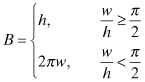
From the given value of t and trial solutions of w/h, Eqs. (4.141) to (4.144) give unique values for ua and ur. In Eqs. (4.145) through (4.148), x is replaced by ua or ur as required by the calculation for Z0 and εeff in Eqs (4.150) and (4.151):
Since w/h increases when Z0 decreases and vice versa, one very simple and effective method for finding the new approximation for w/h is done by using the following ratio:
(4.152)
![]()
For example, if w/h for trial i is too small, the resulting Z0 will increase the value for w/h in trial i + 1. This procedure has been coded in the program MICSTP, which will converge to a value for Z0 with acceptable error within five iterations when given an initial value from Eq. (4.139).
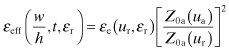
The effect of dielectric and conductor loss is summarized here [8–10]:
(4.153)
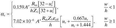
(4.154)
![]()
(4.155)
The value for the loss caused by the dielectric is
(4.156)
![]()
where the wave number in vacuum is k0. The definition for Rm, ![]() , and
, and ![]() were given previously as the real
part of Eq. (4.134) and the complex
parts of Eq. (4.126),
respectively.
were given previously as the real
part of Eq. (4.134) and the complex
parts of Eq. (4.126),
respectively.
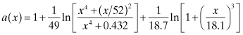
While actual microstrip transmission lines are somewhat dispersive, the above analysis presumes that the effective dielectric constant is independent of frequency. Design of broadband circuits will sometimes require knowledge of how εeff varies with frequency. An accurate formula suitable for computer-aided design is given by [11]. In these expressions, frequency f is in gigahertz, h, and w are in centimeters:
(4.157)
![]()
where
(4.158)
![]()
(4.159)
![]()
(4.160)
![]()
(4.161)
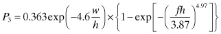
(4.162)
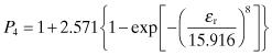
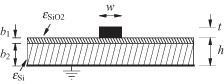
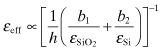
These equations for Z0 and εeff are widely accepted as the most accurate available for the quasi-TEM microstrip transmission line. Typical silicon integrated circuit transmission lines have a more complicated structure. The “dielectric” under the metal line typically consists of a thin layer of SiO2 approximately 0.5 to 1 µm thick and a Si substrate that could be approximately 200 µm thick (Fig. 4.22). This results in three distinct propagation modes: (1) the dielectric quasi-TEM mode, (2) the skin effect mode, and (3) the slow wave mode [12]. The analysis of these modes is an approximation based on the transverse resonance technique for parallel plate waveguide. The SiO2 layer is low loss and thin. The Si layer is thick and has a conductivity, σ, dependent on its doping.
FIGURE 4.22 Microstrip transmission line in Si-integrated circuits.
The dielectric quasi-TEM mode occurs when ω/σ is large so that the Si substrate layer is low loss and acts as a dielectric. If the signal wavelength is much greater than the double-layer thickness, h, then propagation will be almost TEM. For this case the dielectric constant is
(4.163)
The skin effect mode occurs when ωσ is large
so that the Si substrate acts as a lossy conductor wall. The skin depth, ![]() , is large enough to allow signficant
penetration of the fields into the Si. Propagation in this mode is highly
dispersive. In this case
, is large enough to allow signficant
penetration of the fields into the Si. Propagation in this mode is highly
dispersive. In this case
(4.165)
![]()
The slow wave mode occurs when ω is not too high and σ is moderate. The dielectric constant is similar to that found for the skin effect mode in Eq. (4.164), but the permeability is back to μ0. The effective dielectric constant is multipled by the h/b1 ratio, thereby producing slow wave propagation. With the right conductivity, this slow wave mode can extend into the low gigahertz range. It normally pays to stay out of this range in RF circuits. When ωσ is sufficiently small, the field can penetrate to the ground plane.
In multiple layer structures, it is possible to have two metals separted by Si where one metal would act as the ground. Depending on the metal width, it could be used as either microstrip with possibly an over layer or parallel plate line. The t/h ratio for integrated circuit lines will typically be much larger than that used in printed circuit boards. A large metal thickness will then decrease the required metal width for a given Z0.
There are a variety of other transmission line geometries that could be studied, but these examples should provide information on the most widely used forms. There are cases where one line is located close enough to a neighboring line that there is some electromagnetic coupling between them. There are cases where interactions between discontinuities or nearby structures would preclude an analytic solution. In such cases, solutions can be found from 2.5- and 3-dimensional numerical Maxwell equation solvers.
4.9 SCATTERING PARAMETERS
This chapter began with a discussion of five ways of describing a two-port circuit in terms of its terminal voltages and currents. In principle any one of these is sufficent. One of these, the h parameters, was popularized during the early days of the bipolar transistor since they could be directly measured for a transistor. For a similar reason, scattering parameters, or S parameters, have been found convenient by RF and microwave engineers because circuits can be directly measured in terms of them at these frequencies. Scattering parameters represent reflection and transmission coefficients of waves, a quantity that can be measured directly at RF and microwave frequencies. However, these wave quantities can be directly related to the terminal voltages and currents, so that there is a relationship between the scattering paramters and the z, y, h, g, and ABCD parameters.
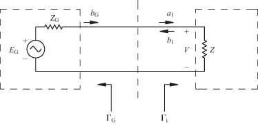
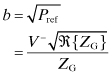
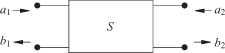
Consider a one-port circuit excited with a voltage source EG with an internal generator impedance, ZG, as shown in Fig. 4.23. Quantity a represents the wave entering into the port. Quantity b represents the wave leaving the port. Both of these quantities are complex and can be related to the terminal voltage and current. The generator and the load are characterized by a reflection coefficient, ΓG and Γi, respectively. The wave bG from the generator undergoes multiple reflections until finally the reflected wave from the load, b1, is obtained:
(4.166)
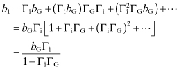
FIGURE 4.23 Wave reflections from unmatched generator source.
This last expression is the sum of a geometric series. Since Γi = b1/a1, an expression for the wave entering into the load can be found:
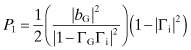
The power actually delivered to the load is then
(4.168)
![]()
From the definition of Γi and Eq. (4.167), the delivered power can be found:
(4.169)
and when matched so that ![]() :
:
(4.170)
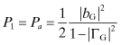
The latter is the available power from the source. Similar expressions could be found for an n-port circuit.
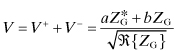
The wave values will be related to the terminal voltages and currents. With reference to Fig. 4.23, Ohm’s law gives
(4.171)
![]()
A forward-going voltage wave, V+, can be related to the forward-going current by
(4.172)
![]()
The reason for this is that if ![]() , V = V+, because V− = 0.
Similarly,
, V = V+, because V− = 0.
Similarly,
(4.173)
![]()
The forward-going voltage and current can be expressed by means of Ohm’s law as follows:
(4.174)
(4.175)
![]()
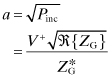
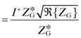
These voltages and currents represent root mean square (rms) values, so the incident power is
(4.176)
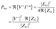
The incident power, Pinc, is
proportional to |a|2 and the reflected power,
Pref, to |b|2. Taking the square root of a number to get a complex
quantity is strictly speaking not possible mathematically unless a choice is made
regarding the phase angle of the complex quantity. This choice is related to
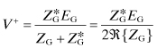
choosing ![]() and V+ for a and ZG and V− for b:
and V+ for a and ZG and V− for b:
(4.177)
and for b,
(4.179)
From Eqs. (4.177) through (4.180) the forward- and reverse-going voltages and currents can be found in terms of the waves a and b. The total voltage and total current are then found.
These are now in the form of two equations where a and b can be solved in terms of V and I. Multiplying Eq. (4.182) by ZG and adding to Eq. (4.181) gives
![]()
which can be solved for a. In a similar fashion b is found:
Ordinarily, the generator impedance is equal to the characteristic impedance of a transmission line to which it is connected. The common way then to write Eqs. (4.183) and (4.184) is in terms of Z0, which is assumed lossless.
The ratio of Eqs. (4.186) and (4.185) is
![]()
where Γ is the reflection coefficient of the wave. The transmission coefficient is defined as the voltage across the load V due to the incident voltage V+:
(4.187)
![]()
This is to be contrasted with the conservation of power represented by |T|2 + |Γ|2 = 1.
For the two-port circuit shown in Fig. 4.24 there are two sets of ingoing and outgoing waves. These four quantities are related together by the scattering matrix.
(4.188)
![]()
FIGURE 4.24 Two-port circuit described with scattering parameters.
The individual S parameters are found by setting one of the independent variables to zero:
![]()
![]()
![]()
![]()
Thus, S11 is the reflection coefficient at port 1 when port 2 is terminated with a matched load. The value, S12, is the reverse transmission coefficient when port 1 is terminated with a matched load. Similarly, S21 is the forward transmission coefficient, and S22 is the port 2 reflection coefficient when port 1 is matched.
The formulas for converting between the scattering parameters and the volt–ampere relations given in Section 4.1 are given in Appendix D. In each of these formulas there is a Z0 because a reflection or transmission coefficient is always relative to a reference impedance, which in this case is Z0. This is further corroborated by Eqs. (4.185) and (4.186) where the wave values are related to a voltage, current, and Z0.
4.10 INDEFINITE ADMITTANCE MATRIX
Typically, a certain node in a circuit is designated as being the ground node. Similarly, in an n-port network, at least one of the terminals is considered to be the ground node. In an n-port circuit in which none of the terminals is considered the reference node, it can be described by the indefinite admittance matrix. This can be used, for example, when converting the y parameters of a common emitter transistor to the y parameters of a common base transistor. The indefinite admittance matrix has the property that the sum of the rows = 0 and the sum of the columns = 0. Thus, the indefinite admittance matrix can be easily obtained from the usual definite y matrix, which has been defined with at least one terminal connected to ground.
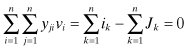
The derivation of this property is based on considering the currents in the indefinite circuit of Fig. 4.25. Let Jk represent the current going into terminal k when all terminals are connected to ground. This current, Jk, is therefore a result of indepenedent current sources inside the n port or currents resulting from initial conditions. The currents going into each terminal are
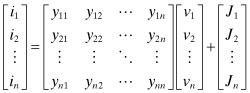
FIGURE 4.25 An n-port indefinite circuit.
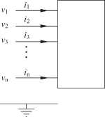
The sum of all the equations represented by Eq. (4.189) gives the total current going into a node, which by Kirchhoff’s law must be zero:
All the terminal voltages except the jth are set to 0 by connecting them to the external ground. Then since vk ≠ 0, the only nonzero term on the left-hand side of Eq. (4.190) would be
(4.191)

Thus, the sum of the columns of the indefinite admittance matrix is 0.
The sum of the rows can also be shown to be 0. If the same voltage v0 is added to each of the terminal voltages, the terminal currents would remain unchanged:
(4.192)
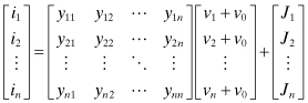
Comparison of this with Eq. (4.189) shows that
(4.193)
Thus, the sum of the rows is 0. A variety of other important properties of the indefinite admittance matrix are described in [1, Chapter 2] to which reference should be made for further details.
One of the useful properties of this concept is illustrated by the problem of converting common source hybrid parameters of an FET to common gate hybrid parameters. This might be useful in designing a common gate oscillator with a transistor characterized as a common source device. The first step in the process is to convert the hybrid parameters to the equivalent definite admittance matrix (which contains 2 rows and 2 columns) by using the formulas in Appendix D. The definite admittance matrix, which has a defined ground, can be changed to the corresponding 3 × 3 indefinite admittance matrix by adding a column and row such that ∑ rows = 0 and the ∑ columns = 0. If the y11 corresponds to the gate and y22 corresponds to the drain, then y33 would correspond to the source.
(4.194)
The common gate parameters are found by forcing the gate voltage to be 0. Consequently, the first column may be removed since it is multiplied by the zero gate voltage anyway. At this point the first row represents a redundant equation and can be removed. Row 1 and column 1 have been deleted and a new common gate definite admittance matrix is formed. This can then be converted to the equivalent common gate hybrid matrix.
4.11 INDEFINITE SCATTERING MATRIX
A similar property can be determined for the scattering matrix. The indefinite scattering matrix has the property that the sum of the rows = 1 and the sum of the colmuns = 1. For the first property, the three-port shown in Fig. 4.26 is excited at all three terminals by the same voltage value. The output wave is
FIGURE 4.26 Indefinite scattering parameter circuit.
Under this excitation, all the input waves, aj, have the same amplitude, so Eq. (4.195) becomes
Since from Eqs. (4.178)
and (4.180)
![]() and
and ![]() , Eq. (4.196) can
be written in terms of the incident and reflected currents:
, Eq. (4.196) can
be written in terms of the incident and reflected currents:
(4.197)
![]()
When all the terminal voltages are set equal, then all the terminal
currents must be zero, since there can be no voltage difference between any two
ports. Thus, ![]() , which means that
, which means that
(4.198)
![]()
proving the sum of the rows = 1.
To show that the sum of the columns = 1, only port 1 is excited with a voltage source. Thus, a1 ≠ 0 and a2 = a3 = 0. By Kirchhoff’s currnet law the sum of the currents into the three terminal circuit is zero:
(4.199)
![]()
(4.200)
![]()
Now since ![]() because of
a2, a3
because of
a2, a3
(4.201)
![]()
In addition
(4.202)

so that
(4.203)
![]()
which shows that the sum of the columns for the indefinite scattering matrix is 1. See the example in Appendix E for converting common source to common gate S parameters.
4.12 CONCLUSIONS
This chpater began with concepts essential for two-port circuit design. The ABCD transmission parameters were used to descirbe a lumped-element analog to the transmission line circuit that pervades all of RF circuit design practice. Various types of transmission lines were described in this chapter: two-wire line, parallel strip line, coaxial line, and microstrip. There are other widely used transmission line structures that are used such as slotline, coplanar line, and assorted types of coupled lines. Finally, scattering parameters were described and used in an indefinite matrix approach similar to that used in lumped-circuit analysis.
PROBLEMS
4.1. Determine the image impedance for the two-port circuit shown in Fig. 4.27, which is terminated by a 5-Ω resistor on each end.
FIGURE 4.27 Image impedance for Problem 4.1.
4.2. If the load side of the circuit in Fig. 4.28 is terminated with its matching
impedance, what is the impedance that will match the input side? In this circuit the
reactance X = ωL = 2 ![]() ,
, ![]() , and
, and ![]() .
.
FIGURE 4.28 Circuit to be matched in Problem 4.2.
4.3. A reciprocal circuit is described in terms of the ABCD parameters, where A = 2, B = 7, and C = 3.
a. What is the value for D?
b. What is the value for the image propagation constant?
c. What is the value for ZI1 and ZI2?
d. If the output were connected
to an impedance ![]() , what would be
the input impedance?
, what would be
the input impedance?
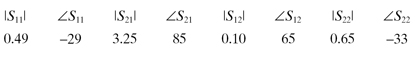
4.4. Convert the following scattering parameters (related to 50
![]() )
to ABCD parameters:
)
to ABCD parameters:
4.5. Given the S parameters, derive the z parameters as given in Table D.1 in Appendix D.
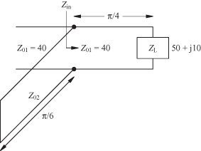
4.6. Two transmission lines are cascaded together as shown in Fig. 4.29. What is the input impedance at the left-hand side of the line?
FIGURE 4.29 Transmission line circuit for Problem 4.6.
4.7. The transmission line circuit of length ![]() and characteristic
impedance Z0 is terminated by a resistance
RL. Determine the Q for this circuit at the first appropriate nonzero frequency.
and characteristic
impedance Z0 is terminated by a resistance
RL. Determine the Q for this circuit at the first appropriate nonzero frequency.
4.8. The impedance of a circuit is given by
![]()
where ![]() = πc/ω0 and c is the velocity of light in a vacuum. What is the Q of this circuit in terms of ω0?
What is the Q of this circuit if
= πc/ω0 and c is the velocity of light in a vacuum. What is the Q of this circuit in terms of ω0?
What is the Q of this circuit if ![]() = 2πc/ω0?
= 2πc/ω0?
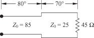
4.9. In the shunt transmission line circuit in Fig. 4.30, determine the value for Z02 that would produce a real value for Zin. What is the value for Zin?
FIGURE 4.30 Shunt transmission line circuit for Problem 4.9.
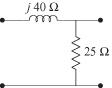
4.10. Determine the S11 scattering parameter for the circuit in Fig. 4.31. Express your answer in the form of a real and imaginary part.
FIGURE 4.31 Circuit for Problem 4.10.
4.11. In the four parts below, design the transmission line when
Z0 = 40 ![]() and
εr = 2.4.
and
εr = 2.4.
a. Determine the wire spacing of a two-wire transmission line that uses wires with a diameter of 80.1 mils (AWG#12) and that are surrounded with a dielectric layer.
b. Design a parallel plate transmission line using a double-sided copper-clad printed circuit board of thickness 0.25 in.
c. Determine the center conductor diameter of a dielectric-filled coaxial line where a standard outer diameter of 0.502 in. is used.
d. Design a microstrip line using a 1-oz copper-clad dielectric board that is 25 mils thick. The 1-oz specification refers to the thickness of the copper, where 1 oz ≈ 1.4 mils. Find the conductor width and effective dielectric constant.
REFERENCES
1. W.-K. Chen, Active Network and Feedback Amplifier Theory, New York: McGraw-Hill, 1980.
2. S. R. Seshadri, Fundamentals of Transmission Lines and Electromagnetic Fields, Reading MA: Addison Wesley, pp. 335–350, 1971.
3. R. E. Collin, Foundations for Microwave Engineering, 2nd ed., New York: McGraw-Hill, 1992.
4. H. A. Wheeler, “Transmission-Line Properties of Parallel Strips Separated by a Dielectric Sheet,” IEEE Trans. Microwave Theory Tech., MTT-13, pp. 172–185, Mar. 1965.
5. C. T. Tai, Generalized Vector and Dyadic Analysis, Piscataway, NJ: IEEE Press, 1997.
6. H. A. Wheeler, “Transmission-Line Properties of a Strip on a Dielectric Sheet on a Plane,” IEEE Trans. Microwave Theory Tech., MTT-25, pp. 631–647, Aug. 1977.
7. E. Hammerstad and O. Jensen, “Accurate Models for Microstrip Computer-Aided Design,” 1980 IEEE MTT-S Int. Microwave Symposium Digest, pp. 407–409, May 1980.
8. K. C. Gupta, R. Garg, and R. Chadha, Computer Aided Design of Microwave Circuits, Dedham, MA: Artech House, 1981.
9. R. A. Pucel, D. J. Massé, and C. P. Hartwig, “Losses in Microstrip,” IEEE Trans. Microwave Theory Tech., MTT-16, pp. 342–350, Jun. 1968.
10. R. A. Pucel, D. J. Massé, and C. P. Hartwig, “Corrections to ‘Losses in Microstrip,’ ” IEEE Trans. Microwave Theory Tech., MTT-16, p. 1064, Dec. 1968.
11. M. Kirschning and R. H. Jansen, “Accurate Model for Effective Dielectric Constant of Microstrip with Validity up to Millimetre-Wave Frequencies,” Elect. Lett., 18(6), pp. 272–273, Mar. 1982.
12. H. Hasegawa, M. Furukawa, and H. Yanai, “Properties of Microstrip Line on Si-SiO2 System,” IEEE Trans. Microwave Theory Tech., MTT-19, pp. 869–881, Nov. 1971.