
APPENDIX E
Termination of a Transistor Port with
a Load
In the three-port circuit in Fig. E.1 one of the three ports is terminated with an impedance that has a reflection coefficient relative to the reference impedance Zref:
(E.1)
![]()
FIGURE E.1 Three-port with source terminated with rs.
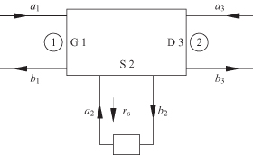
In this expression the subscript i represents s, g, or d, depending on whether the device connection is common source, gate, or drain terminated with Zs, Zg, or Zd . For example, rs = a2/b2 in Fig. E.1 or b2 = a2/rs . This is substituted in the appropriate place in the following equations. The incident and scattered waves from the three-port circuit are
(E.2)
![]()
(E.3)
![]()
(E.4)
![]()
When one of the ports is terminated with ri, then the circuit really is a two port. The scattering parameters for the common source, gate, and drain connection follow:
Common Source
(E.5)
![]()
(E.6)
![]()
(E.7)
![]()
(E.8)
![]()
Common Gate
(E.10)
![]()
(E.11)
![]()
Common Drain
(E.13)
![]()
(E.14)
![]()
(E.15)
![]()
(E.16)
![]()
A numerical example illustrates the process. A transistor with a set of common source S parameters at 2 GHz is given below:
![]()
![]()
![]()
![]()
These are then converted to two-port y parameters. These will be called y11, y31, y13, and y33. The indefinite admittance matrix is formed by adding a third row and column such that the sum of each row and the sum of each column is zero. The resulting 3 × 3 set of y parameters are obtained:
![]()
![]()
![]()
![]()
![]()
![]()
![]()
![]()
![]()
These are then converted to three-port S parameters using Eq. (10.32) as originally given in [1]:
![]()
![]()
![]()
![]()
![]()
![]()
![]()
![]()
![]()
At this point it is desired to transform these parameters to common gate parameters in which the gate is connected to ground through a short circuit. The resulting common gate two-port S parameters are found from Eqs. (E.9) through (E.12):
![]()
![]()
![]()
![]()
With the transistor now characterized in the orientation that it is to be used in the oscillator, a choice is made for the impedance at the generator side. If this impedance is chosen to be a 5-nH inductor at 2 GHz, the output reflection coefficient is
![]()
This shows that oscillation is possible under these loading conditions. The above expressions for the revised S parameters can be found in [2] using slightly different notation.
REFERENCES
1. K. Kurokawa, “Power Waves and the Scattering Matrix,” IEEE Trans. Microwave Theory Tech., 13, pp. 194–202, March 1965.
2. R. M. Dougherty, “Feedback Analysis and Design Techniques,” Microwave J., pp. 133–150, April 1985.